electronics production
Recall that as part of my final project, I am making an I/O board with button-bearing daughterboards that will handle the buttons on an MFD:
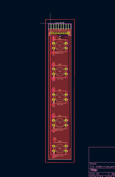
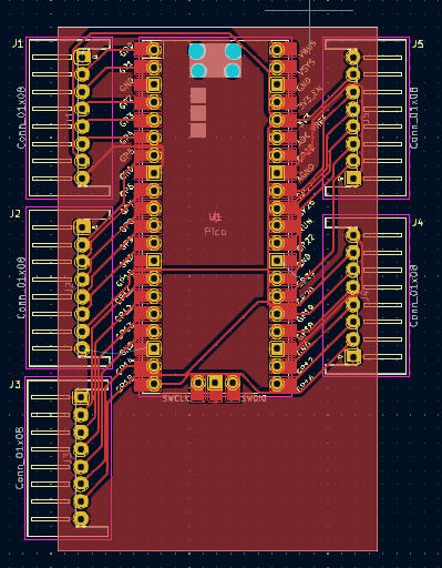
Daughterboard and I/O master board designed last week:
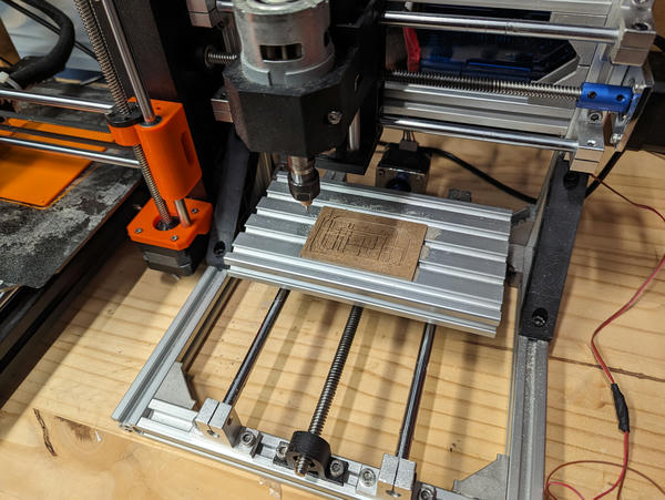
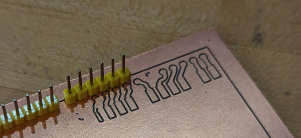
I milled the I/O master board this week in Reponsive Environments' PCB router:
partial redesign
I redesigned the boards this week because I realized last week's was needlessly complicated — I wasn't making use of the fact that the GPIOs have pullups, which meant I routed power to each daughterboard and needed to add resistors for current-limiting.
I removed that requirement, cutting out two wires per daughterboard connection (I had rounded up to 8 wires using two grounds, since I didn't want an odd number of pins in my connector). More importantly, the lack of power going to all connectors drastically simplified the single-layer routing topology problem and allowed me to use larger traces (much nicer for PCB milling).
I also added SMD debounce capacitors (22μF — just what I could find around ResEnv in quantity 25) to the I/O master, as I've never implemented debouncing in hardware before and wanted to try this. Unfortunately, these additional footprints along with my desire to keep the design compact caused me to decrease my trace width and spacing significantly. This would come back to bite me later.
debounce verification
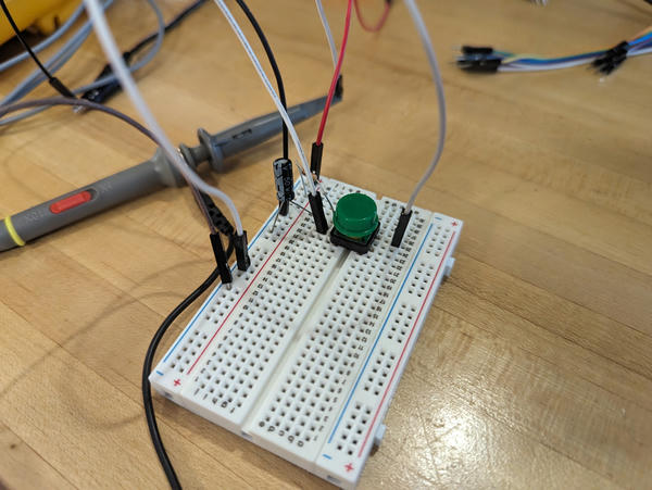
I built a prototype of the debounce circuit before I milled anything to verify behavior:
Here's a plot of a button actuation at the measurement point on my scope, full vertical range 0V - 3.3V, 10ms/div:
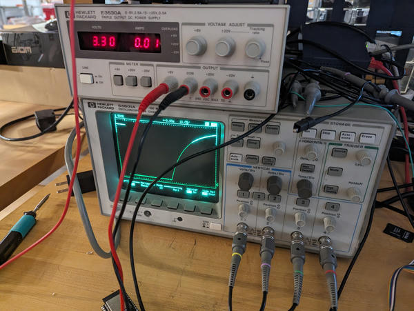
I tried a bunch and couldn't produce a button press that was noticeably noisy.
Then I built the same circuit using the SMD caps I had on some protoboard — back:
And front, with button:
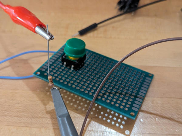
I saw similar performance with this protoboard version of the circuit, validating the design.
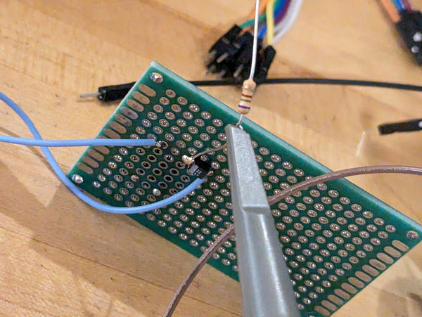
aside: tantalum caps
I believe the capacitors I found are tantalums. It's hard to know for sure, as they were in an unmarked reel-tape, but they do have a polarity marking. Tantalums have the opposite polarity-marking convention as electrolytics, so this makes deciding which way to orient them a dilemma.
Prima facie, that they are in an SMT package suggests that the caps are tantalums, as to my knowledge elecrolytic caps are not packaged for SMT this way. However, I could be wrong, so I wanted to do some investiagion.
I used a multimeter to check the capacitance in both directions, hoping something about their polarization would cause the reading to be obviously different one way. This wasn't the case — I got 22μF both ways.
I installed them in my test circuit under the assumption they were tantalums, and nothing blew up, so that lends some credence. They're marked 5V as well, and my circuit is at 3.3V, so it's not like they're way under their rating.
On the other hand the resistor in this test circuit limits current to 2mA maximum (at 3.3V), so let's generously say the capacitor could convert 10mW to heat under the worst conditions. This seems unlikely to generate enough temperature differential to cause a catastrophic failure, supposing the caps are of a different type.
So, altogether hard to say, though it seems circumstantially likely that they are tantalums.
milling
I used FlatCAM as my CAM tool this week and Candle as my machine controller (communicating to the router over USB serial).
I had a lot of trouble getting my boards to mill properly. Initially, I wasn't getting enough depth of cut — the first run didn't make it through the copper. A later run was well-enough calibrated (but still wrong) that it only burnished the top surface of the copper without cutting.
I had difficulty debugging these problems because FlatCAM and Candle are both new to me, so attribution of the behavior was difficult. I'd think I had solved one problem, but it would surface another one, and I couldn't tell e.g. if I wasn't cutting deep enough because I was zeroing the machine incorrectly (or upsetting the zero, etc.) or because FlatCAM wasn't setting a deep enough cut depth in the first place.
Eventually I understood what each tool wanted and got everything working, including Candle's heightmap feature:
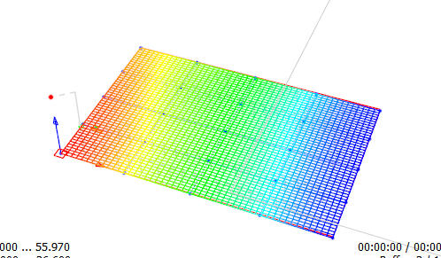
Red areas are high, blue are low — for our PCB mill, the bed slopes down to the right, so the zero is correct on the left, but drastically off on the right.
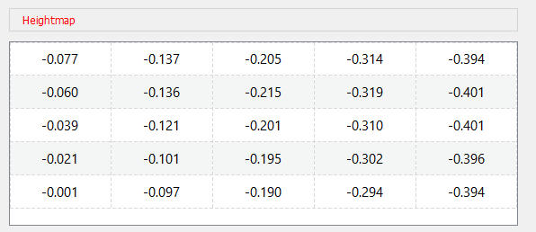
This is the table of each probe point (in mm). Our depth of cut is only 0.15mm, so we would expect to stop cutting entirely halfway across the bed. In practice, this doesn't actually happen, which (along with a tendency to mill overly-wide paths with our v-bits) leads me to believe our zero process has some bias. In any case, there is a lot of drop-off wrt. our depth-of-cut across the bed, so this mesh bed-leveling process should be helpful.
Once I got to this point, I quickly realized my design wasn't going to work. The trace width and trace spacing reduction (both 0.25mm) I had made to accommodate the debounce caps made the traces too narrow for our mill — they were either very stringy (tending to get grabbed by the mill and ripped off) or missing entirely.
reredesign
I redesigned again, this time omitting the debounce caps entirely and just resolving to handle this in firmware. The I/O master board is very simple now:
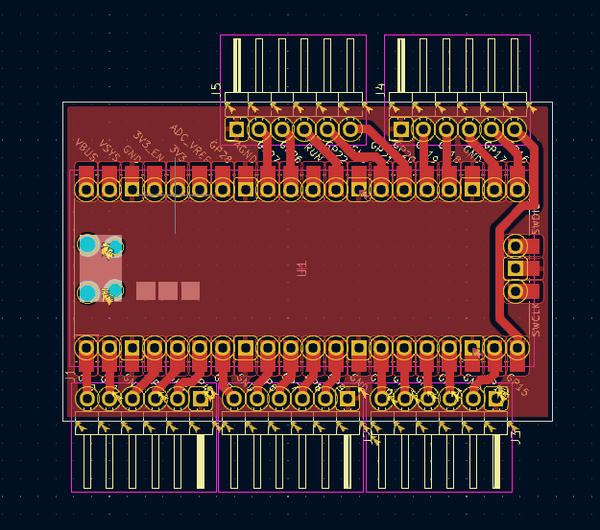
It just forwards ground and 5 button IOs to a pin header connector. This is at the very least nicer for my application than directly plugging the button IOs into the Pico as we can share ground in groups of 5 IOs rather than 4.
NB: there is 1 extra button group of 5 IOs for auxiliary functions on the MFD (day/night, brightness encoder, contrast).
I increased the trace width to a full 1mm and minimum clearance to 0.5mm to ensure we would mill cleanly.
milling, part 2
shifting
The last hurdle to clear was the board shifting during milling. I had seen this several times, and am still not sure why, beyond potentially inconsistent application of double-stick tape. I even tried my first attempt with halved feedrate in an attempt to minimize tool force on the part, but it still shifted:
(This is on the back of my successful board — ignore the pins.)
The pads are all meant to be the same size as the six on the right, but you can see that the last four get successively smaller as the double-stick tape started to release and the board really started to move, at which point I killed the job.
success
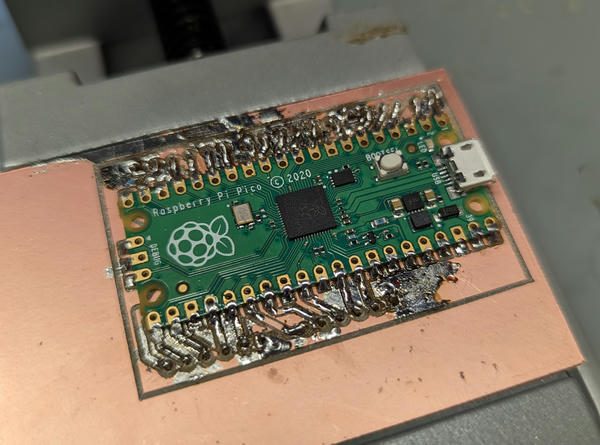
The next attempt worked. I didn't change anything beyond making sure I held firm pressure on the board for 30-45 seconds to ensure it had the best bond with the tape possible.
drilling
Operationally, drilling proceeded smoothly. I could keep the same zero and heightmap and just start it. I was conservative and started at 33% feedrate, and slowly ramped to ensure nothing would break. It completed without shifting or any other issues from the machine.
drill depth
However, functionally, I did hit problems. First, I hadn't set the drilling depth deep enough (1.7mm, should have used 2mm), so the drill failed to pierce the copper on the back side of my FR1. I hadn't noticed this until I had pulled the part off of the mill, or I would have just re-drilled it. Instead, I finished the drilling manually with the same bit in a Dremel — the existing holes made this easy.
The downside to doing this was that I didn't have a backer board, so I had little copper tags attached to most of the holes. This was an issue because they would almost certainly contact the header pins and short all of them to each other. I removed them by hand using a drill bit as a deburring and slight countersink tool.
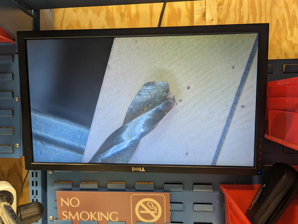
This had the added benefit of relieving the copper at the edges of the holes, making incidental contact between pins and the bottom plane of the board almost impossible.
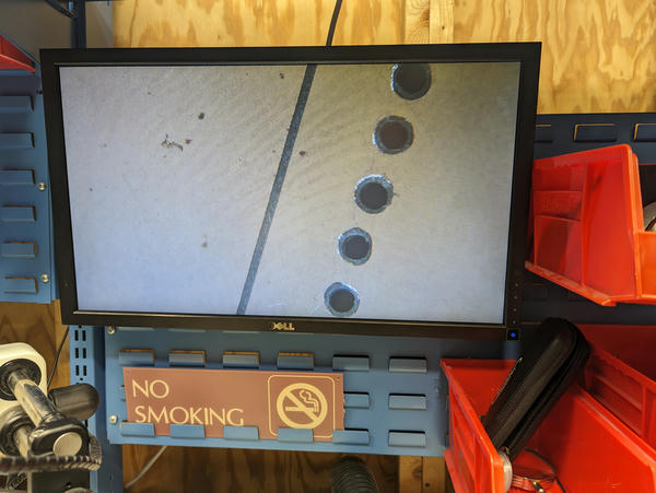
oversize holes
The second problem was larger: the holes were oversize. Nominally, they should have been 1mm, but the endmill I had measured 1.06mm. I didn't think this would be too much of an issue, as the thinnest annular width I had for any pads was 0.35mm — the oversized endmill should have only affected this by 0.03mm per side, i.e. < 10%.
Unfortunately, I actually totally lost most of my small pads. If you recall, I wasn't able to mill traces at 0.25mm, so 0.03mm was 33% of the way from our 0.35mm to a known non-working configuration — suddenly much more significant. That's not to say that a 1mm endmill would necessarily have done the trick, but it's likely we're playing with the border of process stability, so that small change was much more significant than I expected.
soldering
better known as: i sure wish i had some solder mask
The result of this drilling mishap is that I spent several hours soldering and continuity-testing the board. Perhaps a better term than soldering would be "solder sculpting" — to get the solder to bridge only to the header pin I wanted across a void where a pad should be and without solder mask (mostly: without bridging to my ground pour), I had to develop some techniques.
It is first worth noting that I had all my trouble connecting the header pins, which are the connectors for the daughterboards, and are through-hole. The castellated edge on the Pico was very straightforward and took me all of two minutes.
techniques
-
General principles:
- Solder "likes" heat — it tends to move towards the hot thing
- Effective heat conduction increases nearly as a stepfunction when solder melts — as a liquid, solder drastically increases its surface area with the iron and other solder, meaning the iron is more heat-efficient and more solder is exposed. This is a cascading effect.
- Electrical nets are correlated to thermal nets
- A hot board / still-hot solder melts much more rapidly
- In general, for "atypical" soldering techniques I'm discussing here: if you don't get the result you want, don't keep trying — remove the iron immediately, wait for the board to cool, and try again. It only gets more difficult to be precise the hotter the board is.
-
"Flicking" solder: build up an oversized blob of solder on a trace, then lift it with the point of the soldering iron. The bottom of the blob stays stuck to the trace, and gravity keeps most of the mass there. You end up with a tail of solder that you can lay on top of the pin you want to solder to and remove the iron so as to elongate the tail. The joint with the pin (if any) will be cold, so you will need to touch it up. It can help to build a blob, wait and let it cool (not just to where it solidifies, but for 10 or 20 seconds so it loses residual heat), and only then flick it — hotter solder is runnier, and we want it to be viscous here.
-
"Tapping": in most cases, the cascading increase in heat conduction due to solder melting is helpful. However, if we want to touch up a joint, this effect can lead to everything becoming one big contiguous puddle of solder very quickly. With a well-timed application of the iron you can sometimes manage to affect only part of a joint, or to quickly bridge two parts together without wrecking the rest of the solder structure. Suppose we've "flicked" a tail near a pin (but not touching). We can connect the tail and the pin by flicking a tail from the pin and tapping to weld them together. This works best if there is a natural heat brake — a piece of (non-solder) metal in the conduction pathway can stall other parts of the solder body from melting and give you some time to work locally.
-
Preheating: for both flicking and tapping, if you can selectively preheat the part you won't be acting on, it makes it much easier to produce a solid joint — it will tend to attract solder.
-
"Towering": it's possible to build a solder tower by tapping successive blobs on top of each other. This is useful if you can establish a known-non-shorted base blob on a trace and then tower up (usually once) to flick to a pin, because it means you need much less of a large blob.
-
"Pin blobbing": I discovered over time that this was the most consistent approach for most pins. Rather than trying to flick from a trace, build up a blob on a pin, ideally let it cool somewhat, and flick to the trace. Traces are usually packed more closely to other traces and the ground plane than pins, which have breathing room for the pad, so building a blob on the pin is preferable. Flicking quickly and at the right timing after placing the blob makes this work — a blob with some heat will tend to pull solder towards it, and if you make the flick fast (i.e. cold), you will minimize risk of bridging to an unintended net. Again, a preheated target trace will tend to improve the chances of a nice joint without needing to touch up.
ground connections
The ground connections were the absolute worst to solder. They have thermal relief intentionally and a copper pathway for solder to spill to the ground plane, so it's impossible to keep a solder blob within the pad. I needed to tower for these, for the most part. They also need to be done first, because the quantity of solder you need to make these connections means that they will frequently bridge to other already-complete pin connections and melt them into a big blob.
connectivity
I verified my joints with a multimeter and microscope. To my knowledge, everything is electrically connected properly, except one GPIO that is shorted to ground. I believe that issue must be underneath the Pico, as I've scoured all along the visible parts of it and can't find anything wrong.
I specifically checked every connection against bridging to ground and the board's nominally floating reverse plane. I didn't do a pairwise pin-pin check for shorts, and I haven't checked against power, either. Each assigned GPIO on the Pico does have continuity to its corresponding pin on the headers.
There is only one GPIO that is shorted to the reverse side's copper plane, so other than being a big antenna, it should work properly. The reverse plane is not shorted to ground.
Unfortunately, there are 6 test points on the reverse of the Pico that I didn't account for in my design — I anticipate they are shorted together and to ground. I haven't checked the schematic for what they connect to, but I would expect that it breaks the board.
programming
NB: To the extent this matters for the grade, I did successfully program a nearly-equivalent board for my final project with almost exactly this firmware.
Unsurprisingly, given that I think the board wouldn't power on, I didn't program the board for this week. It's very basic firmware for what I need — could just be a polling loop:
// This firmware prototype intended for use with Arduino framework.

#include <Joystick.h>

Joystick_ joystick();

constexpr uint8_t N_BUTTON = 25;

const static uint8_t PIN_MAP[N_BUTTON] = {
    // elided
};

void setup() {
    for (auto pin : PIN_MAP) pinMode(pin, INPUT_PULLUP);

    joystick.begin();
}

void loop() {
    for (auto i = 0; i < N_BUTTON; i++) {
        auto pin = PIN_MAP[i];
        auto state = digitalRead(pin);

        joystick.setButton(i, state);
    }
}
Ideally I'd make it work with interrupts, but this would be fine.
As I said, I would have tested this, but I'm pretty sure the board I have would die if I plugged it into power, and I'm out of time for this week to debug it or produce another.
improvements
The easiest and most significant improvement I think would have been not using through hole parts. I thought this would be interesting, but it really didn't work. Surface-mount connectors and I could have been done with the soldering in less than 15 minutes, and I wouldn't have needed to drill at all (not that this took that long).
The better project this week would have been the daughterboards, as these are simple and lend themselves much more readily to exploring milling a board, but they're larger than the capacity of resenv's PCB mill, so I would have needed to use the CBA one. Unfortunately, there were multiple people lined up to use it every time I stopped by, so I couldn't do it this week.