How to Make (almost) Anything 2023 | Week 6.1: Electronics Production
Home
Assignment: Group Project -- Characterize the design rules for your in-house PCB production process send a PCB out to a board house; Individual Project -- Make and test the development board that you designed to interact and communicate with an embedded microcontroller.
Individual assignment: Make and test the development board
Description: Utilizing the KiCad PCB design from week 5.1, I converted the output from KiCad into G-Code via the Mods platform. This G-Code file was then fed into the software communicating with the CNC PCB mill to produce the physical PCB.
Primary files:
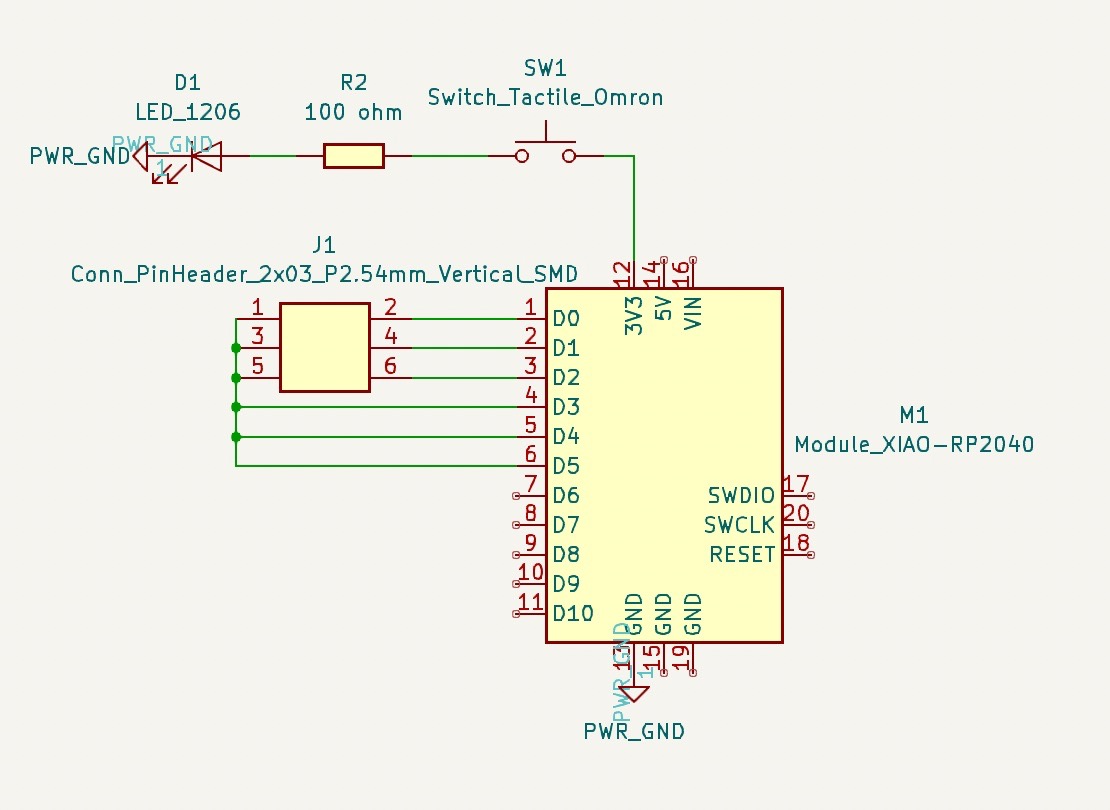
- Electronics Design PCB schematic and design (KiCad)
Procedure:
- Taking the PCB design from week 5.1, export the design as an SVG file
- Convert the F.Cu and EdgeCuts SVG files into PNG files using Adobe Illustrator, then edit the EdgeCut PNG by adding a white rectangle over the inside of the edge cut design
- Using the Mods platform, right click and select "programs" > "open program" > "mill 2D PCB"
- Upload the F.Cu PNG file to the Mods platform, and select "mill trace (1/64)" under "set PCB defaults" and select "calculate" under "mill raster 2D"
- Validate the G-Code path appears as expected, and export the G-Code output
- Upload the EdgeCuts PNG file to the Mods platform, and select "mill outline (1/32)" under "set PCB defaults" and validate the desired tabs under "image tabs" prior to selecting "calculate" under "mill raster 2D" (note: I experienced a bug on the Mods platform where the tabs were not properly attached to the edge cut outline, but Mods would crash when only one tab was selected; given this, both tabs were kept although only one tab provides structural support to the edge cut)
- Validate the G-Code path appears as expected, and export the G-Code output
- Import the F.Cu G-Code file to the desktop attached to the CNC milling machine
- Prepare the CNC by clamping down a sacrificial sheet of copper (bottom) and the milling sheet of copper (top), then secure the 1/64 end mill using the blue guide to determine proper end mill depth
- Move bit to x=0, y=0 and then ensure the ground lead is attached to the top of the probe before zeroing the z plane
- After the z dimension has been probed and raised, remove the ground lead from the probe and insert the plasstic cover over the end mill then turn on the vacuum
- Press play on your mill trace
- Upon completion of the mill trace, turn off vacuum, remove plastic cover, and exchange the end mill for the 1/32
- Upload the EdgeCuts G-Code file to the desktop attached to the CNC milling machine
- Repeat steps 10-12 with the 1/32 end mill for the mill outline
- Upon completion of the mill outline, turn off vacuum, remove plastic cover, and snap PCB from the copper sheet
- Inspect the PCB to ensure the trace was clean and as expected; If complications occurred, adjust design as needed and repeat PCB production
- Solder the specified components onto the PCB
- Inspect the soldered component to ensure there are no shorts within the circuit
- Validate the circuit by powering the Xiao RP2040 and ensure the LED turns on as anticipated
Key learnings:
- Inspecting your PCB throughout the process can save time debugging at the end -- It can be very helpful to undergo inspection / sense checks with your PCB at each major checkpoint throughout the design and production process in the hopes of catching an errors early on before it is produces and covered by components / solder that may hide small errors within the PCB
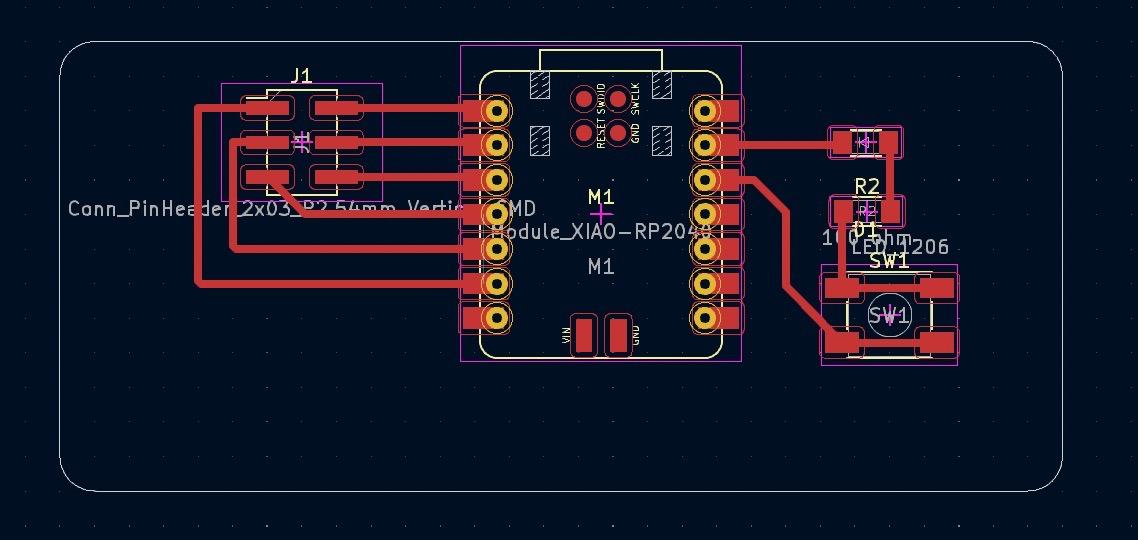
KiCad developement board design (Week 5.1)
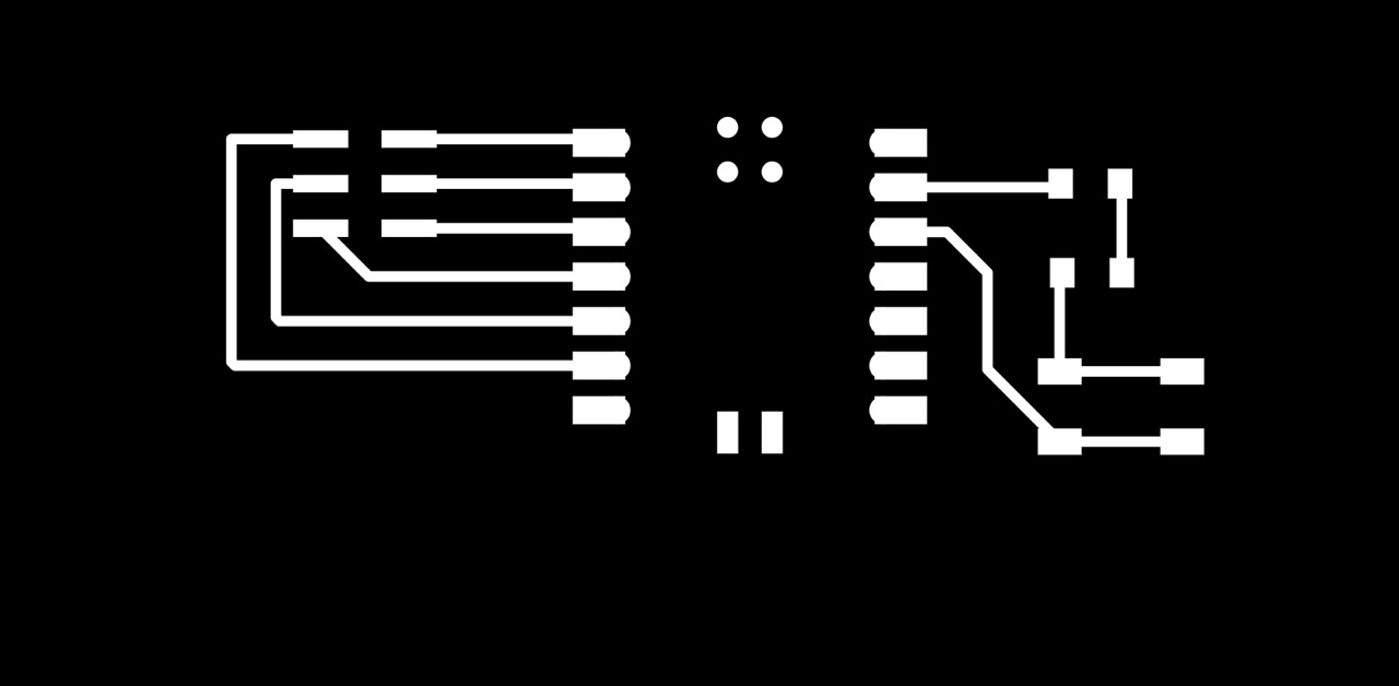
PCB trace footprint
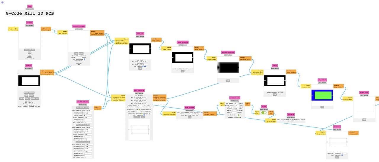
Mods conversion of PCB PNG to G-Code
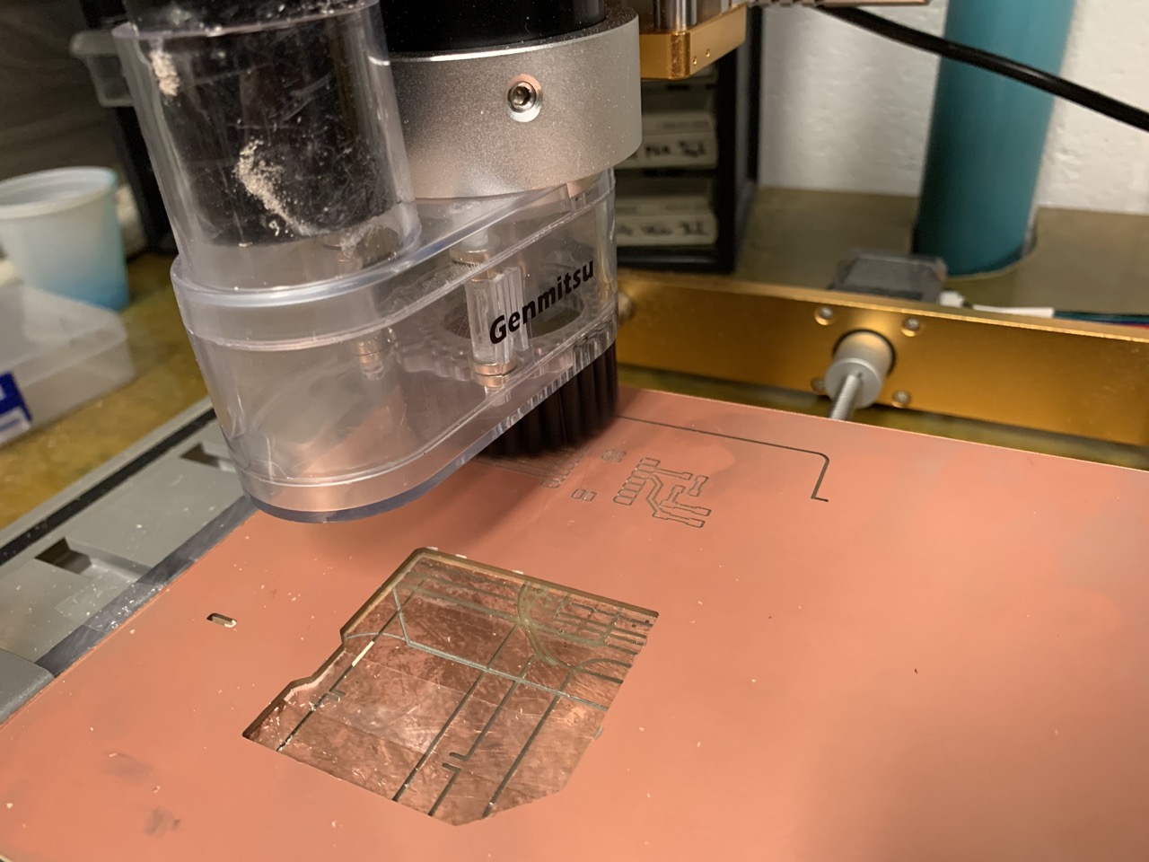
CNC PCB milling in progress
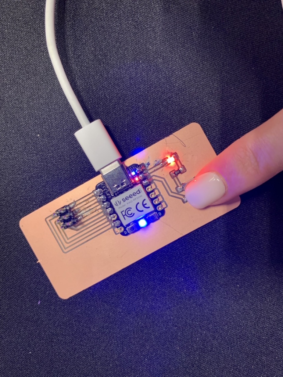
PCB production output: LED lights up when button is pressed