HTMA Week 10: Output Devices
Published: 2023-11-08Preface
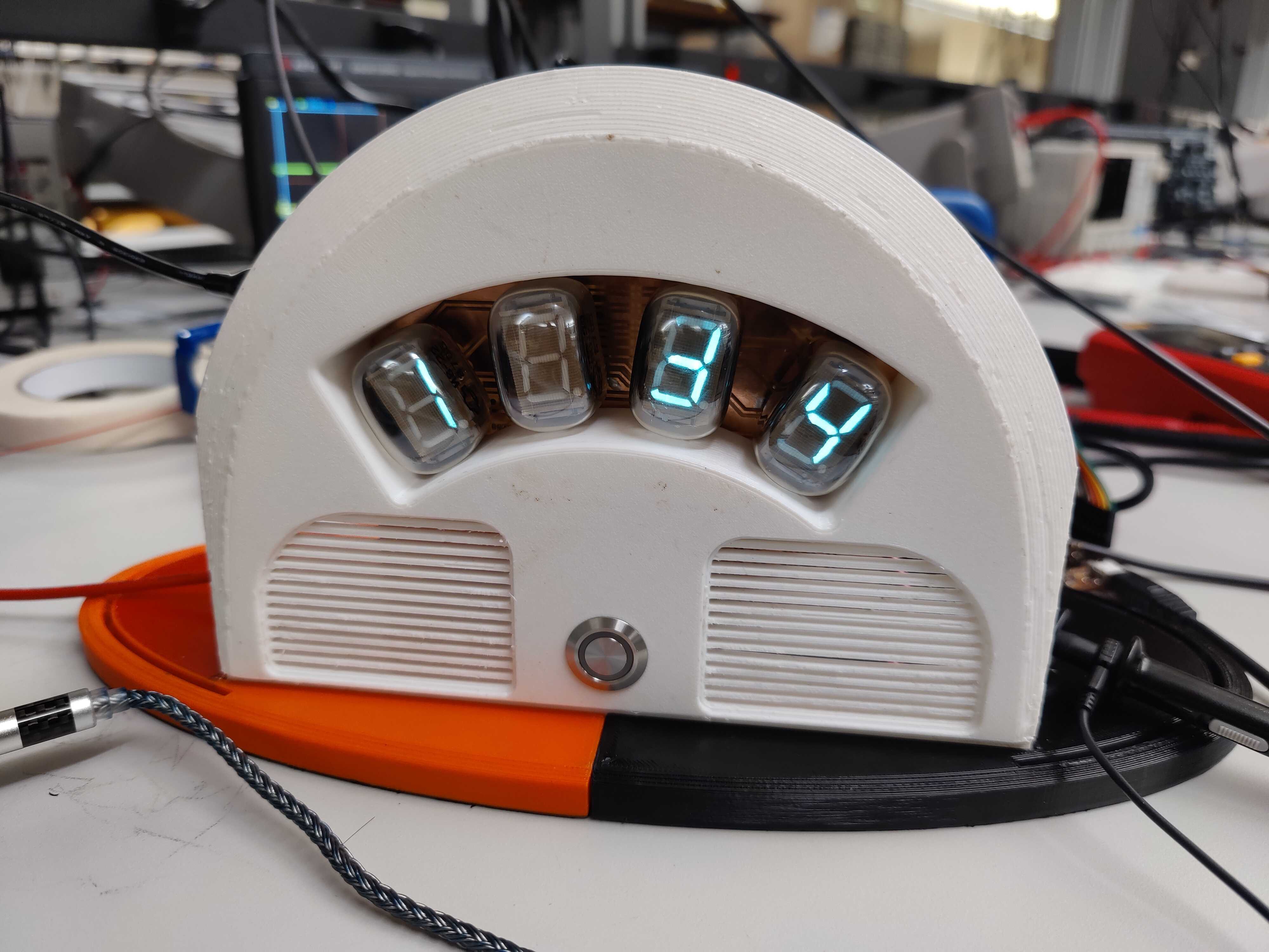
So for this assignment, I decided to expand on my week 5 project of making a VFD display and improve on its design, while making the display board for my final project. The two major changes are that there are now 4 multiplexed VFD displays, and now we use highside switches on the anode as well as the grid pins of the tubes.
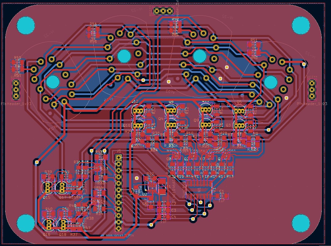
Schematics

Bit small to read, should right click and open it
Multiplexing
This board will be connected to the final project’s main board, which will make use of a ESP32-S3. The microcontroller will interface with the 74HC595 shift register in order to control what segments are lit through the 8 high-side switches. While the outputs of the segment high-side switches are connected to all 4 VFD tubes, the microcontroller also has control over which VFD tube to turn on with the VFD#_EN pins, which control 4 additional high-side switches for the grid pins of each VFD tube. Multiplexing like this dramatically reduces the amount of pins and shift registers we need to drive multiple displays, and saves on a bit power consumption (couple mA) since only one tube should be lit at a time.
High-Side Switching
The week 5 schematics pull-up resistors to 27V at the anode pins, while the shift register outputs control which segment to turn off. In contrast, the new design uses high-side switches for the anode pins (and grid pins) in order to prevent 27V from being connected to every anode pin at all times and constantly drawing power. However, this does come at the cost of extra resistors and transistors per pin.
Manufacturing
To get the smallest features milled, I needed end-mills smaller than 1/64. Luckily, Anthony had acquired 8/1000 end-mills for his “Make Your Own Xiao” wildcard week, so I was able to use that to mill my small features… or so I thought. The tool broke 5 seconds into the mill, so I ended up using the engraving bits instead to create my small features. The total process took about 4 hours, then another couple of hours to solder everything in place.
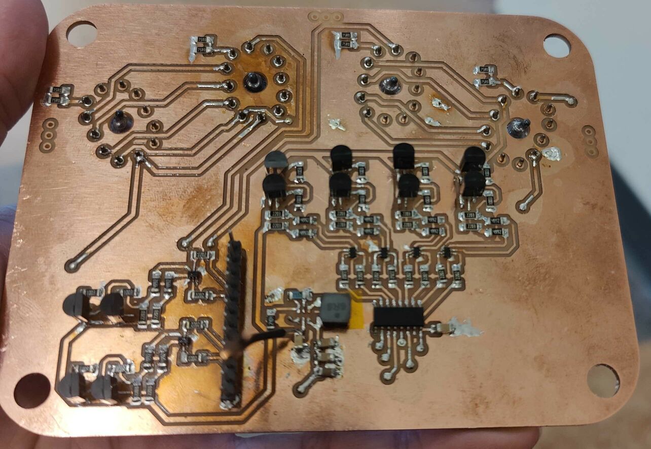
Front of the PCB
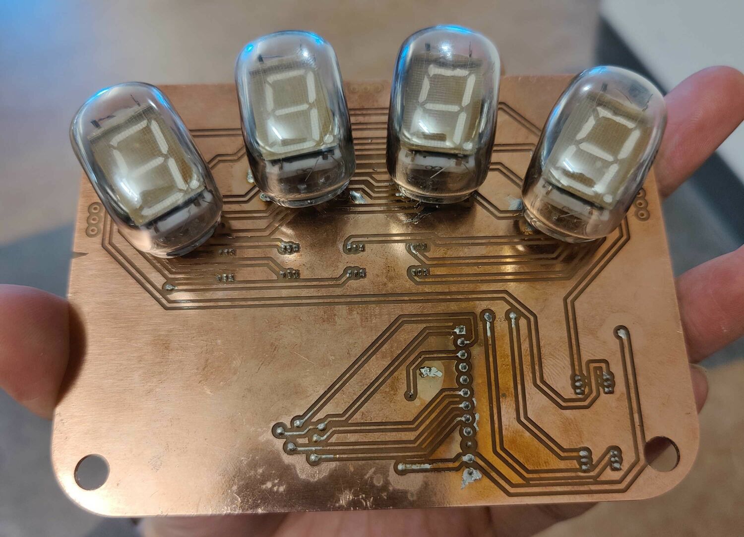
The VFD tubes go on the back
Software
To test things out, I first hooked it up to my main board and tried some simple code. I set all 4 grid control pins as PWM outputs, and configured them such that they each occupy a quarter of the available duty cycle, so that at most only one pin is on at a time and they’re cycled through at the frequency of the PWM signal.
One interested thing I figured out that you can do is that you can interact with shift registers as if they’re SPI devices. All you need to do differently is to connect your Chip Select (CS) pin to the register clock of the target IC, and configure your SPI bus to pull CS low when writing and back to high at the end.
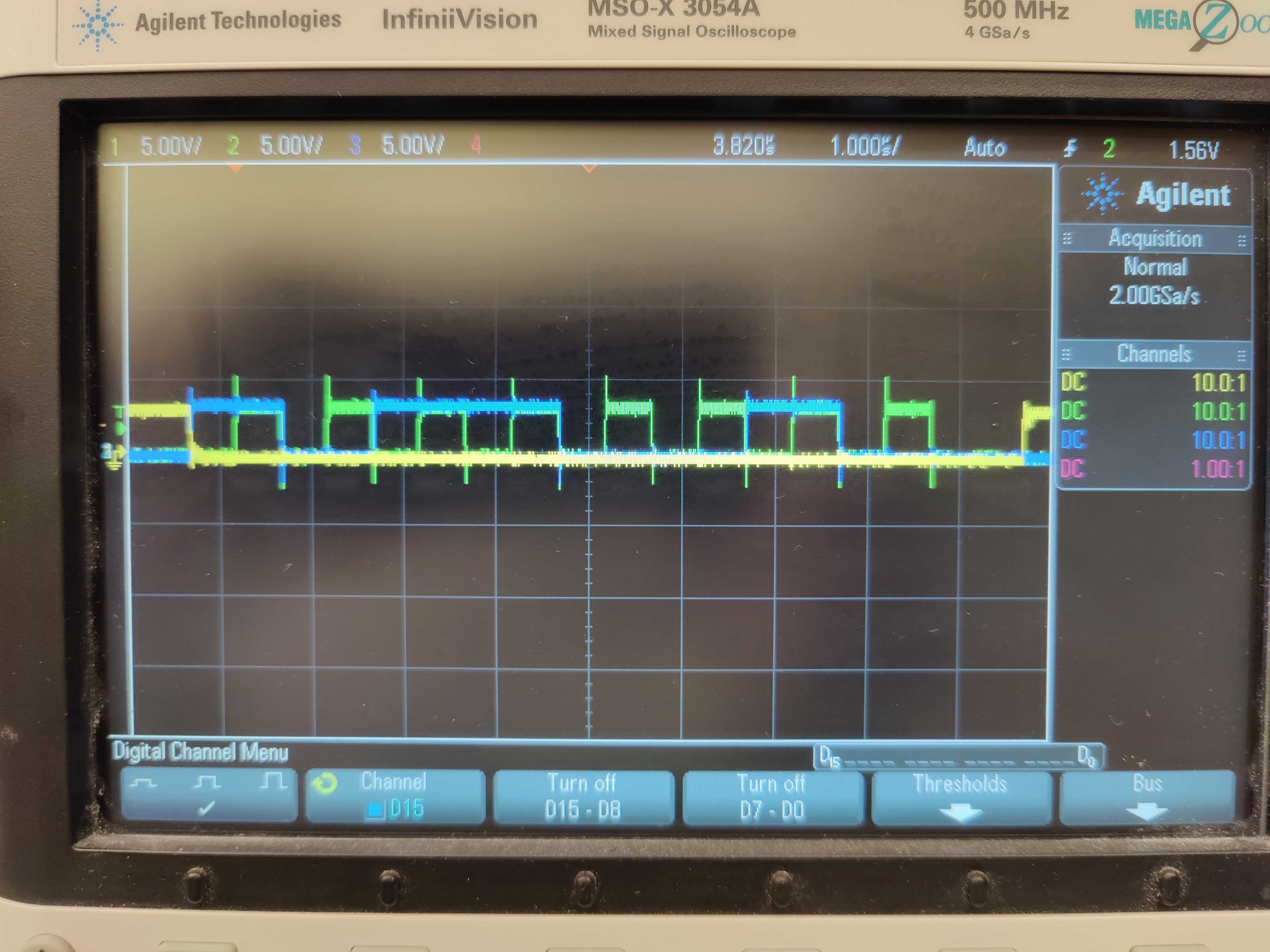
Green: Clock, Yellow: CS, Blue: Data
With SPI and PWM set up, I tried to turn one segments only one at a time, and got what I expected.
To have different digits display different numbers, we then need to scan through each grid pin, enable it while disabling the others, then writing what segment we want to be lit over SPI.
To achieve this, we unfortunately have to abandon PWM, since it does not support callbacks between duties. I instead followed ESP32 documentation to to set up a hardware timer to periodically invoke a function that updates the spi transmit buffer changes which tube is on. To reduce function calls and update each VFD’s grid pins collectively, I set up a dedicated gpio bundle on them so I can change them all with one call to dedic_gpio_bundle_write. Finally, we can display different digits on each tube.
static bool change_digit(gptimer_handle_t timer, const gptimer_alarm_event_data_t *edata, void *user_ctx)
{
    digit_index = (digit_index + 1) % 4;
    vfd_transaction.tx_buffer = vfd_digits + digits_to_display[digit_index];
    dedic_gpio_bundle_write(bundleA, 0b1111, 0b0001 << digit_index);
    spi_device_queue_trans(spi_handle, &vfd_transaction, 0);
    return true;
}
Second tube was having issues when this was taken