Week 5 Assignment: Use an EDA tool to Design a Development Board to Interact and Communicate with an Embedded Microcontroller
For this week's assignment, I knew I wanted to design something that would eventually contribute to my final project. Having never even touched the tip of the iceberg when it came to PCB design, I wanted to design a board that mimicked the logic of my final project - essentially what I did during embedded programming week, but taken a little bit further
Naturally, I got sick during the week I knew nothing about and missed much of the long weekend (and the following HTMAA lecture - more on that on the Week 6 page). Between feeling too sick to work and playing catch-up in all of my classes, my timeline for the week assignment was pretty delayed, but I still got to a place I'm pretty happy with, given that this is completely new territory to me.
The first step was to decide what program to use. KiCAD had been recommended to me by multiple people when I mentioned this week's assignment, and I tend to dislike Fusion, so my choice of which program to start out with was pretty intuitive. Next all I had to do was learn to make a PCB in a couple of days - simple, right?
(Spoiler: I do soon realize that I should just watch the EDA recitation video, but I think it's worth documenting my failures even if they're just moments of stupidity)
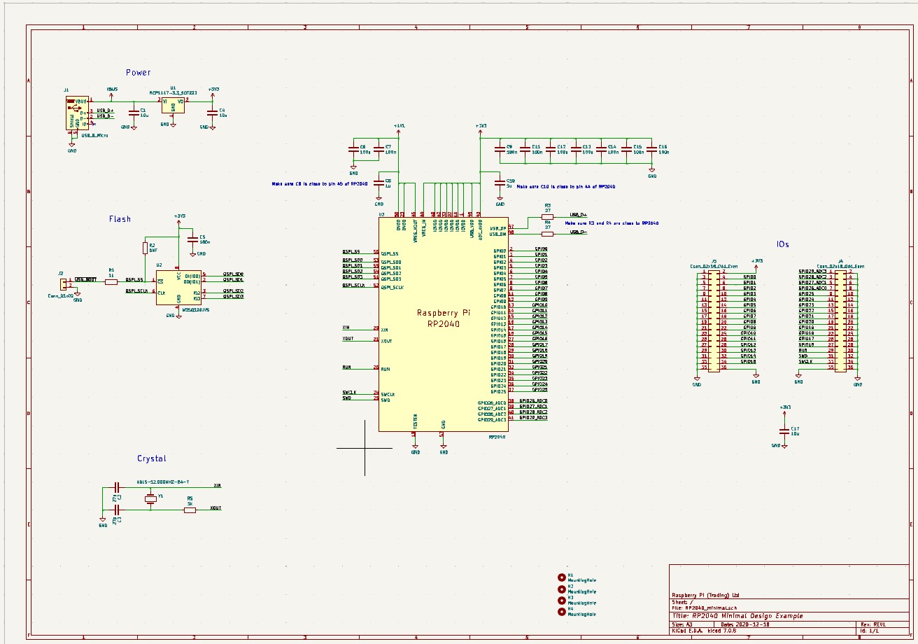
I found some documentation on the RP2040 and how to use it to design a PCB, and there was an example KiCAD file linked (the complicated-looking file shown in the image above). "This would be a great place to start, and I can just build off of this/add my components to the existing design" I thought to myself. Such was not the case. When I opened the file, it was nothing like I had expected, and I thought the barrier to entry to PCB design was much higher than it actually is. I spent some time fiddling around with various things inside the schematic editor and reading documentation, but never got far enough to document anything as I found myself quite lost.
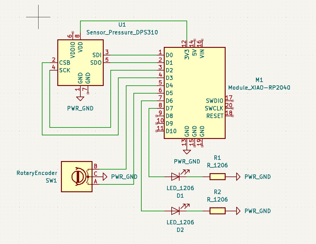
I ended up watching the EDA HTMAA recitation after about an hour of head-scratching. The workflow, which is obvious to me in hindsight, was vastly different than what I thought it'd be based on what I had read, and I was given a lovely starting point. For my design, I knew I needed to sense mechanical pressure and angular velocity, so I began by putting a pressure sensor (duh) and a rotary encoder into the design. I also wanted two LEDs as outputs, so I put those and accompanying 150-ohm resistors into the schematic as well.
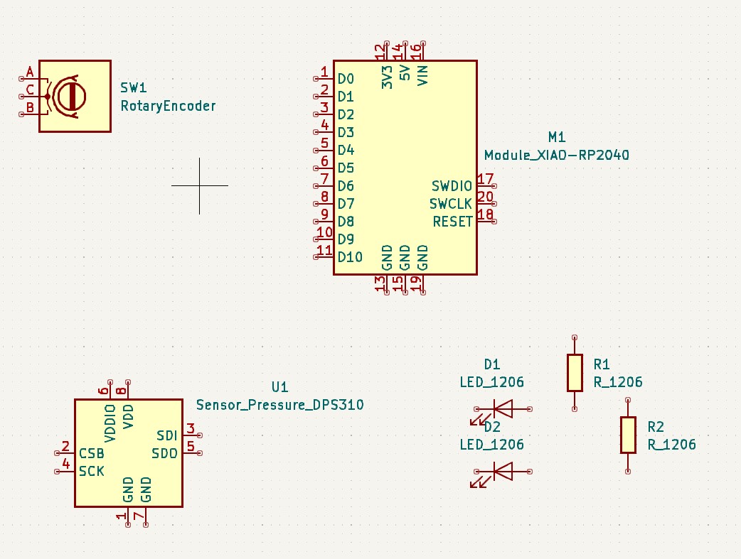
A few minutes later I had a pretty-looking schematic that was all wired up. Some wiring considerations: the pressure sensor from the Fab library is capable of software SPI communication, so I can wire some of its pins to any digital output on the Xiao. Also, I don't have any connectors/this isn't really a "development board"; this was partially due to initial misunderstanding on my part, but given that I didn't have many open ports and after talking to Anthony, I was ok with committing to this design to gain experience with PCBs and then going back in to make a dev board at a later time.
From here, I decided to hop into the board editor. My initial routing logic was "anything that worked" and the board ended up looking like this at first:
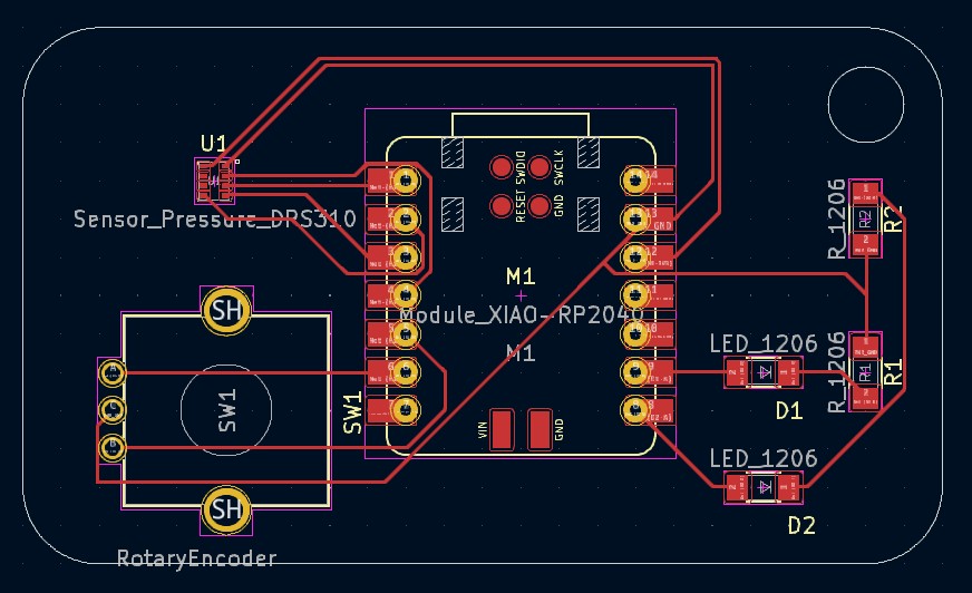
There are numerous problems with this first-pass design. First of all, I realized the rotary encoder I used wasn't from the Fab library, so I swapped it out for a potentiometer as a temporary way to approximate a linear encoder (this caused a small domino effect; only the first 4 pins of the Xiao are analog, so I had to swap out one of the SPI pins on the pressure sensor). Also, I had forgotten to set up my design constraints, which is crucial. A minimum clearance and track width of 0.4mm would ensure that none of the wires would be too close on the final board. I also moved my microcontroller up so that the USB-C port was hanging over the edge of the board a little bit. Finally, there were just several routing choices which could've been made easier, but I lack the experience to quickly diagnose the "right" routing solution. Thankfully, Anthony was a big help in getting me to think about routing in a better way. After all of these changes, my final design looked like this:
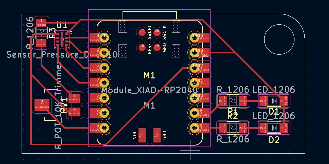
This is significantly more space-efficient, looks cleaner in general, and it uses a jumper resistor to bypass a minor routing problem.