Week 6 Assignment: Make and Test the Development Board that you Designed to Interact and Communicate with an Embedded Microcontroller
This week, I set out to mill and solder the PCB I designed last week. After some R&R from my illness last week, I was in a better starting spot for this assignment.
My first step was to plot the KiCAD PCB design into Gerber design files. This step is quite simple, as it turns out; my PCB is single-sided without too many complicated parts, so adter selecting "file - plot" in KiCAD, deselecting all options except for the front side copper (F_Cu) and edge cuts (Edge_Cuts) in the menu on the left of the window, and ensuring "Generate Gerber job file" was selected, I just clicked "Plot" and I had a folder with my files ready to go!
Before moving on to the PCB mill, I went to jlcpcb.com to generate an image of my milled PCB based on my Gerber files to make sure I had plotted correctly. Once I had verified that, I uploaded my Gerber files to the lab computer attached to the PCB mill:
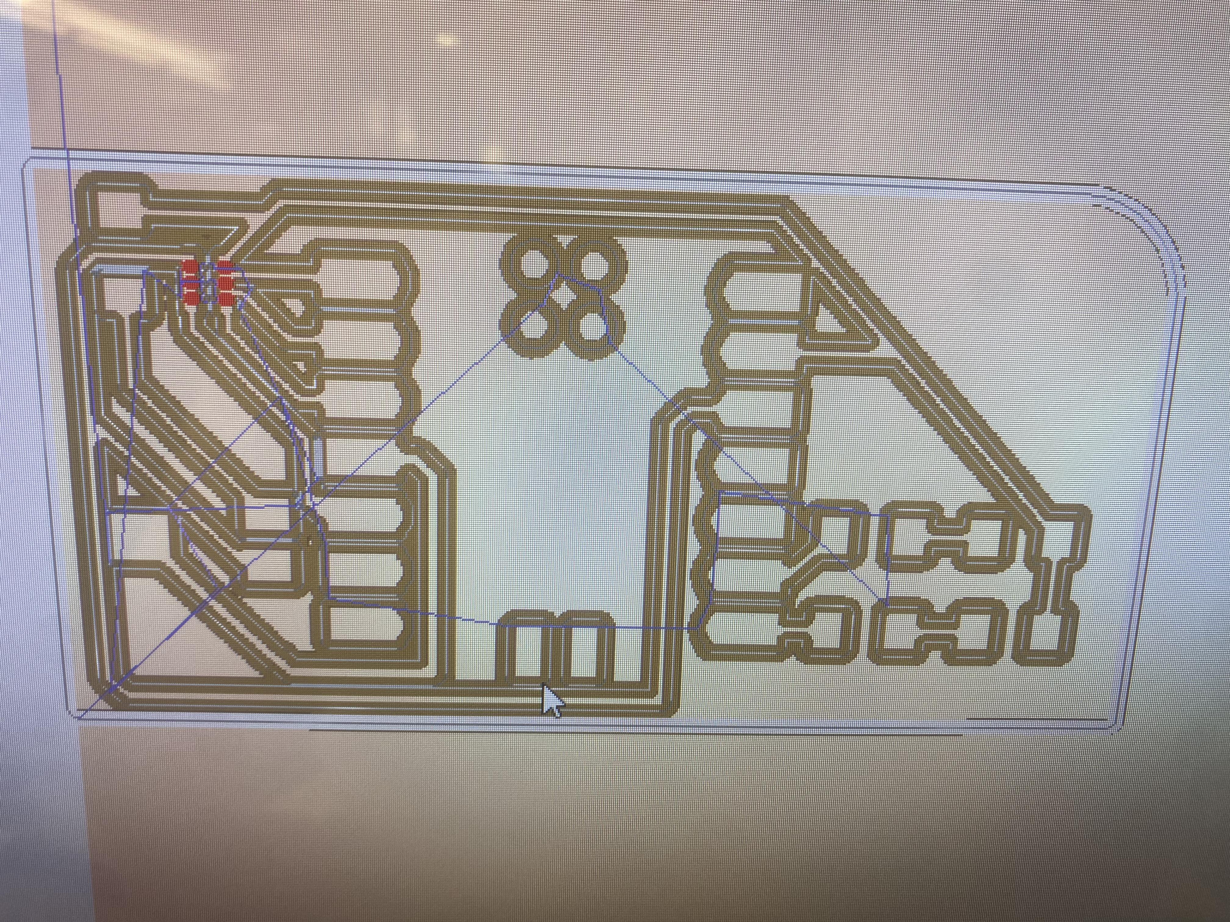
This looked right! The parts highlighted in red would need to be milled with a 1/64" endmill instead of a 1/32" endmill, but some minor changes to the print settings (with Anthony's help) allowed me to set that up easily. I just had to make sure it milled with the 1/64" first, and then did the remainder of the copper cuts plus the edge cuts with the 1/32". Though I had never milled a PCB before this week, I came in quite comfortable with CNC manufacturing in general, so I knew the care to take, especially with these tiny and fragile endmills. My job was about a half hour long, and after it was done, I had this:
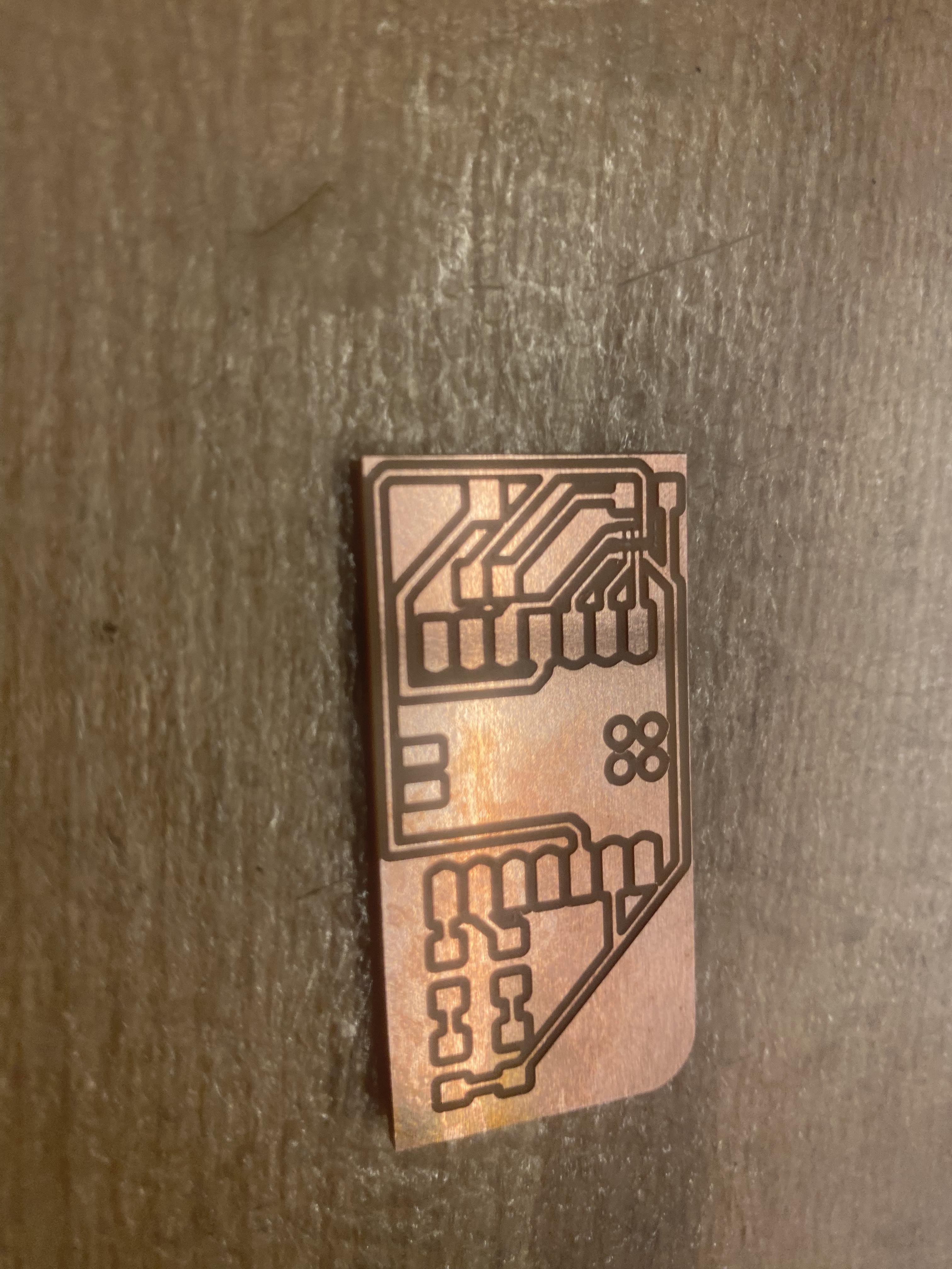
There was a small burr around the edge of some of the cuts, but this was easily resolved with some light sanding. The next order of business was to solder my components to the board. Here, I ran into a couple of issues. Firstly, the pressure sensor I wanted had not arrived in the EDS' stock yet. Secondly, it was an atmospheric pressure sensor, not a mechanical pressure sensor. After some internal chuckling at just how out of it I had been the week before, I decided to move forward with whatever I could on my board as it was already Tuesday night and I had many more weeks to create and test better PCBs (note from the future: in Week 9, I essentially completed this week's assignment in a more satisfactory manner in addition to the input devices assignment).
Anyway, I had to learn to solder things onto a PCB. I came in very comfortable with soldering, but multiple of my PCB components (particularly the LEDs and resistors) were a little bit too small for comfort. It was at this point that Alec introduced me to the wonders of solder paste. With this, I could place a tiny dot of the paste onto the contact points I wanted to fasten a component to, almost like glue. Then, I carefully pressed my component into place in the paste with tweezers, subsequently using a hot air gun to heat up the solder and fasten the component to the board. I loved doing this and ended up with this result:
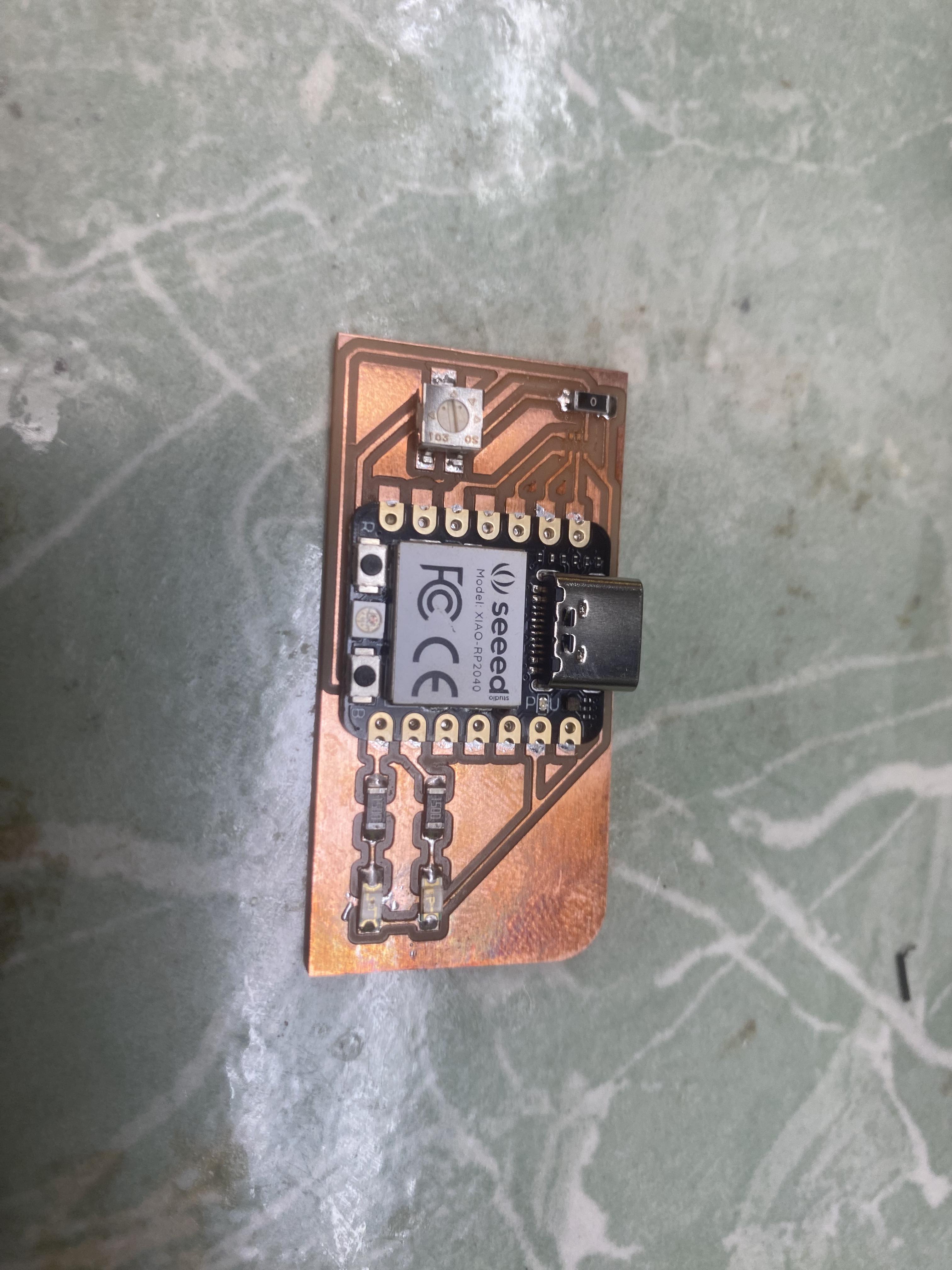
It wasn't all that much, but it was something. I was ready to devote my time to making up the remaining work from this week's assignment in a subsequent week.