Week5
tldr: doggie board!
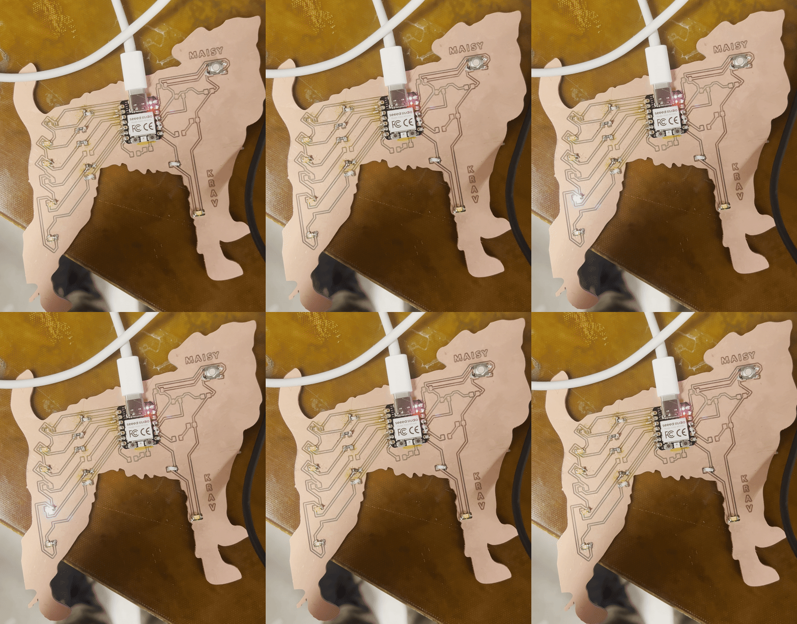
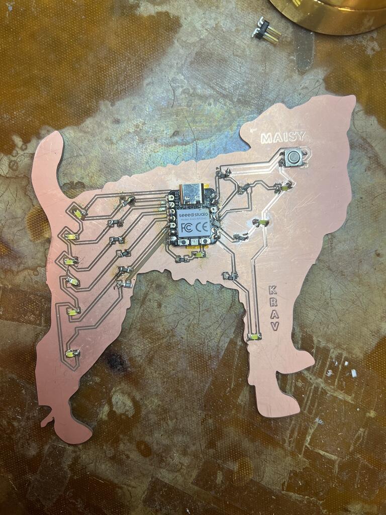
This was a really crazy week with Member’s Week directly into Labracabdra Hackathon Week and institute holiday in between, so I at least was definitely a bit on the back foot myself, especially since I had no experience with PCBs and little with soldering. Nonetheless, I had fun! (and made many mistakes, and suffered a tad, and learned a lot, etc etc)
GROUP ASSIGNMENT + TRAINING#
As usual Quentin bequeathed us with intense PCB wisdom. The takeaways I got are basically:
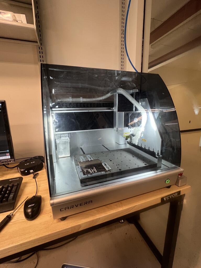
-we are very lucky and spoiled and should count our lucky stars and do a little dance that we get to use the Carvera (which costs ~$6000 dollars :o ). This machine makes it much easier than what students had to do in past in terms of auto leveling, tool switching and the like.
-
First step, secure the copper plate with the clamps so nothing moves during the milling process. You will need a sacrifical layer so the end mill doesn’t drill into the base causing problems and making everyone mad at you.
-
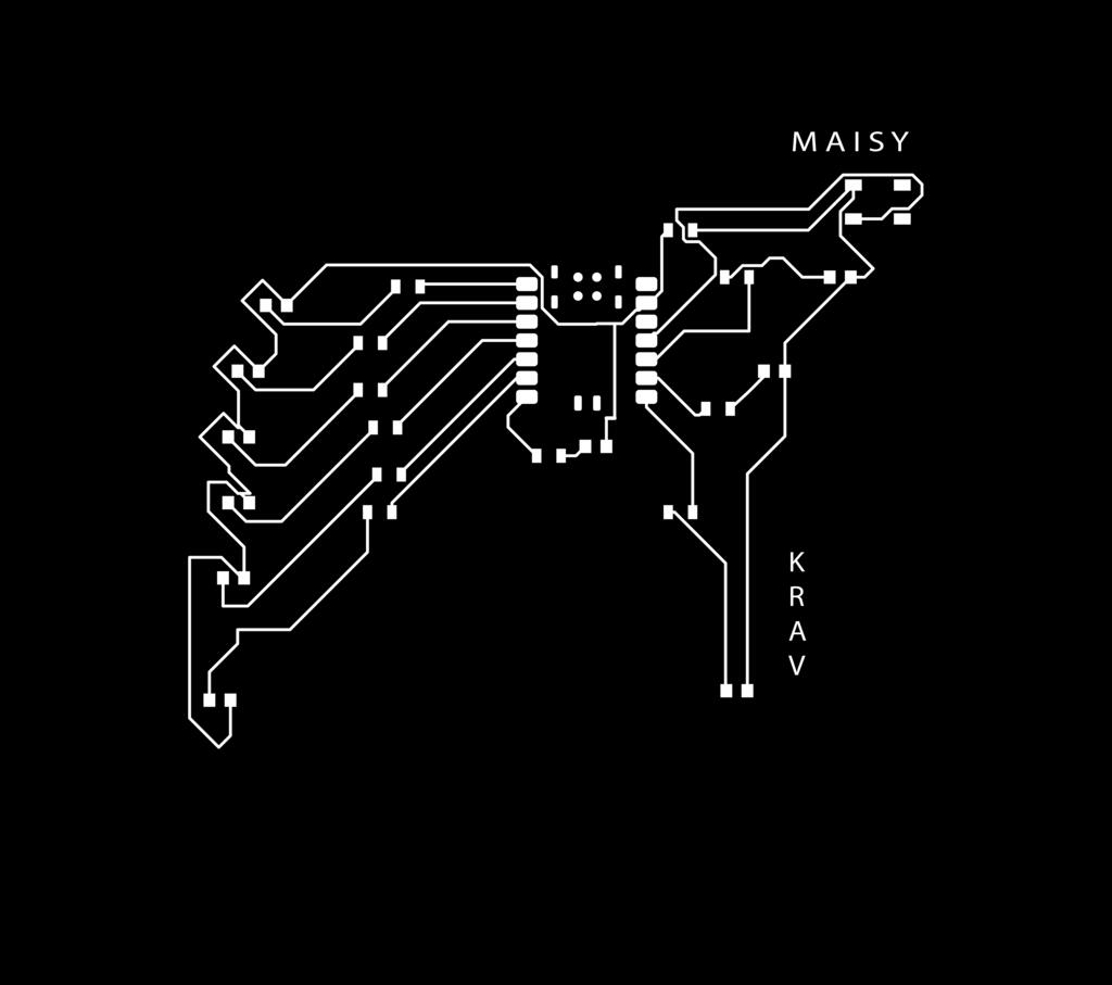
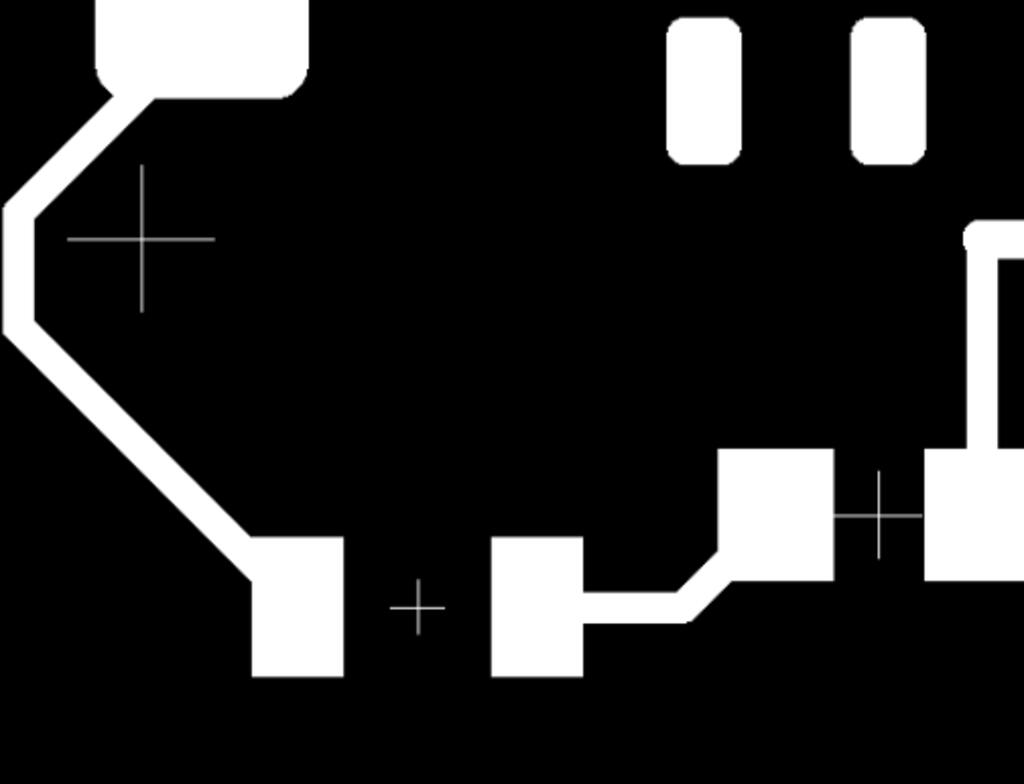
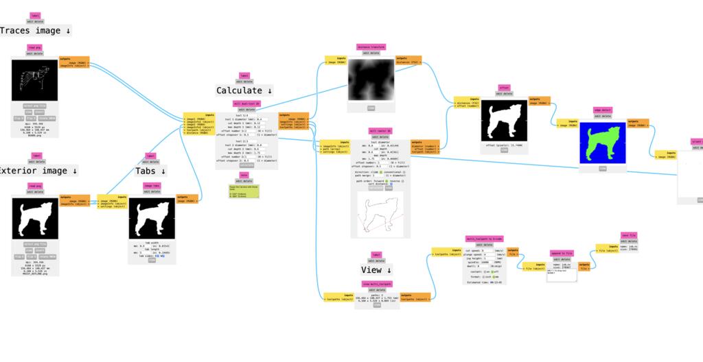
Go to mods (shoutout Quentin again for making it) and upload two pngs - the traces of your board (WHICH ONLY IS THE TOP LAYER AND NOTHING ELSE NOT EVEN CROSSES, this required me to make a few iterations where I made sure Fusion wasn’t doing any weird things with selection tools that added extra marks into the image). The second is the outline of the board shape. Both images need to be on top of a square or rectangle of the exact same dimensions so things don’t get hairy. These images must be monochrome. I did all of my silly silly png shenanigans in Illustrator, which you can read about more in Week 4
-
Add tabs - this should be very easy, but in my case since my board was weirdly shaped I needed to make them much longer than usual.
-
Hit calculate, and save the resulting nc file. I didn’t know what an nc file was, but basically it’s g-code, which is the language all machines that follow computer controls use, at least according to the source of all truth and wisdom that is Reddit.
-
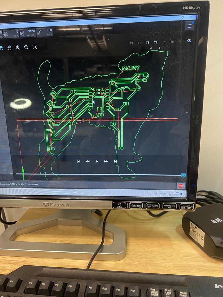
Load file into CarveraController, upload it, select it, and make your offsets are at least 5 mm from edges and other holes in board. Then hit run!
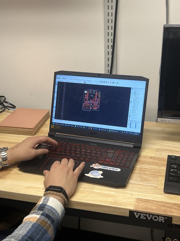
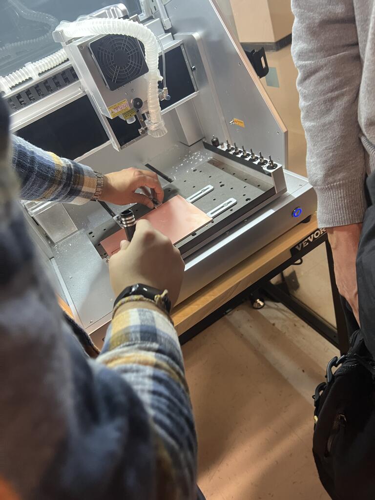
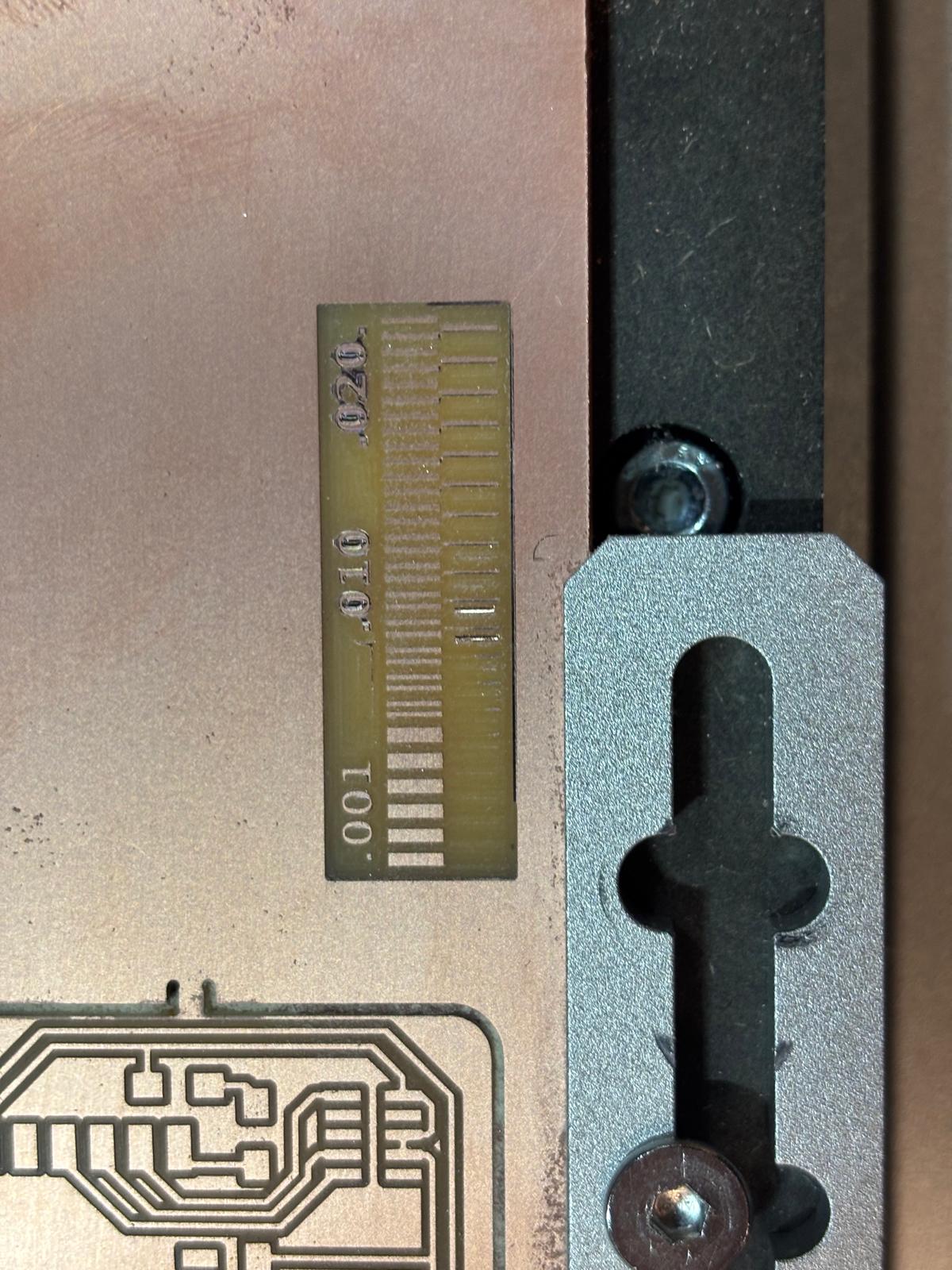
There was also the group assignment of seeing how far we could push limits of machine. We also designed a quick board and went through the steps of sending it off to be made in a board house.
MILLING DOGGY#
For me, since I wanted to do something quirky, I needed to pay extra attention to make sure I could get my funky dog shaped board I so yearned for.
I ran into a number of issues when trying to mill my board. First, I fired everything up then realized that the drill was about to destroy itself by going way out of bounds because my board was HUGE - like 15 inches. I was like uhhh this is bad, so the very first solution that popped into my head was oh I’ll just reduce my board by a scale factor which was a very silly idea! It did then mill (after a brief episode that Quentin told me is a bug where the laser does not probe on the second try, causing me to be scared that I broke something when it was just the machine), but it was waaay too small for anything to be used with it. (Thanks TA Marcello for helping me through this initial process!)
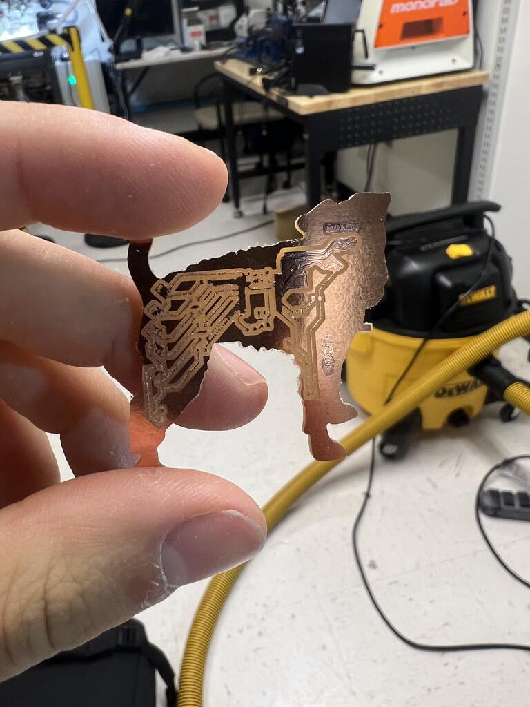
Failure number one.
I then got stuck because the machine refused to try again, telling me “ATM Tool Drop Fail” and stopping. I wasn’t sure what the issue was, but Alfonso happened to be around and we fixed it together by cleaning, recalibrating, and turning it on and off again. I also ran into some issues with bowing copper, but Alfonso’s suggestion of double sided tape worked great.
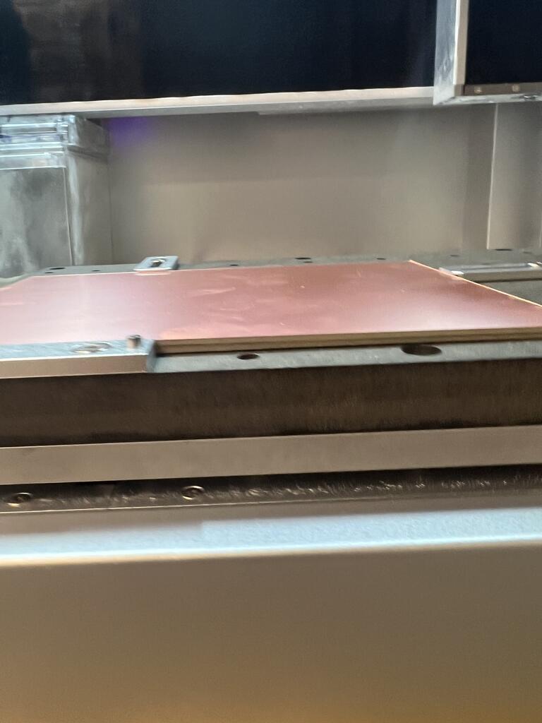
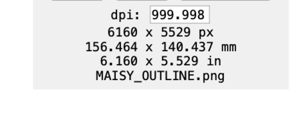
Then, after some messing around with my pngs and re-exporting them, I realized there was an error with Illustrator altering the ppi of my images. After fixing it (I used 1000), it was still pretty big (~5 inches), but Anthony told me it was ok. Plus, big pcb doggy is even better than small!! So it worked!!
SOLDERING = I CRI#
Then came time to solder - I did have some background with doing this, but nothing like this, and nothing in particular with surface mount components on a pcb.
TLDR: this was really hard for me :(
I personally really wish there was some kind of bonus training on soldering because it felt like I would make a dozen mistakes, cry, a extremely kind and helpful TA would take pity on my soul and offer a crucial tip, and I would improve but it felt like I needed all of this wisdom delivered before I started since I was so frankly bad at it. In fact, I messed up soldering so much that after a long period of trying to get the solder off all my shorted components I realized it would be faster to just mill another board, which I did.
At this point, I did manage on the second try after many tears and hours of trying to get something that vaguely resembled a microcontroller soldered on a board with a few components and a button. However, while the RP2040 worked, none… of my… parts… did, so I wanted to spend some time debugging why. My hope was to use the multimeter to debug as we were taught but it took me a silly amount of time to figure out what the continuity symbol was, but it proved quite useful once I did get it.
Soldering = pain, at least for someone bad at it like me. I initially had really “ambitious” goal of making a little glittery light show with a bunch of cute little LEDs, but I ruined at least one board with way too many shorts, and basically had a horrible time getting it to work so I settled for one functional blinking LED.
My stupidest mistake was having the resistors upside down and the LEDs flipped around, which caused me a lot of time and pain. It was made harder by the fact that the solder tip was super thick (in Quentin’s words, “this tip is dummy thic”)
I do feel like I learned so much though in terms of how to debug, use soldering tools etc so I am quite happy nonetheless~
SECRET DEBUGGING#
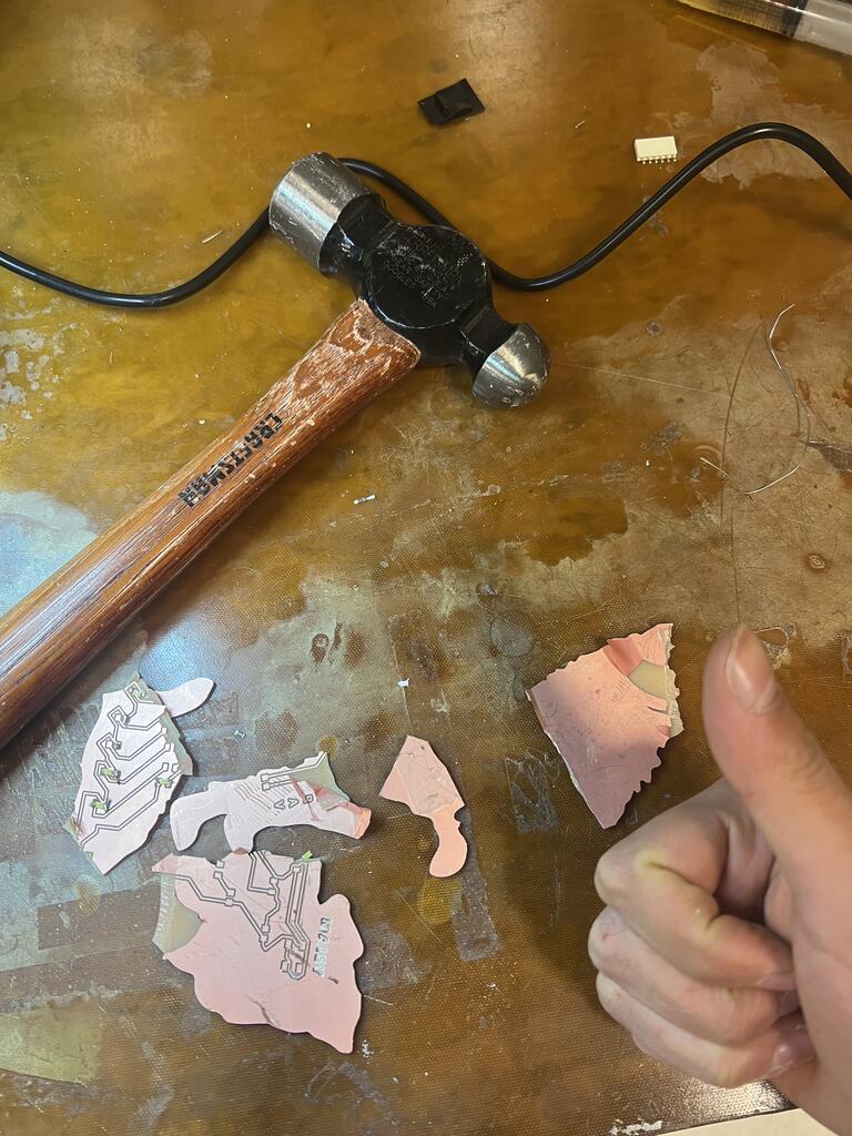
Also, for one of the boards I ruined, I used Anthony’s very excellent recommended debugging technique of Widlarizing, which totally fixed my problem and made me feel much better!
KNOWLEDGE THAT WAS VERY HELPFUL FOR ME THIS WEEK / QUESTIONS I WAS WONDERING THAT I GOT ANSWERS TO#
Q: What is "tinning"?
A: "Tinning means applying a thin layer of solder to your soldering iron tips. This protective layer prevents your soldering iron tip from oxidising. It also makes soldering easier, as the layer creates a heat connection between your tip and the part you are soldering, which increases the efficiency of the heat transfer." [Source](https://www.google.com/url?sa=t&source=web&rct=j&opi=89978449&url=https://www.vtech-smt.co.uk/blog/post/soldering-iron-tips-and-how-to-correctly-care-for-them%23:~:text%3DTinning%2520means%2520applying%2520a%2520thin,efficiency%2520of%2520the%2520heat%2520transfer.&ved=2ahUKEwiRu_HJ7pCJAxWlEFkFHTiZERUQFnoECBMQAw&usg=AOvVaw3QwB5VcGM7ihSX6tEqmFKb). Basically, this is when you add a little solder to a component to make it easier to join things later.

Anthony's recomended workflow for soldering components was: "Use the iron to "tin" a pad on the board (say one side of a resistor) with a nice little mound of solder
Now with the iron in one hand use your other hand to grab the part with tweezers.  Melt the solder with the iron, while it's hot place the part into the solder and then remove the iron and let it cool.  Solder the rest of the part before coming back and resoldering the first joint" - very helpful!!

Q: How do traces underneath stuff work?
A: Yes, this is ok - basically it seems that most components have an insulated layer on the bottom so this is generally no problem.

Q: Tape bottom of RP2040 why?
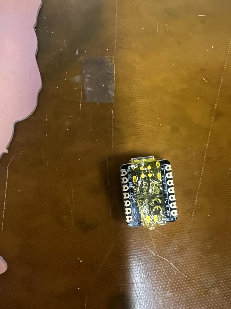
A: The bottom has a bunch of little debugging pins we don't need - you should use something like [kapton tape](https://en.wikipedia.org/wiki/Kapton) since it insulates. Otherwise you will short out your board.

Q: cathode/anode side of LEDs and things?
A: Yup, there is no standard because sure why not :) You need to check datasheet to see which side is CATHODE=goes to ground, ANODE=goes to power. As to what those terms actually are, "The cathode is the positive electrode, where reduction (gain of electrons) occurs, while the anode is the negative electrode, where oxidation (loss of electrons) takes place"

Q: uh this is a cool pcb board but what i am looking at what is actually conductive here? Is it the outline or the negative space?
A: Honestly this is a stupid question on my part, but my working understanding is that there are pads and traces, with traces being lines and pads being the bigger square bits where components go.

Q: How do I use a multimeter for debugging:
A: Covered in Anthony's recitation (linked below), but basically important things are "Check for continuity. If you have a continuity beeper on your meter, it'll beep when there's an electrical connection between the two probes. If you don't have a continuity function, just set it to a low level resistance setting and look for low resistance (e.g. 0 to 5ish ohms)", and.... "Check the voltage difference between two points, most often a specific spot in the circuit and ground. e.g. put one probe on a GND point, put the other on the power pin of an op amp and make sure it has the expected voltage." (https://www.reddit.com/r/diypedals/comments/12u10en/debugging_with_multimeter/)
Helpful tutorials I watched:#
and as always:
Notes for Progeny#
-This week, the TAs are owed an incredible thank you from me. I pestered them honestly a bit beyond what was probably reasonable, since I had very little background with this stuff and needed more help, but they all were so kind and helpful nonetheless.
-Spiral design good once again, things not working would have been x10 more painful if I had waited until trying to solder EVERY component
- Take more pictures of failures! When things go bad attitude should not be not work I cri but rather woah this is sick documentation :o
And Illustrator files