Networking
Inspired by my gadget grid attempt during big week, I attempted to make a grid of gadgets that are powered electrically and can send signals such as where the player is in the grid. I was planning to also add switch gadgets and have them detect the switch’s position (not actuate it, motors are expensive), but realized that there wouldn’t be enough time. So only wire and turn gadgets for now.
Frame the Gadget
The initial plan was to make a grid of frames that are connected electrically, and then gadgets can be placed on top of the frame. This has the advantage that gadgets can just be picked up from the frame no matter where they are.
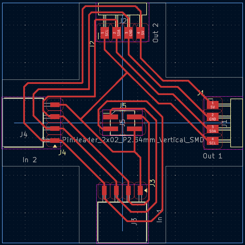
It’s important to select which wires will be in the frame, connected to all the gadgets. We obviously need power and ground. Then we need communication, which will be one big I²C network with all the gadgets as peripherals. That’s a total of 4 lines: VCC, GND, SCL, SDA.
In addition, it’s important to make sure these frames can tile the grid and that headers and sockets line up.
There are several frame designs to choose from. I chose the one on the left in the above tessellation examples because it’s easier to wire. Now, wiring!

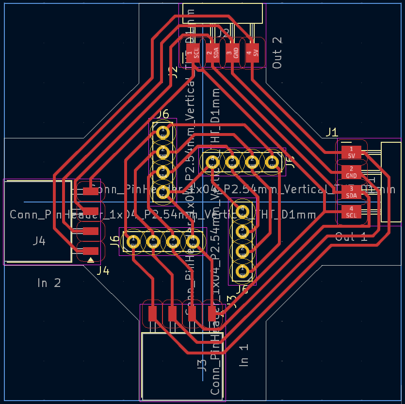
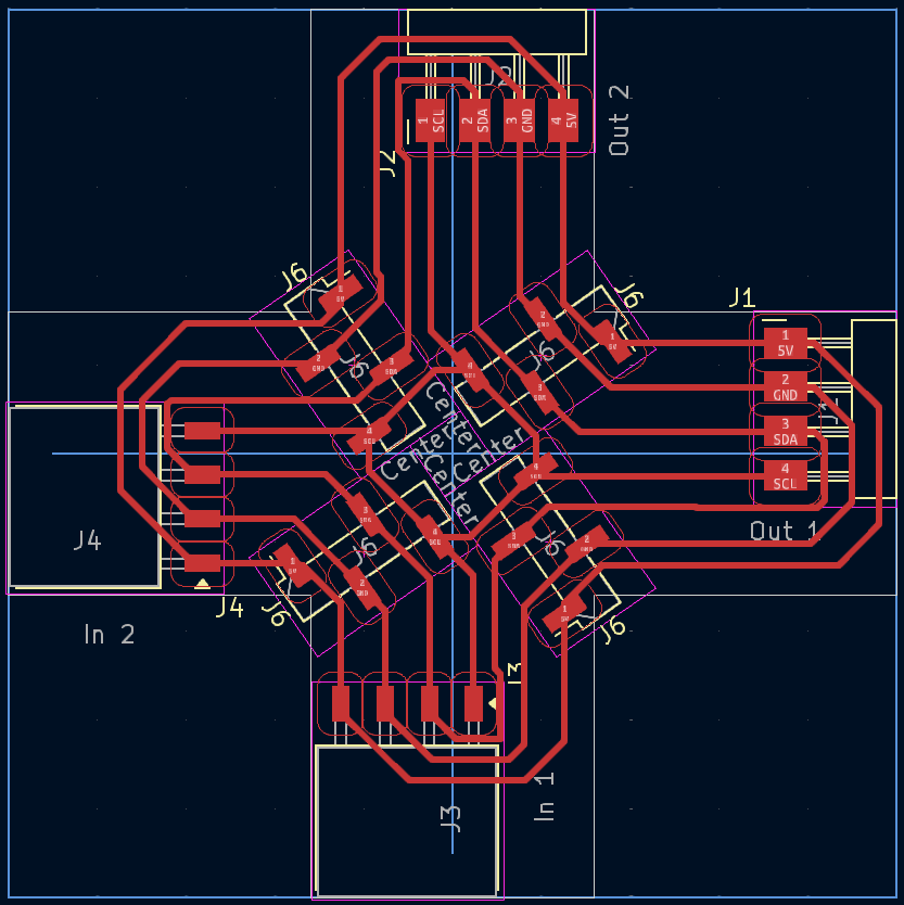
The center needs 4-way rotational symmetry, blowing up the number of pins required to 13 (I used 16 to simplify things). This made wiring a lot more cramped, as you can imagine. I set the design rule clearance to 0.8mm to avoid having to pull out the time-expensive 1/64” end mill.

After milling and soldering this, it turns out that soldering through-hole pins is annoying because they just want to fall out while you’re trying to solder them. So I switched to surface-mount instead. What could go wrong?

Talk the gadget
Before we get to the gadget board, we should come up with how the great I²C interface will be used to actually allow gadgets to communicate. Unfortunately while thinking about this, lots of problems came up:
- The ATtiny1624, which I used for this assignment, has only 1 I²C interface. Given that a gadget is connected in 4 different places, it needs to handle that somehow.
- If you try to just mux the pins so that only one of them is connected to the gadget at a time (and then make them take turns), there are several problems:
- It requires like 32 MOSFETS, making it more expensive than even a Raspberry Pi Pico (if you use fab inventory MOSFETS.)
- I haven’t figured out how to do a bidirectional mux that doesn’t break if an inactive line tries to communicate (by, according to Falstad, producing reverse flow across a MOSFET).
- Giving each gadget a unique address at runtime is hard
- Breaking the initialization symmetry is the tricky problem
- Yes, you could wire (or program) different addresses, but then you need to make sure you don’t accidentally give multiple gadgets the same address
- A gadget would like to notify the controller if the player reached its location.
- which means that “gadget = peripheral” doesn’t work.
- Multi-master I²C, while supported by the ATtiny1624, is full of hairy problems
So instead of one big I²C interface, I went with neighbor-to-neighbor communication. Which has the problem that now I have to figure out how to receive from 4 different places, but I don’t need to worry about unique addresses (there’s no symmetry when the positions of the gadgets actually matter)
Items
Prototyping the player
- friction
- torque
- prototype 1
- inward feet
- track width parameter needs to be tiny
- friction caused by torque is too high
- prototype 2
- wheel feet
Acrylic flatness
- thickness tolerance
Frame Board
- support gadget rotation
- first iteration didn’t
Gadget Board
- lot of complications
- supporting the pins (sockets?) to the frame
- programming the ATtiny
- only 1 I2C interface
- bidirectional muxing is hard
- connections to track lines
- communication
- I2C is hard
- Arduino doesn’t have an easy read-from-register function
- Giving each gadget a unique address is hard (Hall sensor flashbacks)
- multi-master is hard
- race conditions
- every gadget requests an identifier from the main board at the same time
- I2C is hard
- neighbor-neighbor communication
- receiving from 4 places is hard without hardware support
- first double-sided board
- asked about good hole size, got 39 mills
- climb vs. conventional milling (climb good, conventional super burry)
- stars
- they’re chiral! Beware the orientation
- programming
- lots of settings to set: programmer, port, board
- fast-switching diode ≠ Schottky diode. (thanks https://github.com/SpenceKonde/megaTinyCore/issues/545)
- used 4.7K Ω resistor instead
- make sure to select the exact chip!
- assembly
- https://forum.arduino.cc/t/progrsmming-arduino-with-assembly/397708/6 (gotta have that capital S file extension)
- clocks might be a bit too varied…
- interrupts
- https://www.ojisanseiuchi.com/2024/03/03/a-quick-word-on-attiny-1-series-interrupts/
- message queue
- receiving is hard
- possible deadlock if you try to transmit multiple messages before dequeueing a message from the receive buffer
- timing of message receiving is important
- probe connected to message clock trace at startup kills interrupt-at-start bug.