Week of Oct 9 2024
Make and test a self-designed microcontroller board, characterize design rules for your lab's in-house PCB production process, and submit a PCB design to a board house
1. Group training on milling and soldering
The learning curve for this week was steep. First we underwent training on how to mill a printed circuit board (PCB), and how to solder. The steps for milling a PCB were as follows; the architecture fabrication shop's tutorial (https://archshops.mit.edu/modela.php) was a useful resource too.
- Ensure a clean milling base by vacuuming all debris.

- Taking a copper board from the stack between the 2 PCB machines (Roland SRM with cover to the left, older uncovered MDX-20 to the right), apply 3-4 strips of double sided tape from the dispenser zip-tied to the same table.
- Line up the right-angled edge of the copper board to the bottom left corner of the PCB machine's copper plate.
- Open up the PCB linux mods by entering "mods.cba.mit.edu/oldindex.html" as the linux browser address, and follow the steps on aforementioned Archshops tutorial, i.e. right-click on the CBA icon, choose programs > server program > Roland mill > srm20 > PCB PNG.
- On the linux mods interface, click on "move to home" so that the mill head rises up to a height conducive for changing mill bits.

- Retrieve 1/64 (for traces) and 1/32 (for outlines) mill ends from the plastic drawers on the wall to the right of the PCB machines

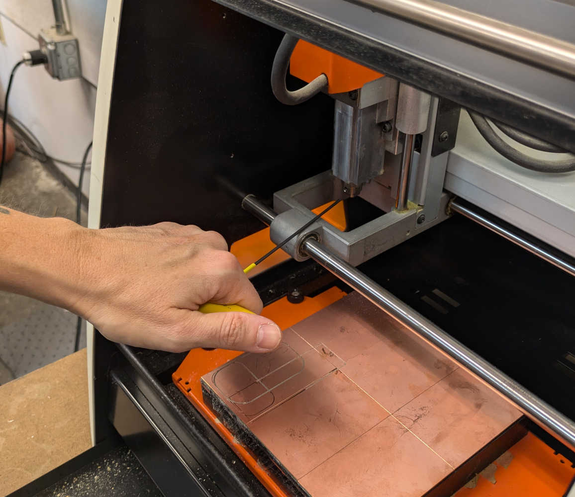
- Very carefully retrieve the 1/64 mill bit, DO NOT DROP IT as they shatter once dropped and are expensive to replace. Use the yellow T-handle hex key located in the drawer on the bottom of the Roland PCB milling machine to loosen the "collet"/ mill bit holder, and using your finger to cushion the 1/64 mill bit, insert the mill bit into the collet and tighten it with the yellow hex key.

- Make sure the mill bit protrudes sufficiently past the collet, per diagram (drawn by our TA Diana).

- On the mods interface, set z to 15, and x and y to desired start point of your mill. Click "move to origin" to move the mill bit to the specified location, and make microadjustments to x and y until the mill bit is at your desired start location. Then slowly lower the mill bit by gradually reducing the value of "z".
- Keeping your finger on the mill bit to control its descent, use the yellow hex key to loosen the collet and let the mill bit gently descend until it touches the surface of your copper board. Hold on to the mill bit as you tighten the hex key (since it tends to ride up a little during the tightening process if you don't hold on to it).
- Going back to mods, click on "mill traces" > "calculate" (under "Mill raster 2D") > "send to device" (under "Websocket device"). This should start the milling. [Troubleshooting: If the milling doesn't start, check if the green light on top of the Roland PCB machine is blinking, as it means there is an error. Turn the PCB machine off and on again and wait until the green light holds steady - as long as it doesn't blink, the print job should go through.]
- Vacuum when done with milling, and repeat steps 5 to 11 but with a 1/32 mill bit, and by clicking on "mill outline" instead of "mill traces". [Troubleshooting: if the milling of outlines doesn't start, check if a mill path has been generated when you hit "calculate", and if not, try inverting your png, until a mill path generates.]
The design rules for the architecture fabrication shop's PCB mills were as follows:

The steps for soldering were:
- Wash your milled PCB with the orange pumice handsoap located in the room next door. Oily PCBs make it difficult/impossible to solder.


- Turn on ventilation fan (turqoise box), soldering iron (setting to ~75-80, i.e. on the hotter end, makes for easier soldering), and the light on the magnifying glass. Useful to tape your PCB down onto a piece of cardboard and to tape it to the table.

- Put the soldering iron on the point you want to solder, and place the tip of the solder onto the iron, like so. You can clean the soldering iron on the gold mesh attached to the solder holder between solders.
2. Make and test a self-designed microcontroller development board
With guidance from TA Anthony on my PCB design from last week and assurance that I was connecting to the right things (i.e. it is correct to connect the 3.3V and 5V power sources separately to intended input and output ports), I switched out the footprint of my microcontroller for direct mounting (rather than drilling holes) and added a tactile switch and LED to facilitate testing. While it took me hours to complete the earlier round of simple routing, I was able to route this redesigned board relatively quickly - growth!


Design file link to the Fusion Eagle schematic document and PCB layout for my second PCB.
The Eagle software (integrated with Fusion, hereon referred to as Fusion Eagle) has a few quirks, one of which is that when you are trying to make a copy of a file, you need to open the schematic (and not the PCB or combined document), before saving it as another filename to make a copy of the full set of 3 documents (schematic + PCB + combined). So always open up the schematic document (icon in red arrow here; the many copies before indicate my failed attempts at copying files). [Edit as of Dec 18: Open the last file with two icons combined instead of the schematic. Subsequently I found that opening that last file format more consistently allowed me to successfully copy Fusion Eagle files.]

As I started milling right after TA Diana's training, the steps were still fresh in my mind. Note to self: it is helpful to immediately try something out after learning, rather than waiting a day or two and referring back to notes. But alas, my first mill was an immediate fail as the board shifted despite having added 3 layers of double-sided tape underneath. This was probably due to me not pressing the copper board down, so for the next mill I added another row of tape and pressed it down. I was initially afraid of making the plate oily with my fingers by pressing it down, but then remembered that the oiliness only mattered at the soldering stage later, and not now at the milling stage.

The next issue was the print job not sending to the mill. It turned out that a blinking green light on the mill meant that the mill was not ready/ was experiencing connection errors. Together with shop expert Shah, we found that turning off and restarting the mill (by either holding down on the green button, or unplugging the cable altogether and plugging it back in), until the green light was a steady one without blinking, allowed the mill to start printing. The trace milling went well, but my next failure was the board outline not milling. After some troubleshooting with shop expert Shah, we realized that I had to invert the colors of my png in order for the outline's mill path to be calculated. Note to self: the milling will only work if the trace path has been successfully calculated!


After resolving these issues, I finally managed to finish milling my first PCB. I was a little worried when the outline mill made additional passes drilling on on the outer edges, but my guess is that it was automatically done to make it easier to release the PCB.

The next step was to locate the components for soldering. I struggled with finding the right components, and found that frequently referring to the class inventory and searching up data sheets of the corresponding components helped. In particular, I had to carefully distinguish between a 10k ohm and 10 ohm resistor (pictured below), finding the correct 4-pin rather than 2-pin tactile switch (which were not located in separate labelled boxes but in the same box, just in different ziplock bags).


In figuring out which direction to connect the components, I looked at the data sheet of the specific LED component I used, and learned that the "cathode mark" (which is the green strip in the picture below) corresponds to the negative end of an LED, which then connects to ground. A quick online search also taught me that resistors were direction-agnostic.

I quickly found that soldering was much less straightforward than I imagined. Despite hearing that lead-based solders were easier to solder than lead-free solders, I chose to prioritize my lifespan and persisted in my struggle with the finicky lead-free solders - which took a longer time to heat up, and dried up rapidly. I also quickly abandoned my earlier plan of soldering my XIAO RP2040 board on in a plug-and-play way, and decided to solder it on directly, to simplify and reduce the number of solder joints.

The solder pads were also too small for me to attempt to solder on the available connector pins (2 x 3 header connector, alternating legs), so I would have to amend the PCB png and mill it with larger solder pads in future for a plug-and-play connection.

Following TA Anthony's guidance, I also taped up the middle connection points on the back of the SEEED board to avoid any contact with copper on the PCB.

The next issue was realizing that the milling of traces missed out on an entire line, leading to all my solder pads on the right side being interconnected. Board surgery was then in order - I used a pen-knife to scrape off excess copper, making sure to cut in a way such that if the blade slipped, the copper removed would not be consequential. The before and after are as pictured.


Carried out a continuity test using a backlit board/ phone light.

Next was to test for continuity to make sure that the components were all well connected. I used multiple multimeters and switched it to resistor (ohm) mode to check for beeps (beeping = circuit is closed).


I spent some time resoldering components that did not register a beep, and spent the most time fixing the LED. I soon realized that my repeated soldering and reheating (in an attempt to fix cold joints) effectively burnt the LED, so I tried to remove it by smashing it and pulling it away, and soldering on a new LED. I also found that leaning the solder on the component and using the soldering iron to "push" the heated solder onto the component worked best. And to fix cold solder joints, I found that in addition to reheating soldered parts, it helps to introduce new solder, so sometimes that entails scrapping existing solder away.


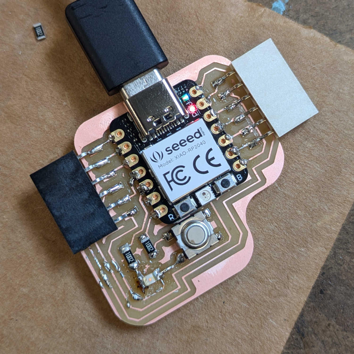
Connected the completed PCB onto my computer, and downloaded the latest version of Arduino IDE. Realized that the USB cable matters - the top cable is a data-transfer cable, while the bottom is a charging cable. Only the former will work.

When successful, the SEEED XIAO RP2040 will register on a Mac laptop as follows:

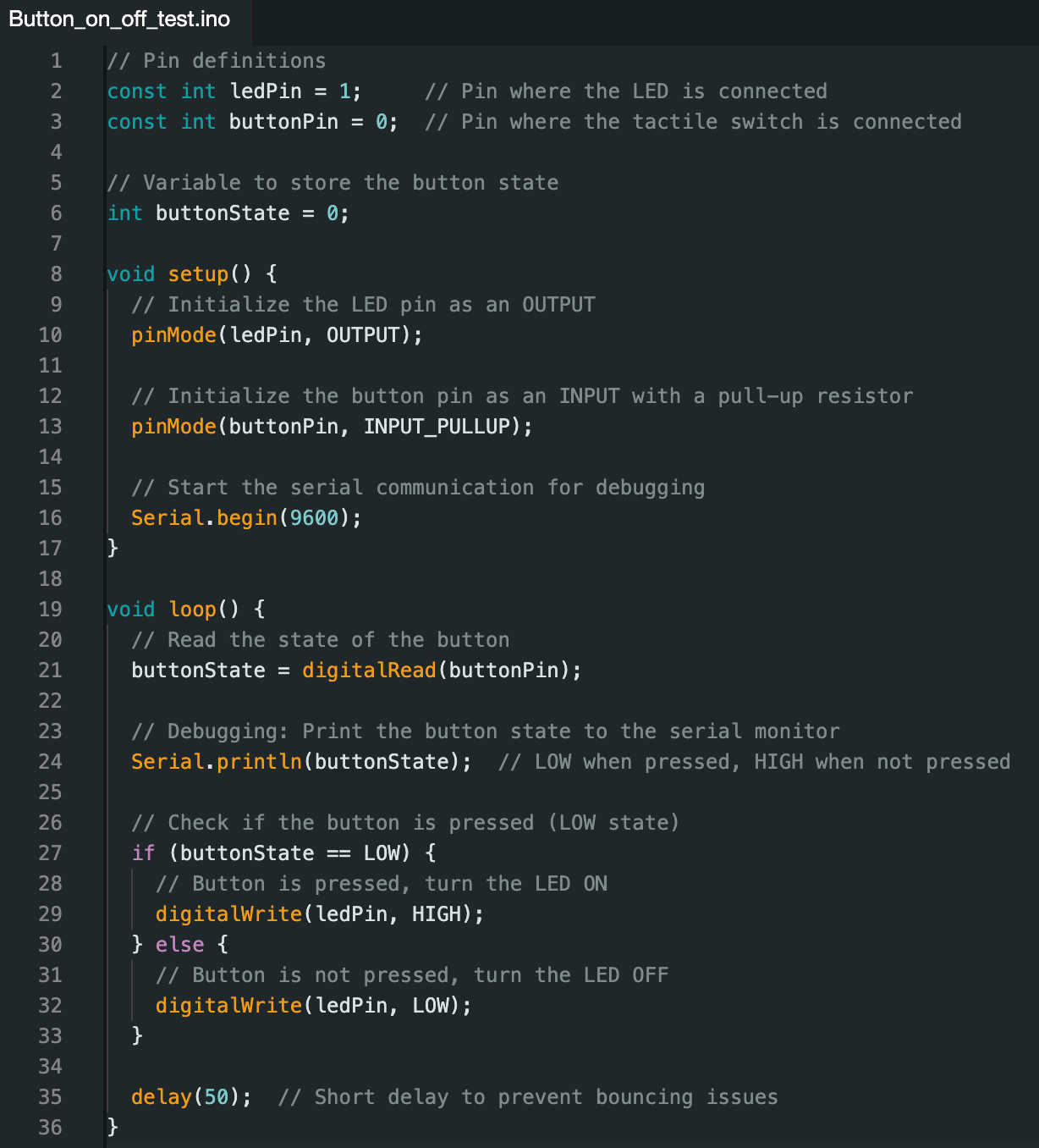
Now that the PCB is connected to Arduino IDE, I opened up example code from within the Arduino IDE itself - I picked the default "Button.ino" option to test the tactile switch and LED. Upon changing "INPUT" to "INPUT_PULLUP" (through consulting ChatGPT) and modifying the pin numbers to match the connections on my PCB, the LED lit up!

The top image shows the LED off (see bottom left of PCB), and the bottom image shows it on.


After troubleshooting with TA Anthony, it turns out that I should have used a 1k instead of 10k ohm resistor. The calculations are as follows, with the "Vf = 1.3V" and "Imax = 0.02A" values retrievable from the components' data sheets. I also learned that the addition of "PULLUP" activates a pull-up resistor which ensures that the starting voltage is constantly at 3.3V instead of being drawn from random electric signals; i.e. it maintains voltage because there is no voltage delta.

In consultation with ChatGPT, I isolated components to test. First I tested whether the tactile switch works, using the following code. If the tactile switch works, the serial monitor in Arduino IDE will display "1s" when pressed and "0s" when not pressed.

It worked!
The next test was on the LED, using the program below.

This did not work, so I went to consult TA Anthony for further troubleshooting. He tried a few things - using a tweezer to short between a resistor (to fix the existence of my 10k ohm resistor that was dimming the LED too much). It didn't work, so he tested continuity using a multimeter. To check voltage, he connected the black probe to ground, red probe to 5V pin (V should read 5.5), 3.3V pin (V should read 3.3). If these 2 readings register, then we can be sure the meter is working well.
Next, TA Anthony showed how one can connect the red probe to anywhere else given that there is a pull-up resistor function so it SHOULD read 3.3V. However, my PCB did not read that, so he suggested for me to switch out my XIAO board entirely with a different one.
Since there were a few other things I wanted to fix too, I have summarized the following things to improve for a future PCB attempt, in terms of PCB design (to adjust before milling my next PCB):
- Increase pad widths so that I can solder on 3-head double sided connectors (to allow for plug and play)
- Widen board outline to accommodate 6-pin connectors
- Change 10k ohm resistor to 1k ohm resister so that the LED can be brighter (suggestion by TA Anthony)
- Increase distance between routes on right side so that I don't have to do board surgery again
- Perhaps follow LED circuitry in Arduino IDE examples?
Till the next PCB attempt!