Week 7 - Input Devices Group Assignment Summary
Probing Analog and Digital Signals from Various Input Devices
Assignment Overview
This page summarizes the group assignment for Week 8, focusing on probing input devices' analog levels and digital signals. We systematically investigated load cells, microphones, and IR phototransistors to understand their signal characteristics and measurement techniques.
Group Assignment: Probing Analog and Digital Signals
Three focused investigations: load cell (analog vs amplified digital), digital microphone (16 kHz clocked), and IR phototransistor (analog). Each subsection includes probe setup, scope captures, and brief interpretation.
Signal Analysis Overview
Comprehensive analysis of input device signals to understand analog and digital signal characteristics, measurement techniques, and practical applications in embedded systems.
Reference Materials
Source: MIT HTMAA Week 7 Group Assignment
Detailed documentation of input device signal analysis and measurement techniques
Key Signal Analysis Parameters
- Load Cell Analysis: Wheatstone bridge differential output vs HX711 amplified digital interface
- Microphone Signals: 16 kHz clocked digital output with synchronous data capture
- IR Phototransistor: Analog voltage changes with illumination intensity
- Signal Processing: Analog-to-digital conversion and signal conditioning techniques
- Measurement Tools: Oscilloscope operation and probe setup for accurate signal capture
- Data Interpretation: Understanding signal characteristics and practical applications
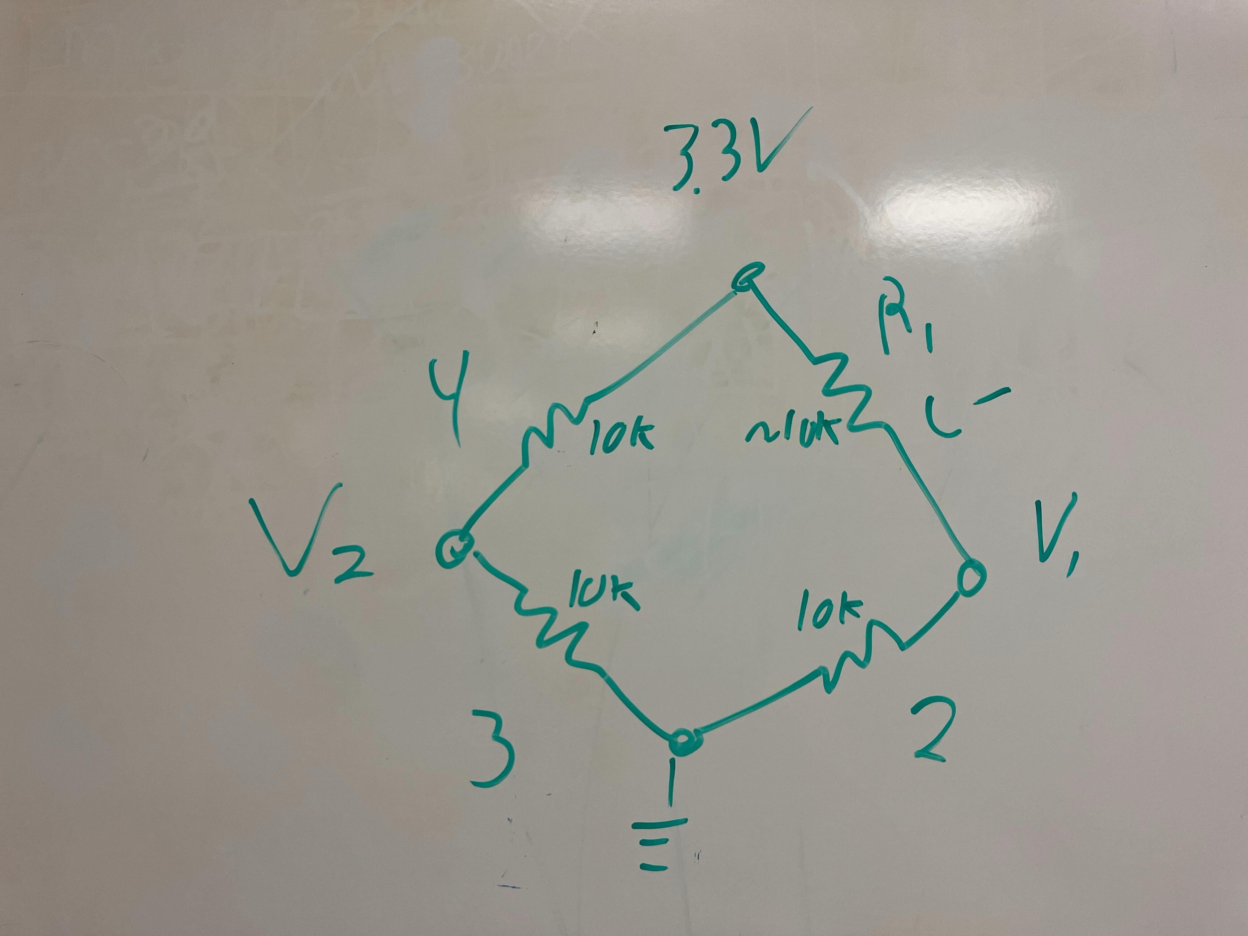
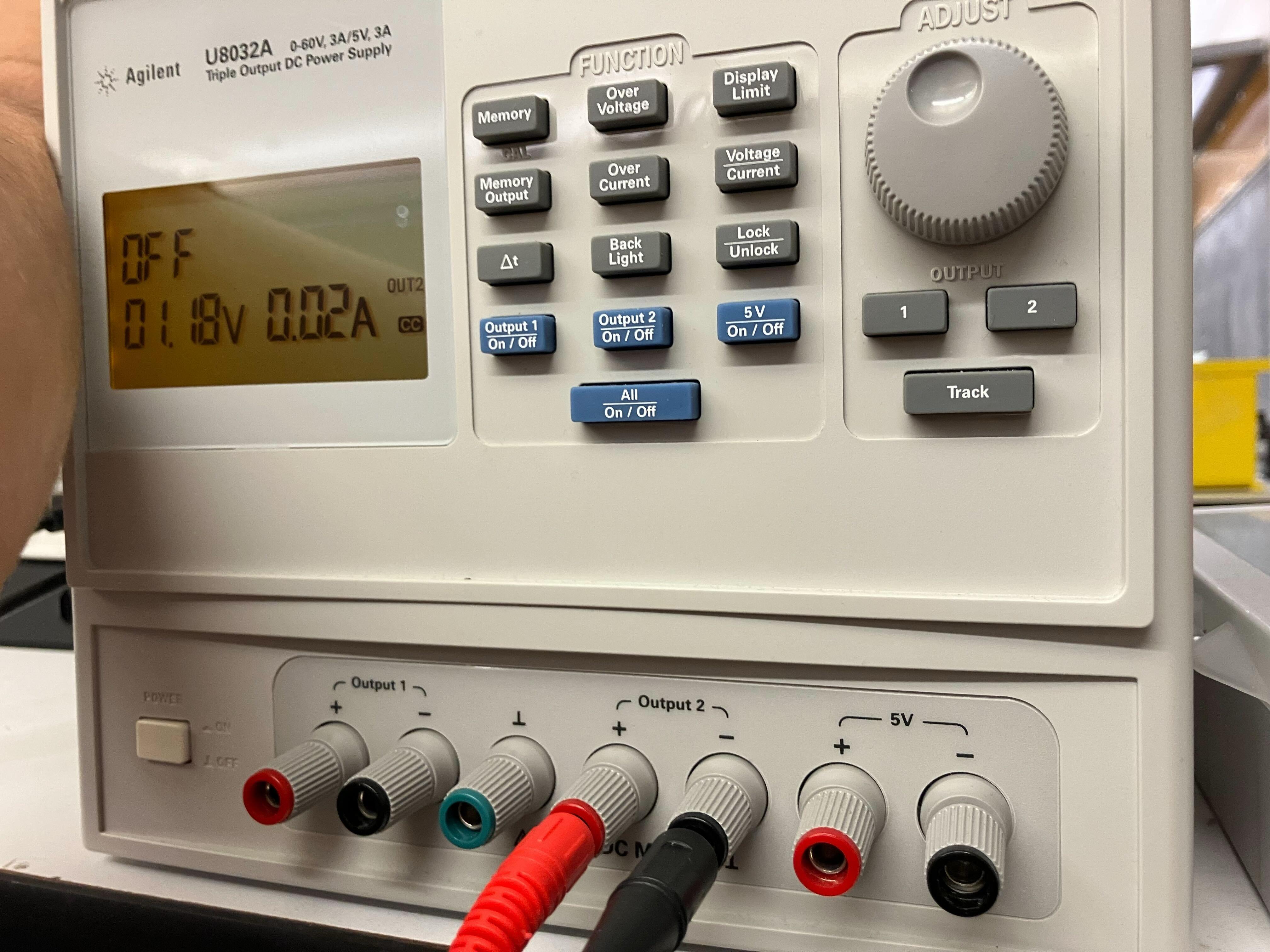
Load Cell: Direct Analog Output and HX711 Digital Output
We compare the raw Wheatstone bridge differential output to the HX711-amplified, clocked digital interface.
Why an amplifier board is needed
With a 3.3 V reference, the ADC step size (LSB) is 3.3 V ÷ 2N. Load-cell bridge outputs are only millivolts, so low-resolution ADCs can't resolve changes well.
- 8-bit ADC (N=8): ~13 mV per LSB (3.3 V ÷ 256)
- 10-bit ADC (N=10): ~3.2 mV per LSB (3.3 V ÷ 1024)
- 12-bit ADC (N=12): ~0.8 mV per LSB (3.3 V ÷ 4096)
At minimum, 12-bit ADC is needed to read the raw bridge signal directly on a microcontroller; a dedicated amplifier + ADC (e.g., HX711) increases gain and effective resolution, improving SNR and measurement fidelity.
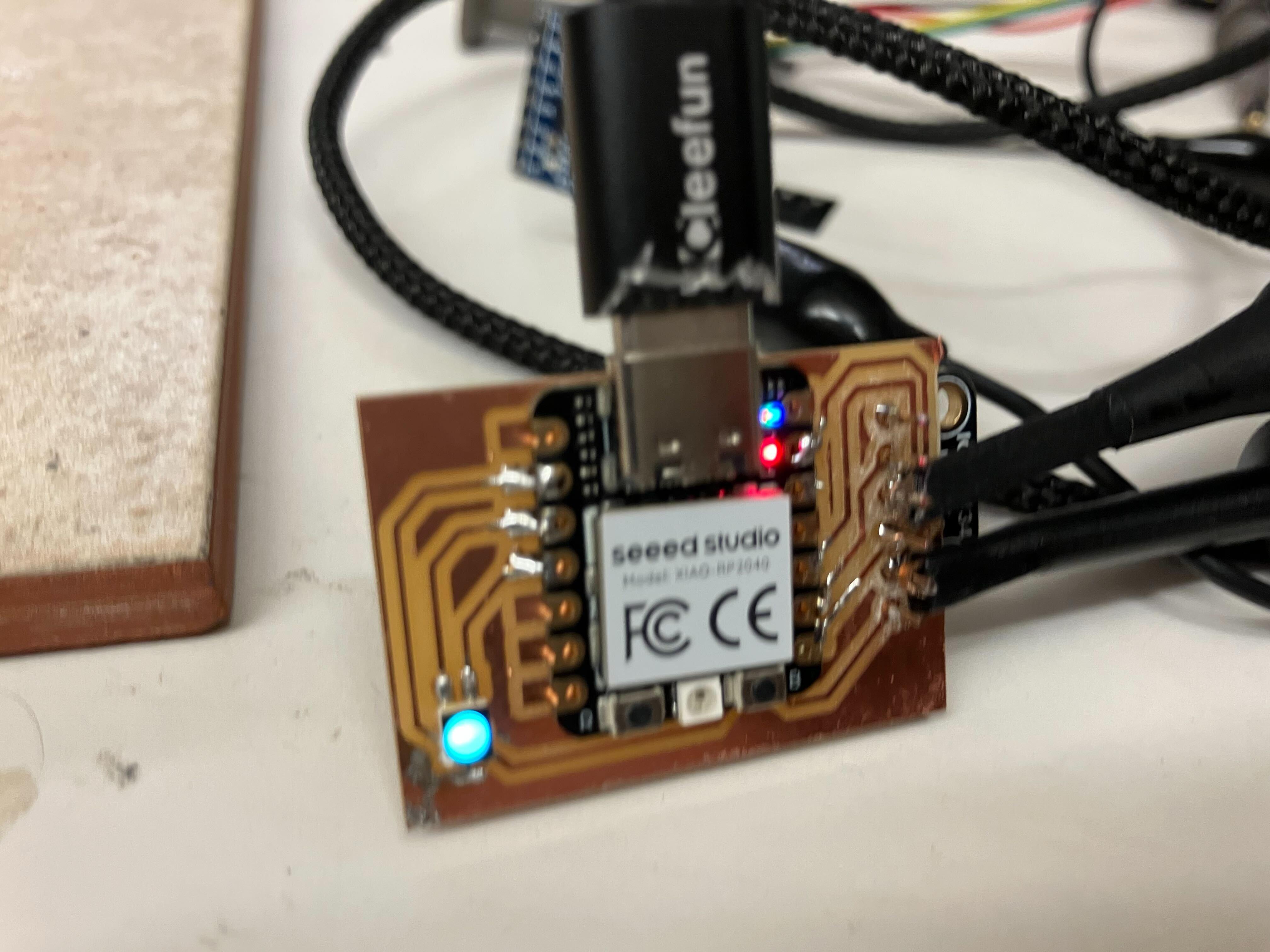
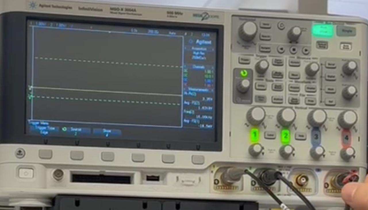
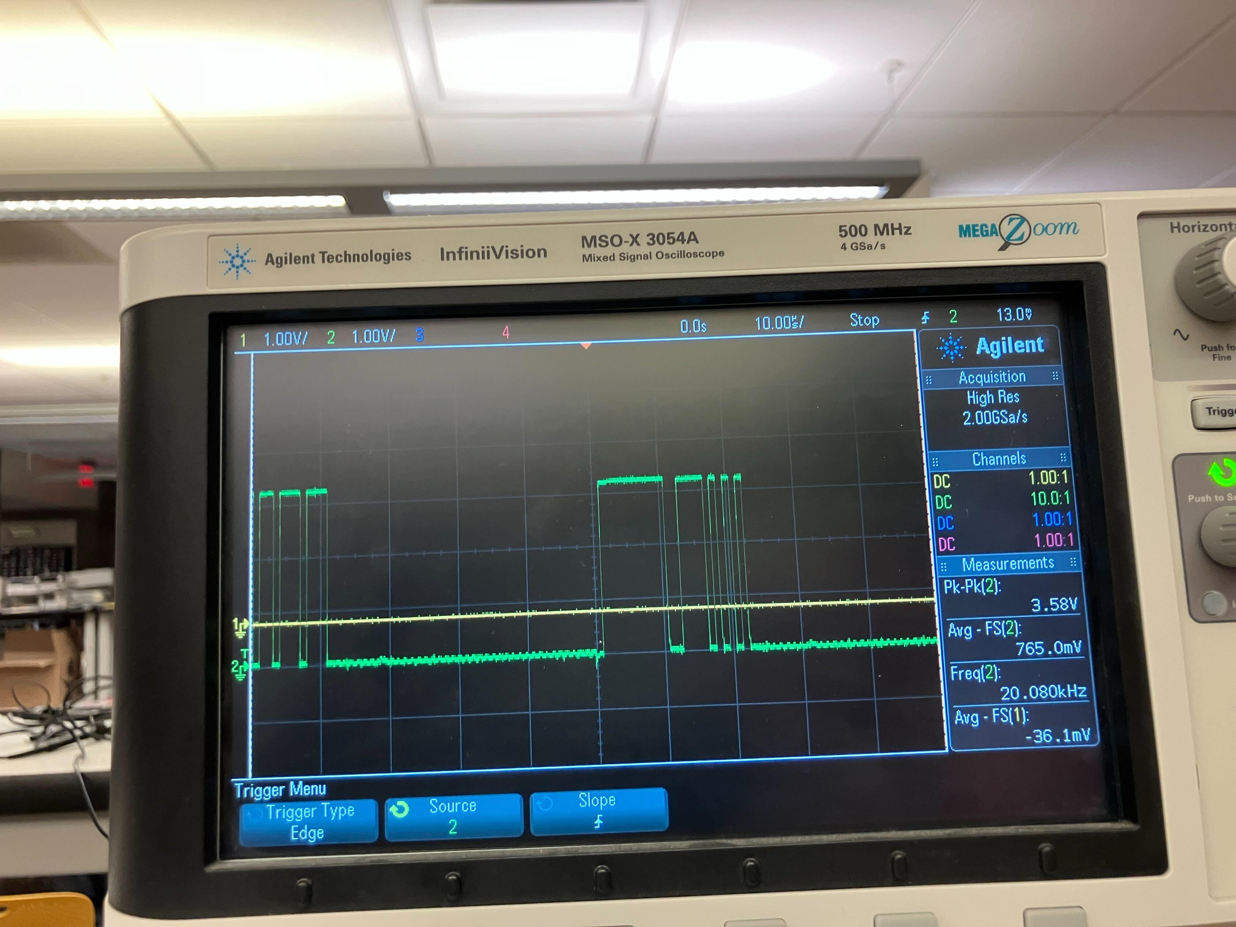
Microphone: Digital output with 16 kHz clock
We capture the probe points, the ~16 kHz clock, and the synchronous data output.
IR Phototransistor: Analog output
We power the IR emitter, probe the phototransistor node, and observe analog voltage changes with illumination.


Full Assignment Details
For complete details on the Week 7 group assignment, including comprehensive input device signal analysis, measurement techniques, and detailed results, please visit the full assignment page.
🔗 View Full Week 7 Group Assignment DetailsSpecial Thanks to Our Section
We would like to express our sincere gratitude to all members of our section for their invaluable collaboration throughout this group assignment. Your contributions were essential to the success of this comprehensive input device signal analysis project.
Collaboration Activities
- Signal measurement and oscilloscope operation
- Input device testing and characterization
- Analog and digital signal analysis
- Measurement technique documentation
Knowledge Sharing
- Oscilloscope operation and probe setup techniques
- Signal processing and measurement methodologies
- Input device characteristics and applications
- Embedded systems signal analysis
This collaborative effort demonstrates the power of teamwork in technical education and hands-on learning. The collective knowledge and shared experiences significantly enhanced our understanding of input device signal characteristics and measurement techniques.
References
- Input Device Signal Analysis
Comprehensive guide to analog and digital signal measurement techniques - Oscilloscope Operation
Professional measurement equipment usage and signal capture methodologies - Sensor Integration
Best practices for integrating various input devices with microcontroller systems - Signal Processing
Analog-to-digital conversion and signal conditioning techniques - Embedded Systems Design
Guidelines for designing robust input device interfaces
Ethical AI Use
Documentation of AI tool usage for this week's group assignment summary and website development work.
Week 7 - Input Devices Group Assignment Summary Development
This session covers the development of the Week 7 page for the input devices group assignment, including content structure, technical documentation, and comprehensive coverage of signal analysis processes.
AI Development Documentation
Complete development transcript documenting the AI-assisted creation of the Week 7 group assignment page, including content structure, technical documentation, and website development process.
Key AI Activities
- Content Structure
Creation of comprehensive HTML structure for input device signal analysis documentation - Technical Documentation
Development of detailed sections covering signal measurement and analysis techniques - Process Integration
Implementation of input device characterization and measurement workflow information - Navigation Integration
Addition of Week 7 link to main index page for seamless course navigation - Image Integration
Integration of key images and videos from week7groupassignment folder with proper styling and captions - Link Integration
Addition of external link to full Week 7 assignment details with proper accessibility attributes
AI Tools Used
- Cursor AI
Code generation, content structuring, and website development assistance - Technical Content Generation
Creation of comprehensive input device signal analysis documentation - Website Design
Implementation of consistent styling and responsive layout - Content Integration
Seamless integration of Week 7 content into Week 8 page structure - Media Processing
Integration and styling of images and videos with proper responsive layouts