![[Profile Image Placeholder]](profile.jpg)
Week 7
Input Devices
Week Highlights
Key captures from the group and individual assignments with links to their sections.
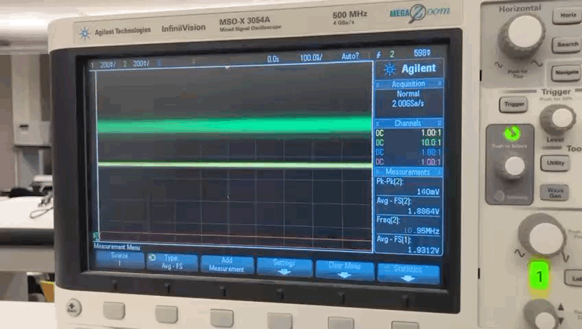
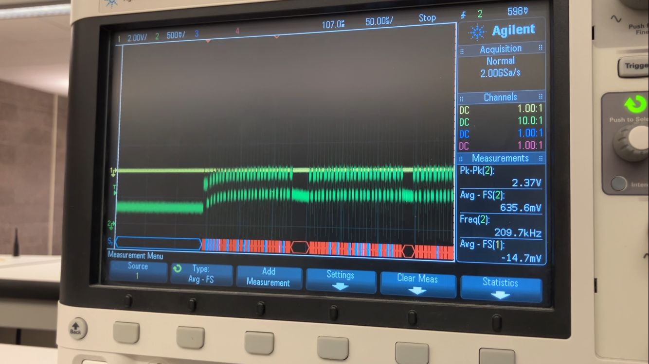
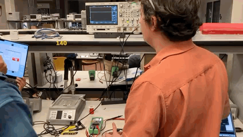
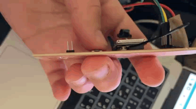
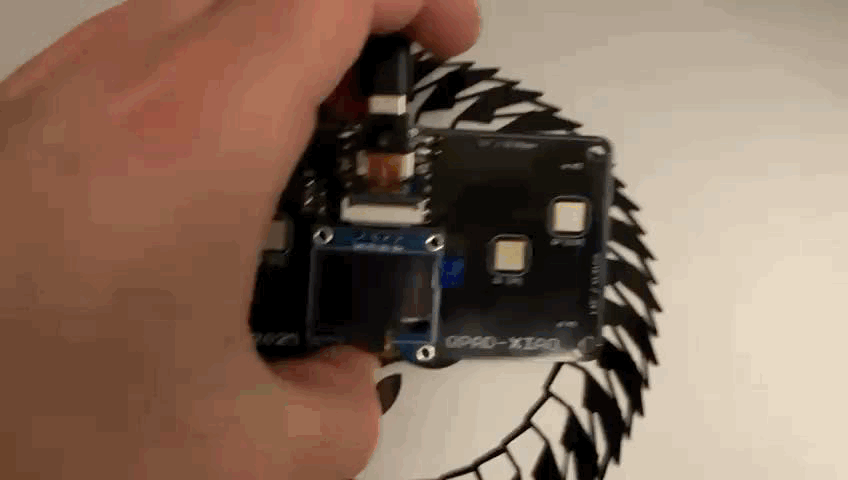
Table of Contents
Course Content
Training & Documentation
Input Devices
This week focuses on exploring various input devices and sensors that can be integrated with microcontroller boards. We'll learn about different sensor types, measurement techniques, and how to read sensor data.
This Week's Goals
- Explore Sensor Types
Learn about switches, magnetic field sensors, potentiometers, step response sensors, temperature sensors, light sensors, motion sensors, distance sensors, and more - Measurement Techniques
Understand analog and digital signal processing, filtering, and sensor calibration - Implementation
Add sensors to microcontroller boards and successfully read sensor data
Assignments
- Group Assignment
Probe an input device's analog levels and digital signals - Individual Assignment
Measure something: add a sensor to a microcontroller board that you have designed and read it
Tools & Materials
- Microcontroller BoardsVarious SensorsOscilloscopeMultimeterProgramming Environment
Training Documentation
Training materials and documentation for input devices and sensor integration.
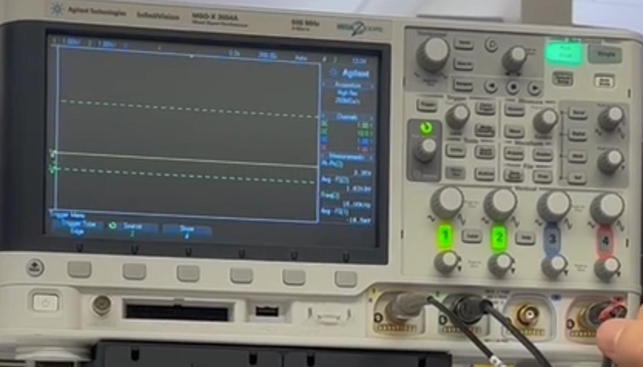
Oscilloscope Operation: Measuring Clock and Data
Demonstration of capturing a stable clock and synchronous data line, including probe reference selection and verifying edge alignment.
Combined capture shows stable clock and synchronous data suitable for decoding
Useful Documentation
Essential resources for input devices and sensor integration.
Class Page
Comprehensive resource covering all input device categories including switches, magnetic field sensors, potentiometers, step response sensors, temperature sensors, light sensors, motion sensors, distance sensors, and more. Includes detailed tutorials, code examples, and implementation guides for various sensor types.
Sensor Exploration
Exploring different types of input devices and sensors for microcontroller integration.
Sensor Categories
- Switches and buttons
- Magnetic field sensors
- Temperature sensors
- Light sensors
Applications
- Motion detection
- Distance measurement
- Environmental monitoring
- Touch interfaces
Group Assignment: Probing Analog and Digital Signals
Three focused investigations: load cell (analog vs amplified digital), digital microphone (16 kHz clocked), and IR phototransistor (analog). Each subsection includes probe setup, scope captures, and brief interpretation.
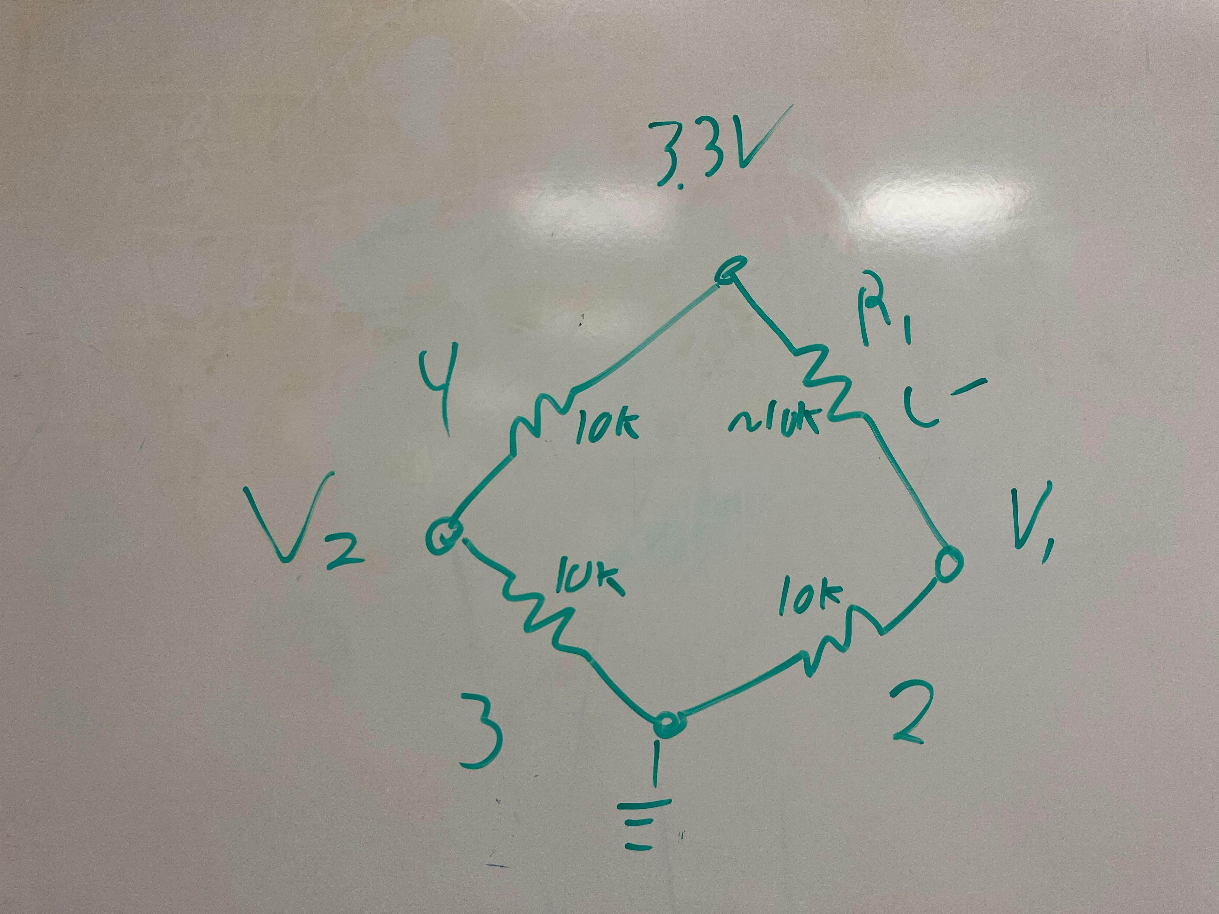
Load Cell: Direct Analog Output and HX711 Digital Output
We compare the raw Wheatstone bridge differential output to the HX711-amplified, clocked digital interface.
Why an amplifier board is needed
With a 3.3 V reference, the ADC step size (LSB) is 3.3 V ÷ 2N. Load-cell bridge outputs are only millivolts, so low-resolution ADCs can’t resolve changes well.
- 8-bit ADC (N=8): ~13 mV per LSB (3.3 V ÷ 256)
- 10-bit ADC (N=10): ~3.2 mV per LSB (3.3 V ÷ 1024)
- 12-bit ADC (N=12): ~0.8 mV per LSB (3.3 V ÷ 4096)
At minimum, 12-bit ADC is needed to read the raw bridge signal directly on a microcontroller; a dedicated amplifier + ADC (e.g., HX711) increases gain and effective resolution, improving SNR and measurement fidelity.
Direct analog output
Probing V1 (green) and V2 (white) on press
Millivolt-level differential changes at the bridge confirm expected polarity and sensitivity.
The raw Wheatstone bridge output is in the mV range; direct probing between V1 and V2 shows small but measurable changes on load. Mechanical force perturbs the bridge imbalance, producing a differential voltage proportional to applied weight.
HX711 amplifier digital output
We observe the SCK clock and DT data relative to the amplifier board ground.
Clock (SCK) captured at the HX711 board
SCK amplitude appears low due to probing and wiring; edges align with HX711 data framing and drive DT shifting. These clock pulses gate conversion reads and set the bit timing for the data line.
Data (DT) line transitions during conversion readout
Displayed amplitude skews high due to noise/scale; bit transitions align to SCK, representing the ADC output stream. The bit frame repeats for each sample in accordance with the HX711 protocol.
Microphone: Digital output with 16 kHz clock
We capture the probe points, the ~16 kHz clock, and the synchronous data output.
Probe points for clock and data relative to module ground
We identify stable ground and tap CLK and DOUT to assess timing integrity before decoding. Proper referencing minimizes measurement artifacts and preserves true edge timing.
~16 kHz clock observed as a clean square wave
The mic’s clock provides the sampling reference for synchronous data capture. Its frequency and duty cycle help verify correct configuration and signal quality.
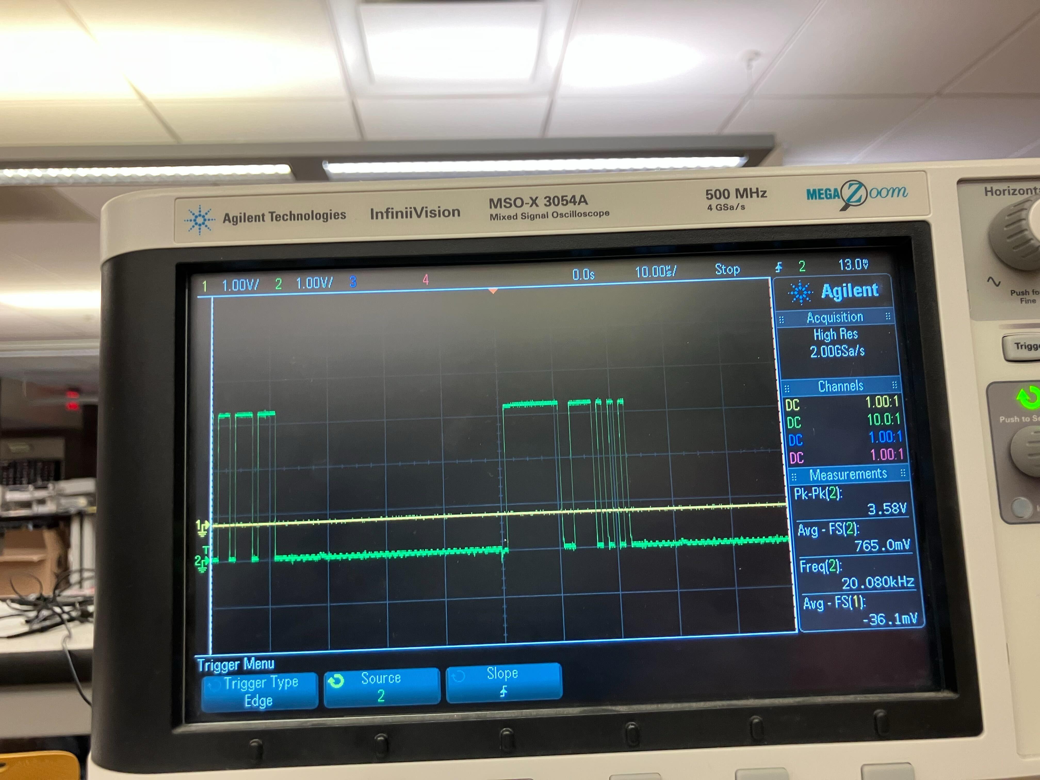
Digital output edges align to the clock for bit capture
Data toggles on defined edges enabling reliable sampling and decoding. This confirms synchronous serial behavior suitable for I²S/PDM-style acquisition.
IR Phototransistor: Analog output
We power the IR emitter, probe the phototransistor node, and observe analog voltage changes with illumination.
Probe across sense node and reference
Illumination modulates collector current, changing the sensed voltage across the load. This configuration establishes a clear baseline for assessing the light-dependent response.
IR diode power supply setup
IR diode powered on
The emitter is powered and positioned to control incident IR on the phototransistor for response testing. This enables repeatable stimulus while varying distance and angle.
Analog output changes with IR intensity
Increasing light increases conduction, lowering the sensed voltage across the load resistor. The transfer is monotonic within the tested range, enabling thresholding or analog filtering.
Individual Assignment: Input Device Measurement
Adding simple and complex input devices to a custom development board, successfully reading sensor data, and implementing edge AI inference.
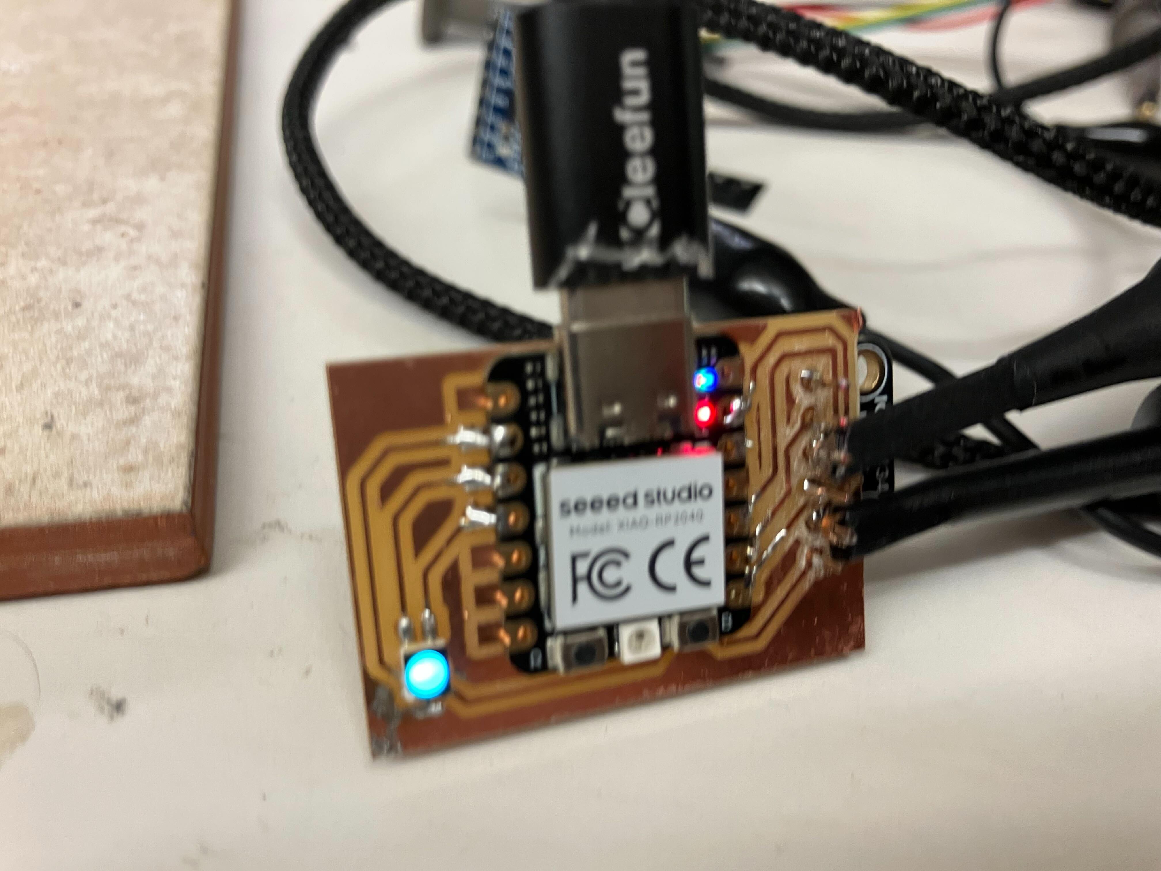
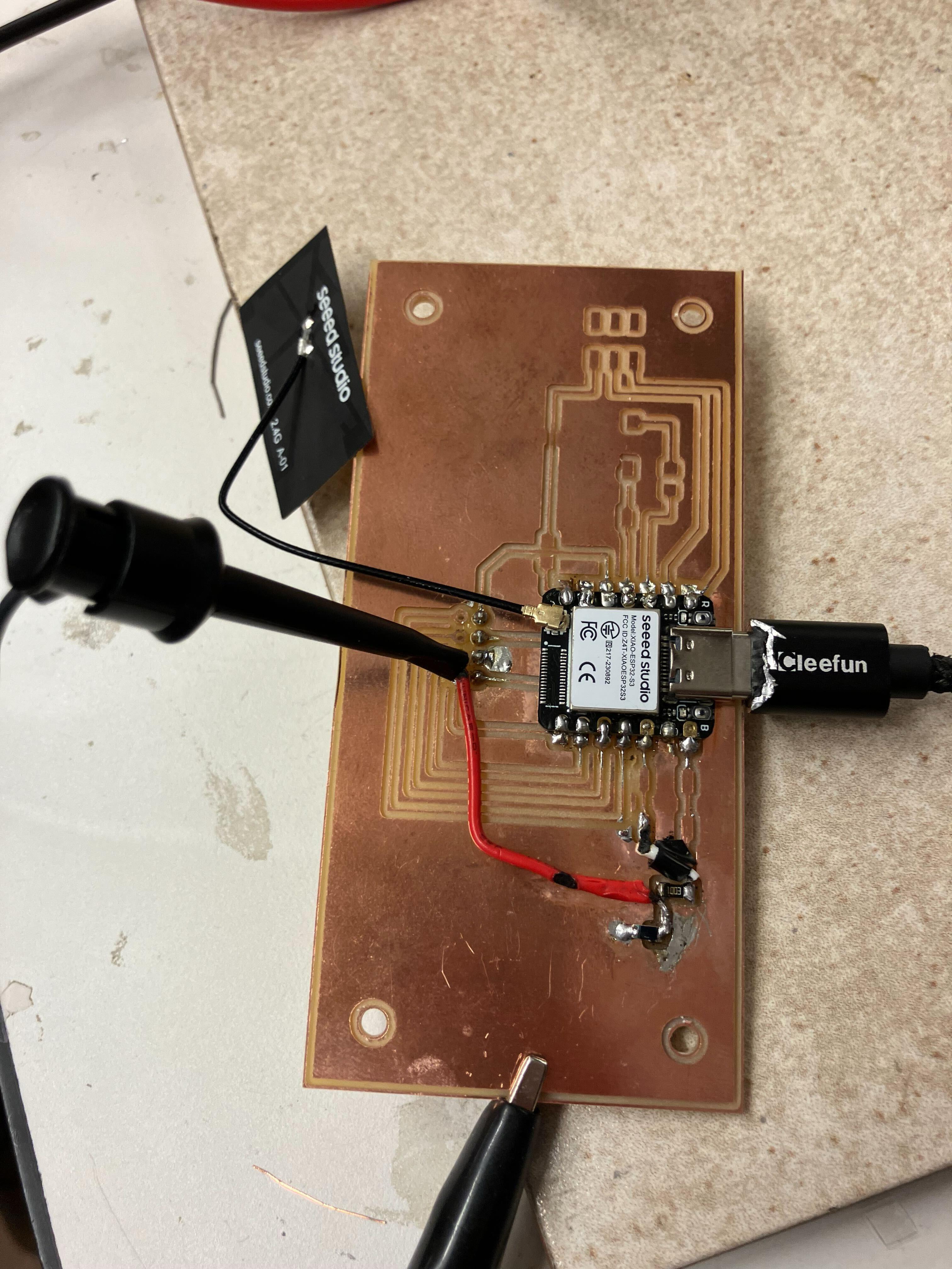
1. Remilling Development Board with ESP32S3
Using the development board designed in Week 4, I remilled the board to address an SDA/SCL short that prevented proper I²C communication for sensor visualization. The redesigned board incorporates an ESP32S3 with a presoldered camera module header in addition to the LED-button interface.
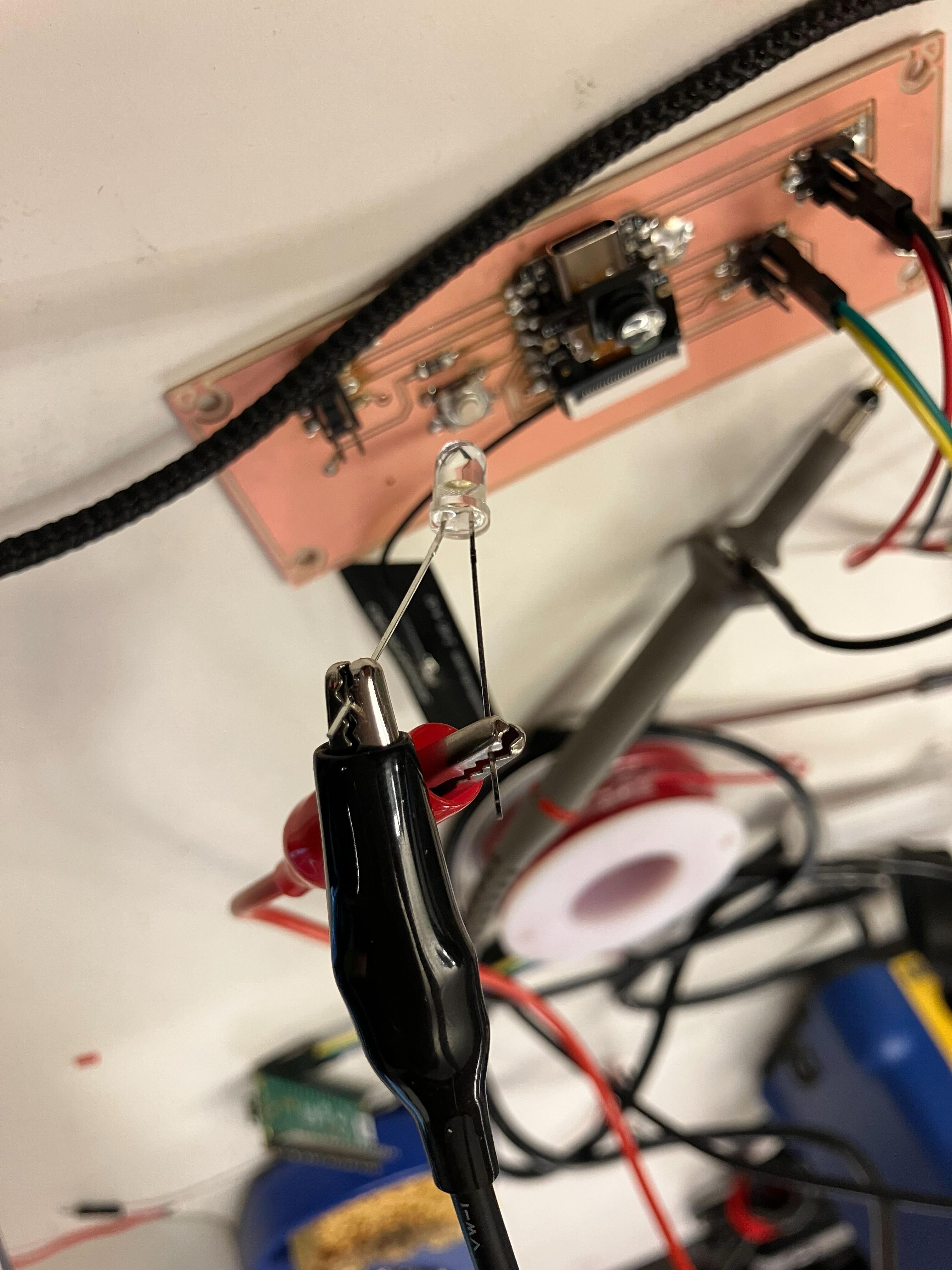
2. Simple Input Device: Button-LED System
Implementing the button-LED system using code from Week 5 to verify board functionality. The system provides immediate visual feedback confirming proper GPIO configuration and signal handling.
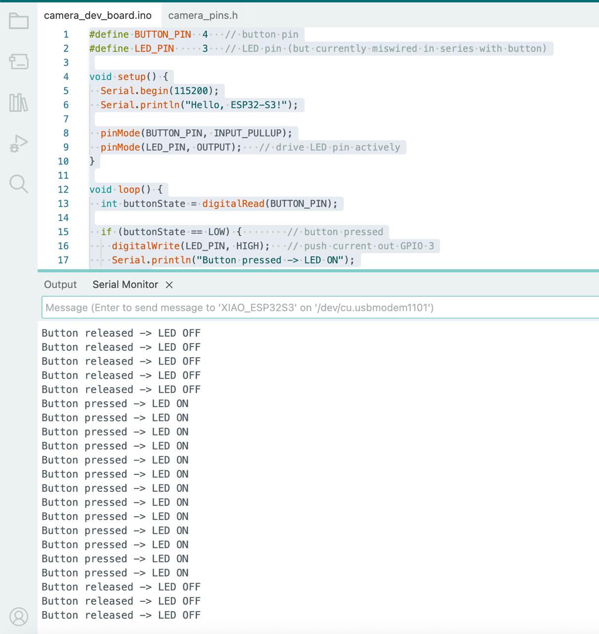
Button LED system successfully operational on custom development board
Button input device demonstration showing LED response to button press with real-time state changes
3. Complex Input Device: Camera with Edge AI Inference
Plugging in the camera module to the ESP32S3 requires careful soldering of a small pin header under the microcontroller using solder paste and hot air, so we purchased and used a pre-soldered ESP32S3 camera module to avoid issues with the header. The camera integration enables real-time image capture and edge AI inference on-device.
Edge AI Model Development
Developed an edge AI model using Edge Impulse with a dataset of ~60 training images and ~60 testing images. The model is publicly available at Edge Impulse Studio.
Workflow methodology based on embedded architectures recitation session by Erik Strand, covering camera integration, image preprocessing, and neural network inference on ESP32S3.
Implementation Results
Successfully captured images and obtained inference results via serial monitor. I²C display communication issues remain under investigation for the development board configuration.
Successful Output
18:42:41.622 -> Captured 160x120 (19200 bytes)
18:42:41.982 -> TTD: 12.103 years
Display Issue
18:42:41.622 -> E (158988) i2c.master:
  I2C transaction unexpected
  nack detected
18:42:41.622 -> E (158991) i2c.master:
  I2C transaction failed
While troubleshooting the display issue on the development board, I tested the camera inference system on the ESP32S3 camera subsystem from my final project, confirming successful edge AI inference functionality.
AI-Assisted Code Development
ChatGPT assisted in developing the camera inference code and troubleshooting the development board camera implementation.
Camera edge AI inference demonstration showing successful image capture and neural network inference on ESP32S3
Design Files
Complete design files for camera edge AI inference system including Edge Impulse library, Arduino firmware, and camera configuration.
Camera Inference Edge AI Model
The Edge Impulse library contains the complete inference engine for running neural network models on the ESP32S3. The library includes the Edge Impulse SDK with support for various sensor inputs, neural network inference execution, signal processing utilities, and classification output handling.
The model was trained on Edge Impulse with ~60 training images and ~60 testing images. You can view and interact with the model online at this Edge Impulse Studio link.
Camera Inference Microcontroller Script
The camera inference script captures images from the ESP32S3 camera module, processes them through the Edge AI model, and displays results on both the OLED screen and Serial Monitor.
How It Works (Pseudocode):
BEGIN Setup Initialize Serial communication Configure LED and OLED display Initialize camera module with grayscale format (160x120) Load Edge AI inference library END Setup BEGIN Loop Check for touch trigger OR 60-second timeout IF trigger detected THEN Turn LED ON to indicate capture Capture image frame from camera IF capture successful THEN // Display on OLED with dithering Scale image to 128x64 Apply contrast enhancement Apply Floyd-Steinberg dithering Display dithered image on OLED // Process for Edge AI inference Convert grayscale to RGB888 Prepare input buffer for neural network Run Edge Impulse classifier Get inference result (TTD value) // Display results Display TTD overlay on OLED Print TTD value to Serial Monitor ELSE Show error message on OLED ENDIF Turn LED OFF Return frame buffer to camera driver ENDIF Small delay (30ms) END LoopReflections & Learnings
Key insights and learnings from working with input devices and sensors.
Key Points
- Understanding sensor principles (load cells, microphones, IR phototransistors) enables appropriate selection for applications
- Signal conditioning and noise reduction are essential for accurate analog sensor readings
- Digital communication protocols (I2C, SPI) enable integration of complex sensors with microcontrollers
- Calibration is critical for converting raw sensor data into meaningful measurements
- Sensor fusion combines multiple inputs to create more robust and accurate sensing systems
Input Device Integration Insights
- Understanding the principles of various sensor types (load cells, microphones, IR phototransistors).
- Challenges in signal conditioning and noise reduction for analog inputs.
- Implementing digital communication protocols for complex sensors.
- The importance of calibration for accurate sensor readings.
Contributions
Acknowledgements and team roles for input devices work and references to related weeks.
Group AssignmentDone together by Saleem, Mariam, Jyo, Guillermo, Alex, Jessica, Aijia, and of course, Anthony!
Camera Display ReferenceCamera display and Edge AI inference demonstrated in the final project camera subsystem. View camera subsystem
Input LED ReferenceButton-LED implementation documented earlier in Week 5. View Week 5 individual assignment
Ethical AI Use
Transparent documentation of AI assistance used in this week's input devices work.
📋 General Guidelines: See General Commands for Cursor on the homepage for standard guidelines and commands used consistently throughout documentation development.
AI-Assisted Week 7 Page Creation and Group Assignment Documentation
Cursor AI assisted with structuring this page, refining the group assignment documentation, creating the two-row highlights, and polishing the individual assignment text. The transcript below captures the session focused on Week 7 updates and guidelines.
AI-Assisted Camera Code Development
ChatGPT assisted in developing the camera inference code and troubleshooting the development board camera implementation. The AI provided guidance on camera module initialization, image capture optimization, Edge AI model integration, and I²C display communication debugging.
 This work is licensed under a
Creative Commons Attribution-NonCommercial-ShareAlike 4.0 International License
This work is licensed under a
Creative Commons Attribution-NonCommercial-ShareAlike 4.0 International License