
Aijia Yao
Week 14 – Wildcard Week: Microfabrication
December 2025
This week was mainly about microfabrication.
What I Did
- Designing patterns for direct-write photolithography on 4" and 6" wafer.
- Using web scraper to collect HTMAA+Fab Academy names and python phidl package to create gds file.
- Fabricating the 4" wafer with lift-off process and the 6" wafer with etch-based process.
Why Microfabrication?
The inspiration of this week came from One.MIT project which collected and shaped all the names of people from MIT into mosaic patterns and then "printed" on Si wafers with photolithogrphy. On these wafers, each name is tiny—almost too small to notice on its own—but collectively they build a structure that carries identity, history, and community. Microfabrication works the same way. It is the discipline where the smallest features, patterns, and layers define the performance of entire systems: devices, circuits, and technologies that shape how we live.
Since most of my PhD research has been struggling with nanofabrication, which is mostly done with electron beam lithography(EBL), this week I decided to try out the happy world of microfabrication based on photolithogrphy with two kinds of process flows: lift-off and etch-based.
Lift-off Process
Using fabublox, I can easily pull up templates to demonstrate the process flow using photolithogrphy as in the following diagram:
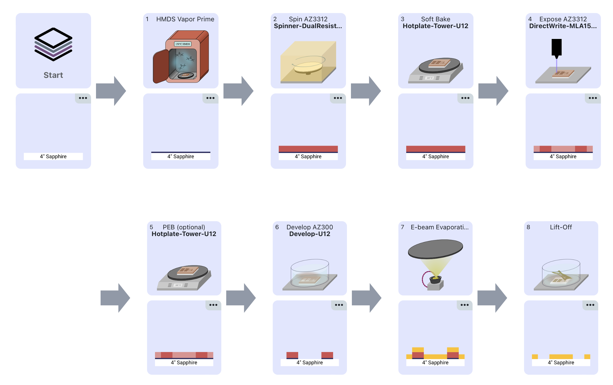
For lift-off process, the photoresist is patterned to create openings only in the areas where the final material layer is desired; all other regions remain covered by resist so that deposited material on top of the resist can be removed during lift-off.
Etch-based Process
If you ever pass by the front door of MIT.nano, you will see a gallary of wafers with images patterned from the MIT.nano IAP course, their shiny blue color comes from sillicon nitride(SiNx) deposited on sillicon(Si) wafer and the silver/grating patterns are aluminum(Al). Below is the process flow showing how to fabricate these wafers:
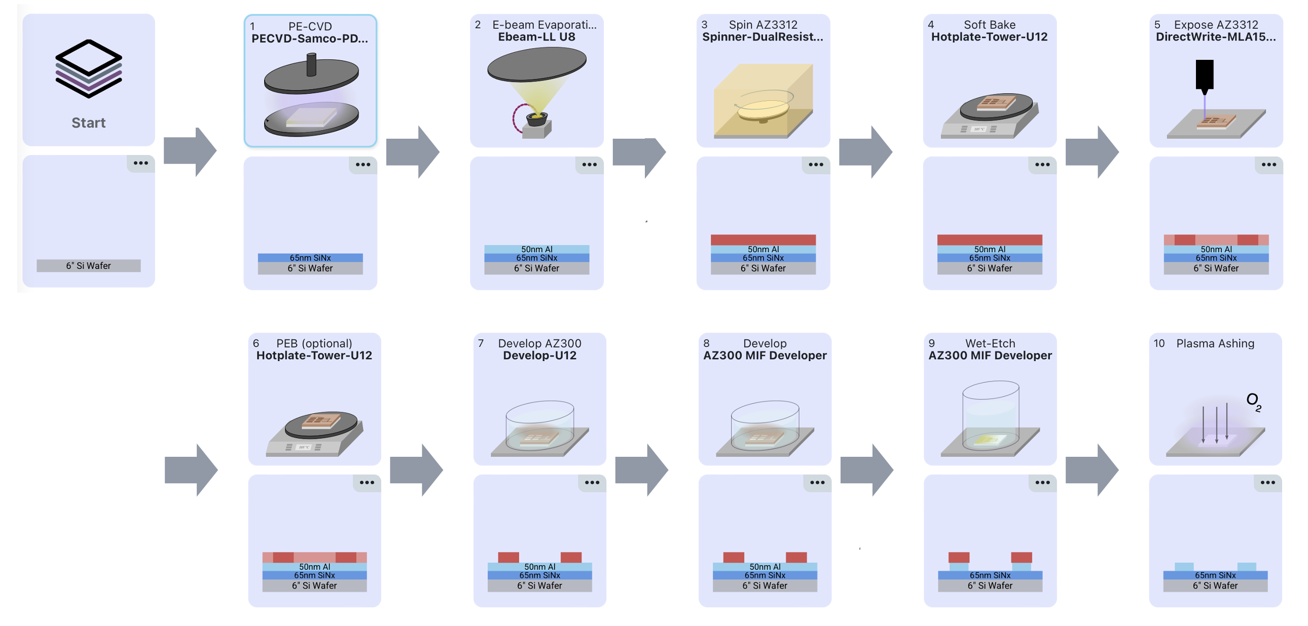
For etch-based process, the photoresist is patterned to to act as the etch mask, selectively shielding the underlying material so that only the exposed regions are removed during etching. This process was developed and shared by Dr.Jorg Scholvin, Associate Director of FAB.nano. The nifty trick in this process is that the developer for the photoresist, AZ300 MIF, has a main component called tetramethylammonium hydroxide (TMAH), which can etch aluminum by dissolving its native oxide layer and forming soluble aluminate complexes. Hence, step 8 and 9 can actually be done in one step by simply extending the time of the sample soaking in the developer to first dissolve the exposed area and then etch away the aluminum in the openings.
Pattern Design
Following the idea of putting names into mosaic pattern, I inquired Jorg on the algorithm they used for One.MIT. Based on his feedback, I realized the "kerning" method used in One.MIT requires complicated parameter optimization because the bold letters change the spacing between words and without a huge number of names as the buidling block, this patterning method may end up having "choppy" results.
Collecting Names
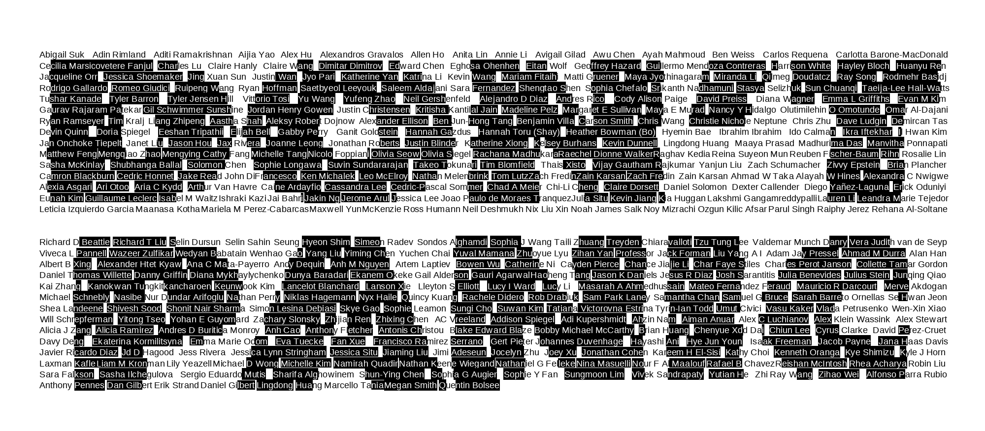
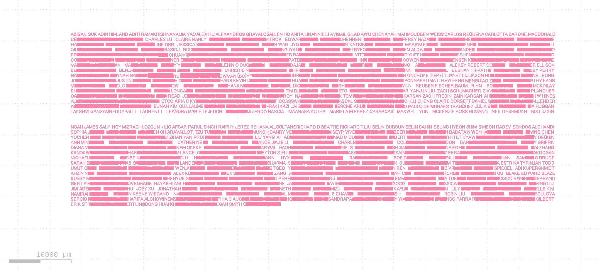
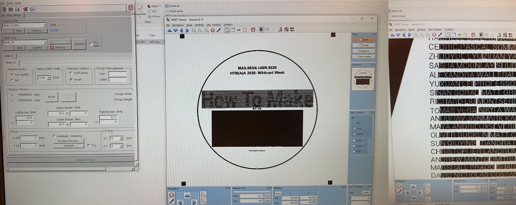
To estimate how many names will be used in this pattern, I wrote a scraper to parse through the "people" page of all the HTMAA website. Though I found many links have been eroded by time online, I still manage to pull down the full name list from 2008-2025 including all the students, TA, instrauctors, Gurus, etc. For names between 1998-2007, I just then manually collected them from different corners of the web. I also found the alumni name list for Fab Academy so collecting the names from this page is much easier. For HTMAA people, you can search your name here in the raw data. And by searching you may find some interesting coincidence of same names and same person/people repeatedly showing up in different years. To make the final version cleaner, I just kept one name in its latest occurence, e.g. Prof. Neil Gershenfeld's name would be only showing up once in 2025. After removing dubplicated names and adding 1730+ people from Fab Academy, it rounds up to ~3k names in total, this number will later be useful when coverting gds file.
Patterning Text
Then, I wrote up my own code with help of ChatGPT 5.1 [see prompts here], and instead of applying a bold font, I inverted its pattern so that the background provides the visual contrast. To speed up the debugging process, I started a test run with only names from 2020-2025 and try to pattern them to show the message "Don't Panic"(which is a phrase on the cover of The Hitchhiker's Guide to the Galaxy [reference link]).
The workflow for this patterning is simple: arrange the names in rows to cover the entire shape, then invert the text wherever the underlying pattern exceeds a chosen darkness threshold. The test worked well as shown above, the code for this part is also included in the jupter notebook you can find in 'Other Notes'.
Converting To GDS Layout
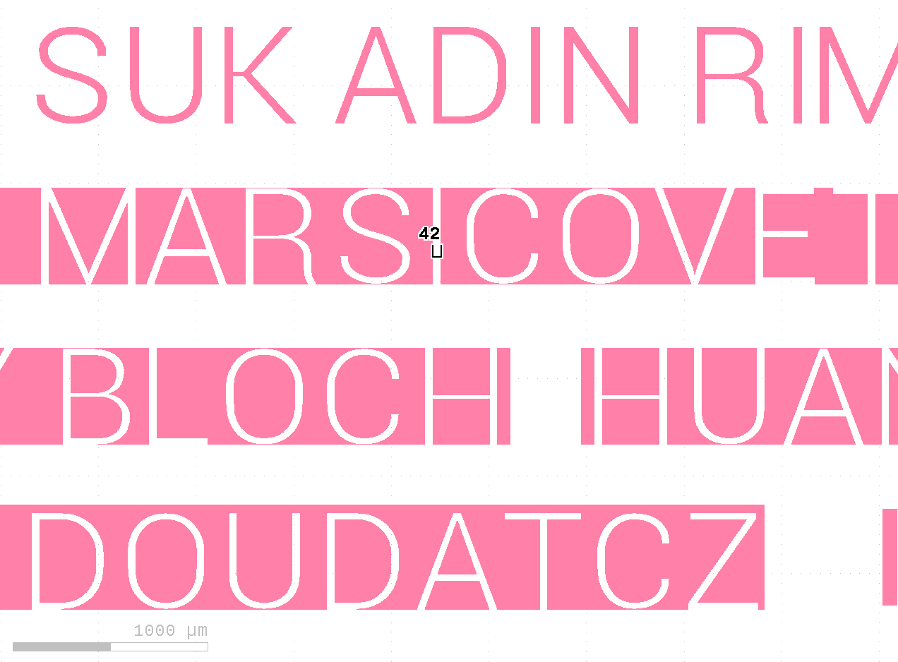
With the "inverting" part working, I then used phidl, an open-source Python GDS (GDSII) layout and CAD geometry creation tool to put the pattern into gds layout, which is the file format for direct-write lithography input. And this time I found, because the text are treated as shape/polygon in gds, the alignment of the letters became messy if both upper and lower case are put together.
 |
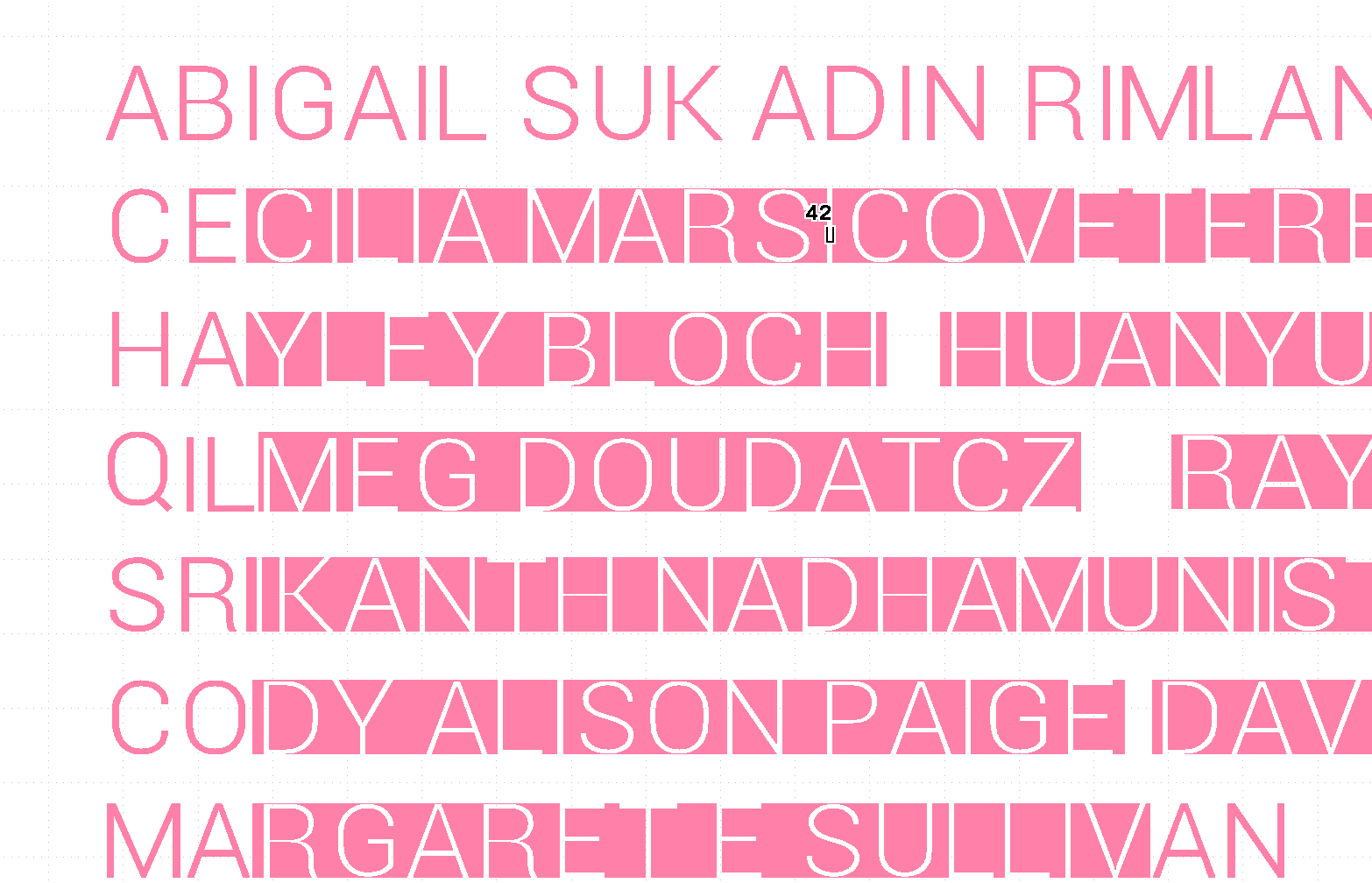 |
So, for the best visualization of a big chuck of words, I just keep everything uppercase. And with fine-tuning of the text font, text size and pixel width conversion(in micrometer), the layout can be made quickly and beautifully with each pixel converted to 42um in layout.
|
|
A Hitchhiking Test Batch
For the test run, since i had reached this far patterning names between 2020-2025, I just decided to add names from 2019 and continue to test next part of the design with a golden rule called "Just Ask Anthony":)
 |

|
To convert the image shown on the left to the diffraction grating pattern shown on the right (check the scale bar at the corner and the measure unit is um), I used the python code developed by Dr.Jorg Scholvin (see Github repo here). Then combining both the names patterned as 'Don't Panic' and the grating patterns, the final gds file was made. Since I already had a metal evaporation step scheduled for my own research samples, I quickly fabricated the patterns so they could catch the same run—essentially hitchhiking. Fabrication notes for this batch are as follows:
Substrate Preparation
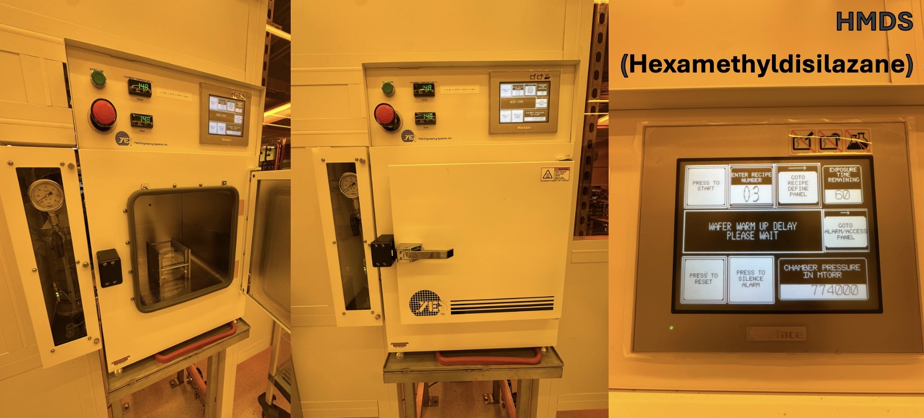
Starting with 4-inch double-side polished sapphire substrate, the first step is to apply HMDS (hexamethyldisilazane) to dehydrated wafers, which is one common method for achieving the surface hydrophobicity required to prevent photoresist delamination [ref1, ref2].
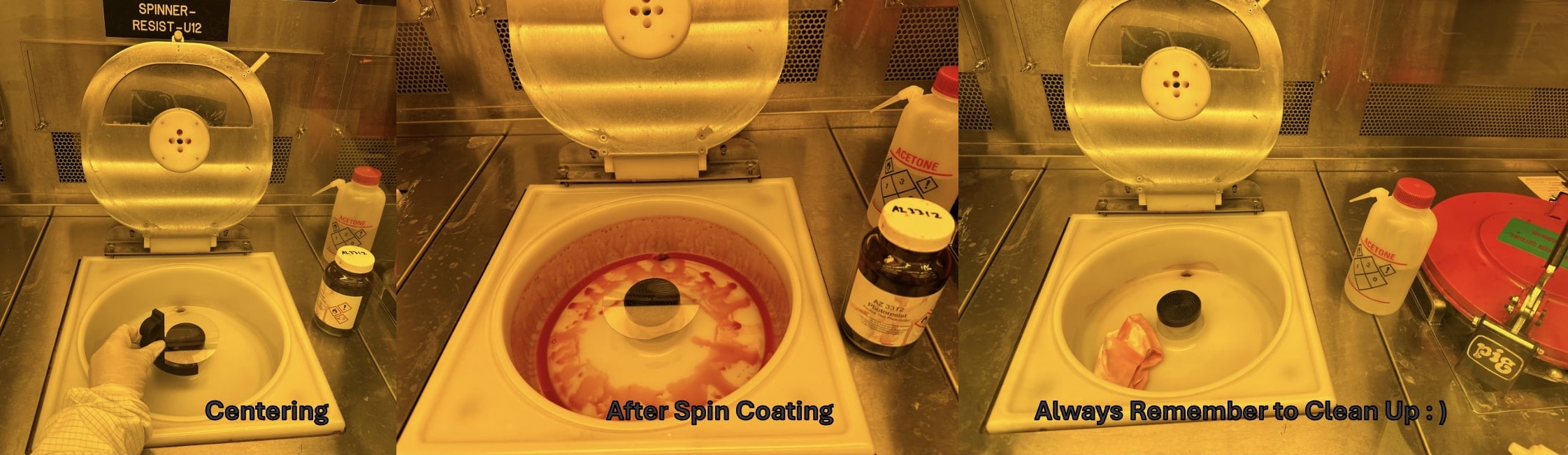
Next, AZ3312 photoresist was spincoated on the wafer with 3000 rpm for 60s on spinner, followed by 90°C baking for 100s. Though it's not easy to see since I'm using an almost transparent wafer, it is important to align the wafer to the center of the spinner with the help of the aligner shown in the left image. And using acetone and fab wipes, the messy photoresist can be cleaned.
As you may have noticed, all of the steps above were carried out in a yellow-light zone to minimize photoresist exposure and ensure pattern fidelity throughout the process.
Exposure with MLA150
Since I was in a rush to catch the hitchhiking run, not too much details were noted here, so definitely check the exposure notes for the 6-inch wafter for more info. The tool I used for direct-write photolithography is MLA150, and below is a recording of its UI showing the estimated exposure time and the screen on the right is showing its microscope view.
Developing
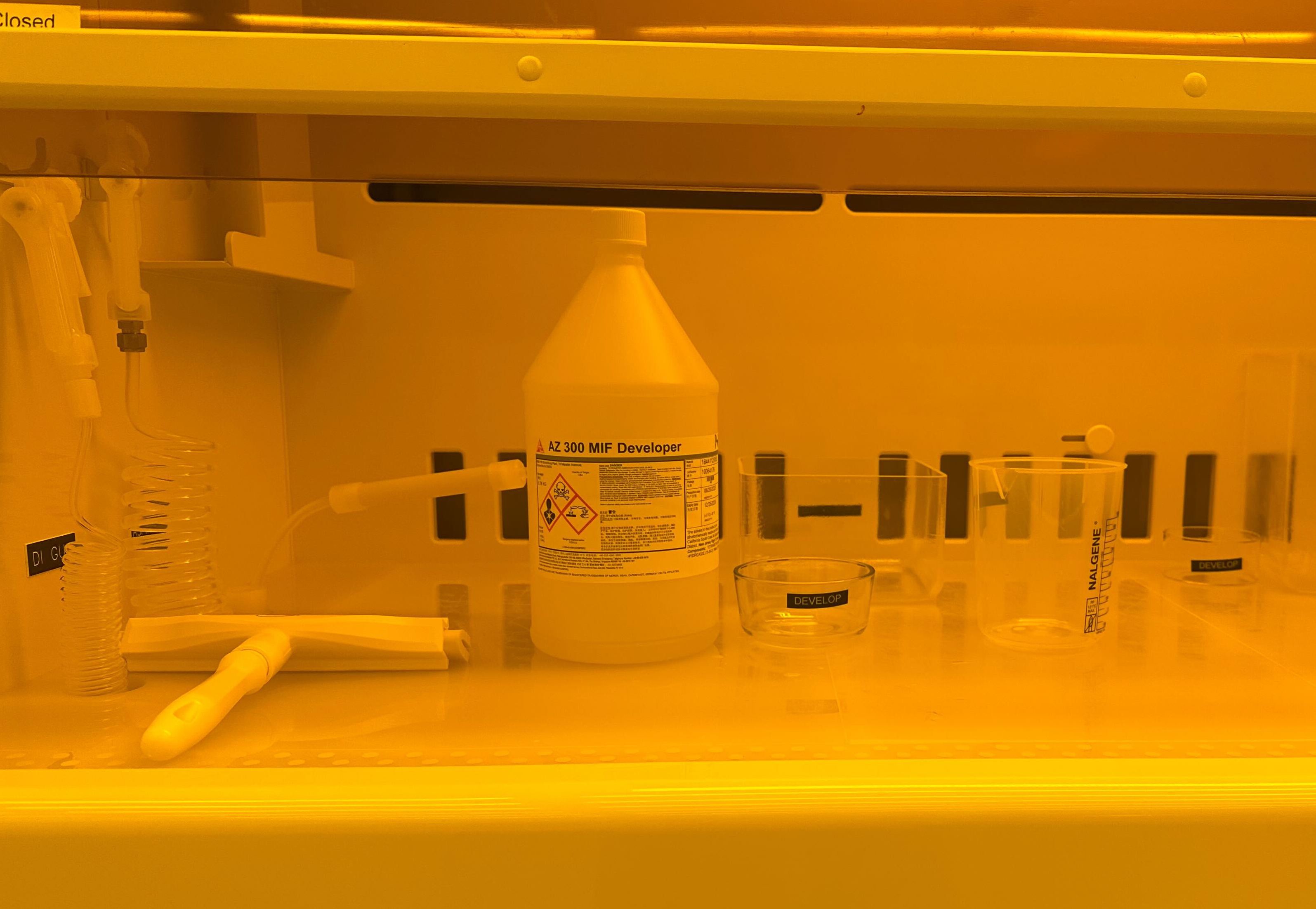
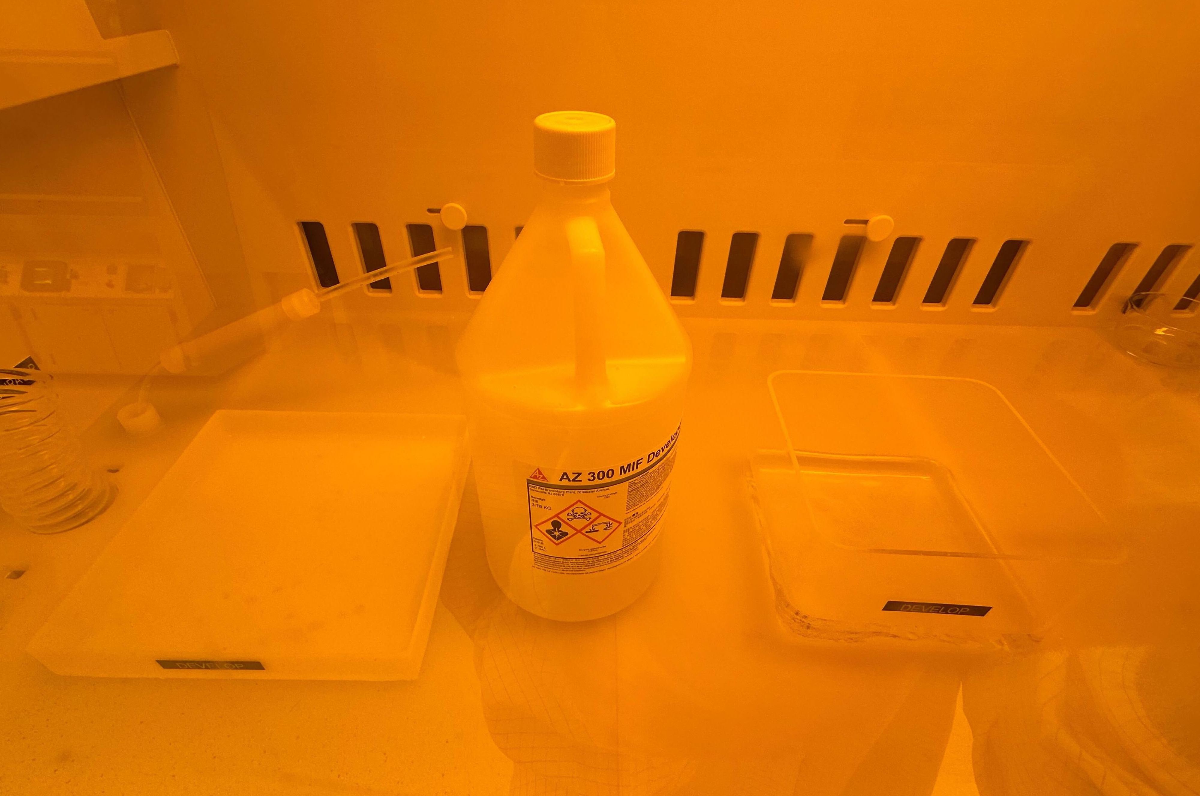
After the exposure, I baked the wafer at 110°C on the hotplate for 100s (this step is optional based on different process design) and then proceeded to develop it in AZ300 MIF developer for 70s, after that, rinse with DI water[must operate in a developing fume hood].
 |
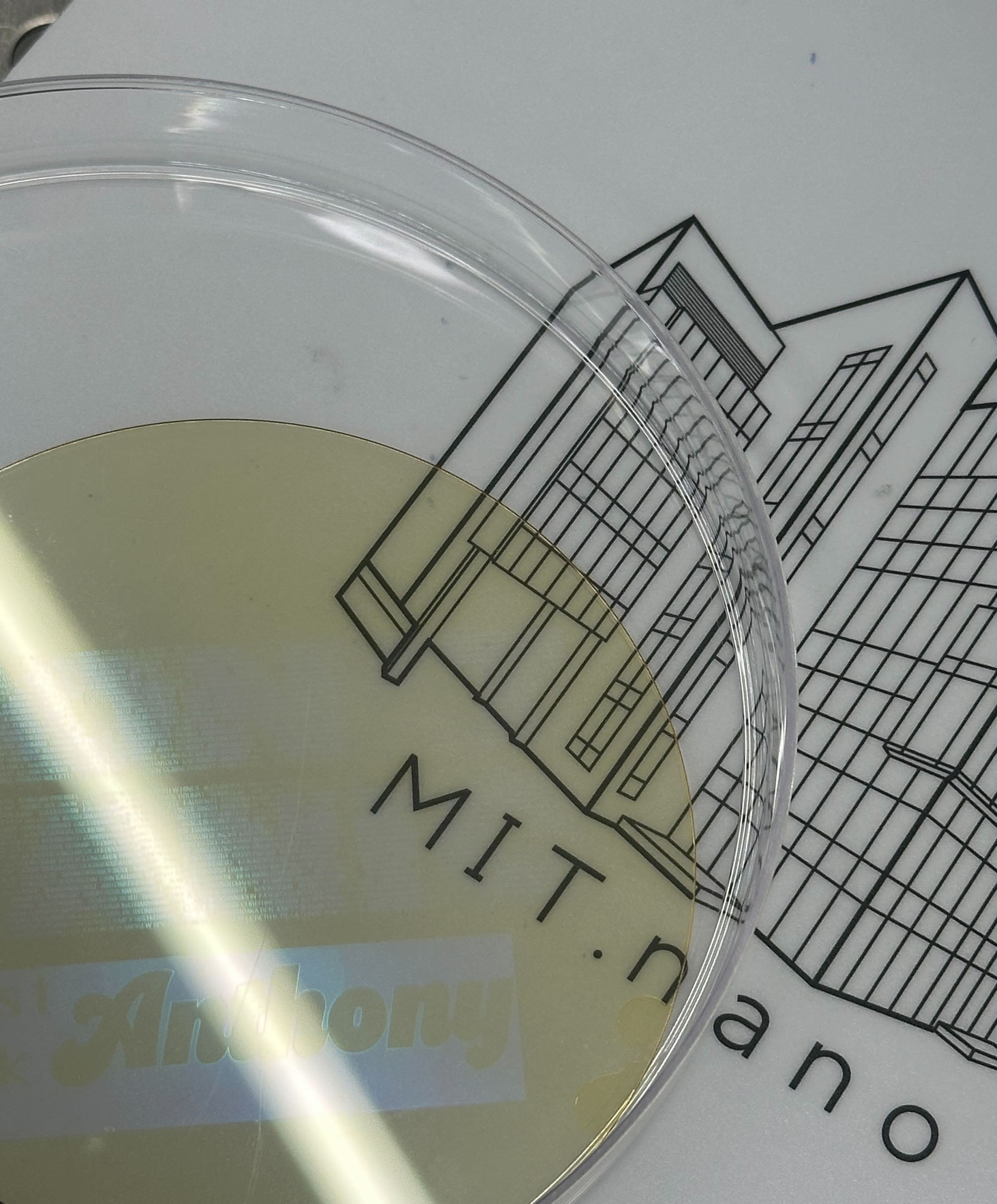 |
Since the exposed photoresist has been removed after developing, the pattern on the wafer can be seen as shown in the image on the right.
Metal Evaporation and Lift-off
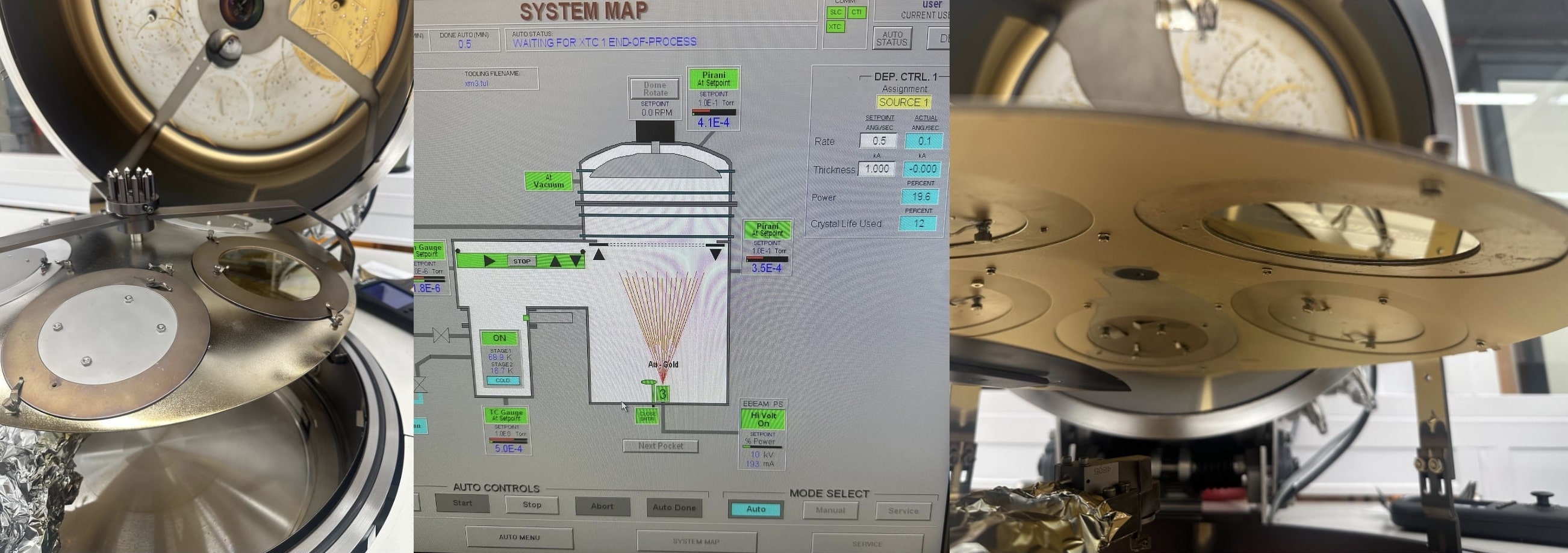
Till this step, the pattern has been defined by the photoresist on the wafer. I used electron-beam evaporation tool to deposit Ti/Au 5/100nm on the wafer as shown below (respectively before, in progress and after the ebeam evaporation).
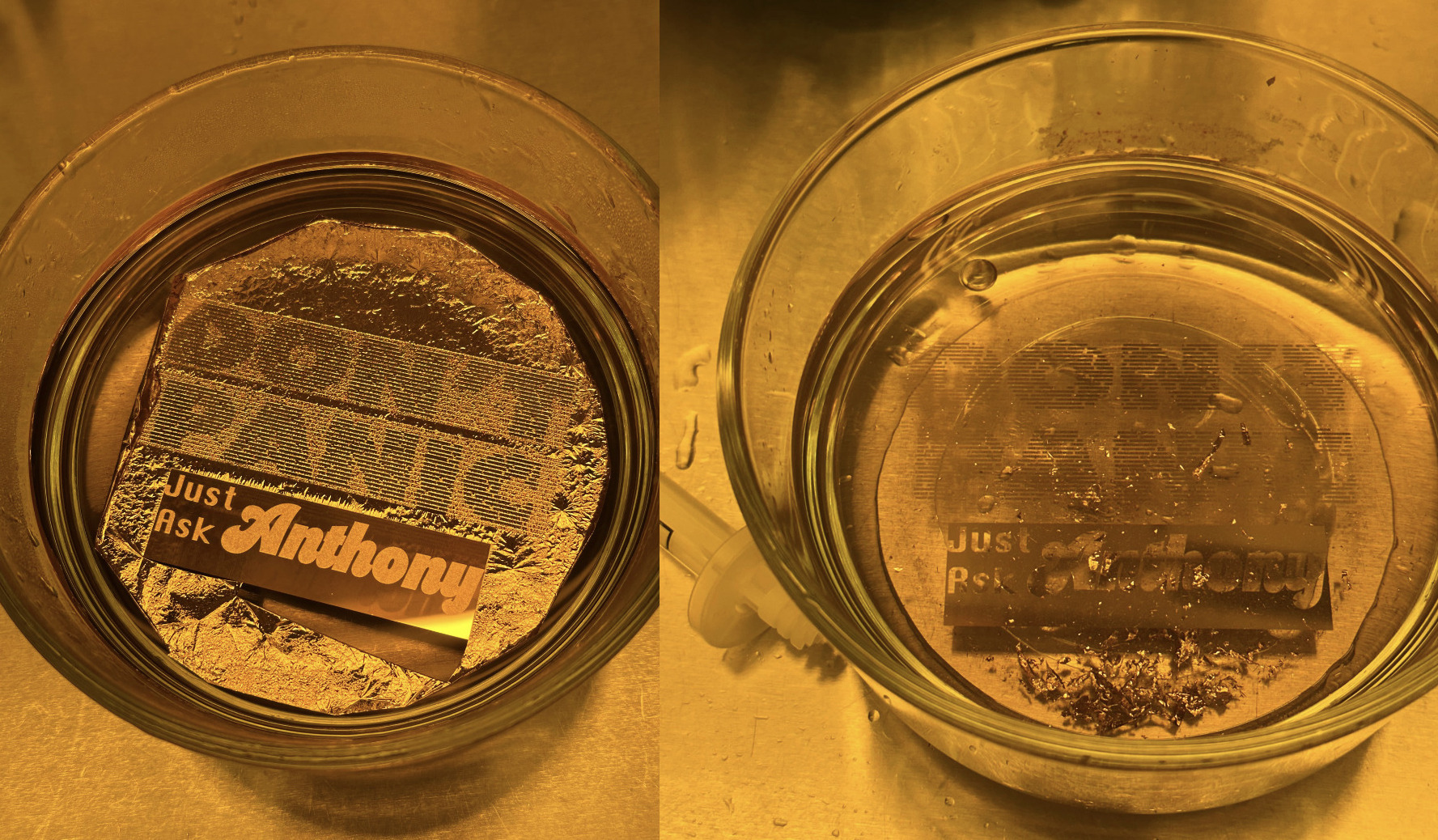
Finally, to remove the photoresist and lift off the excess metal, the sample was soaked in N-Methyl-2-pyrrolidone (NMP) solvent in a 70 °C hot water bath. The picture on the left below is the sample after 20 mins NMP soak, the edge started to peeling off but most of the metal are still on the sample. The picture on the right is the final lift-off result after soaking for a few hours.
"HTM(A)A" Wafer
With experience gained from the test batch, I continued to design and fabricate the 6-inch wafer with etch-based process.
Pattern Design
One lesson I learned from the test batch is the importance of keeping both the text patterns and the diffraction grating patterns properly scaled to achieve a consistent appearance and accurate dimensions. So before I add anything specific, I drew a sketch for the wafer design:
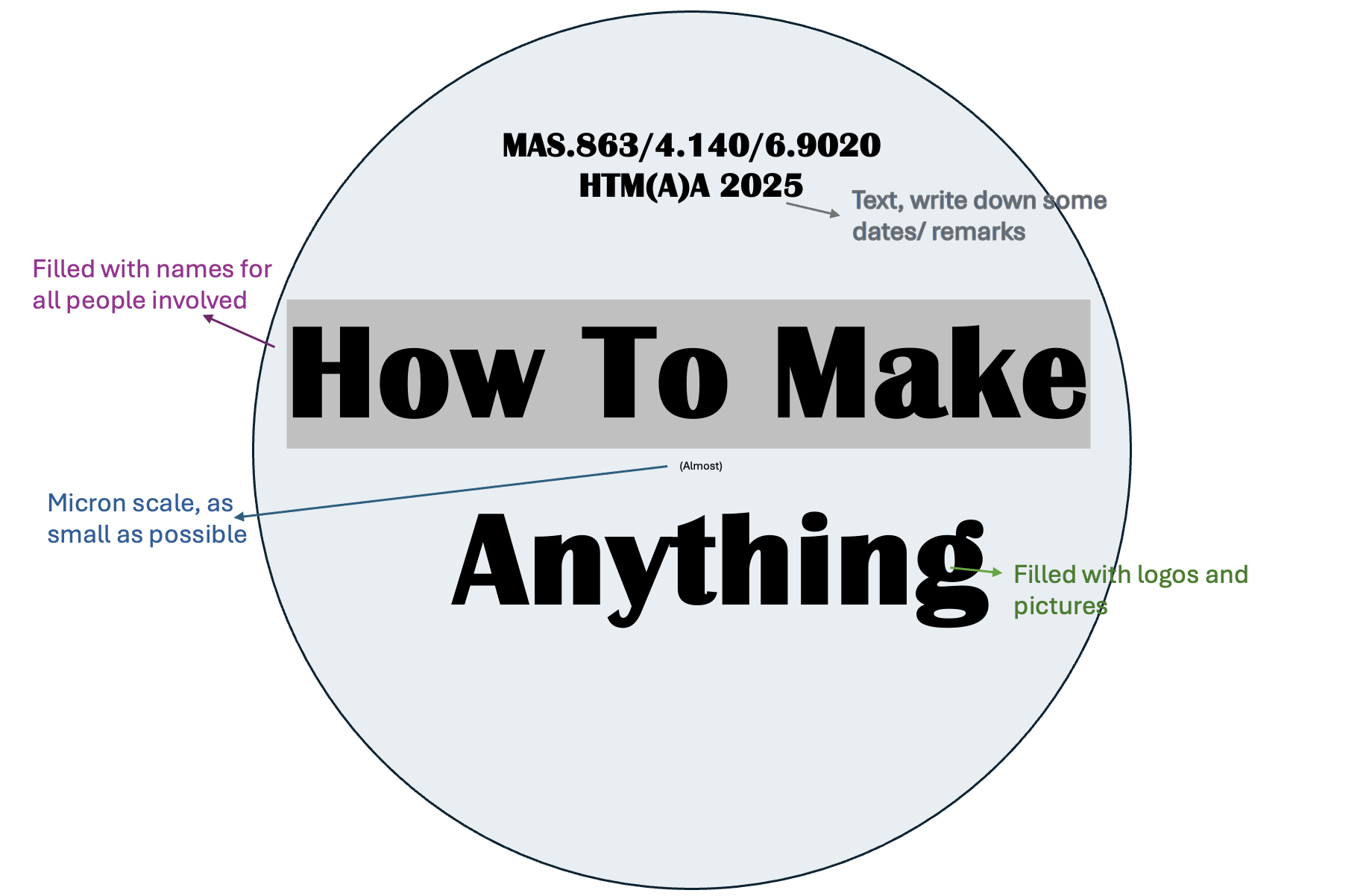
After brainstorming+organizing the elements (logos and fonts) needed for the design, I put them all on the same canvas using Adobe Illustrator as shown in the figure below:

The background image I used is The Pillars of Creation from NASA’s James Webb Space Telescope’s near-infrared-light view. For best fabrication result, this image should be rich in pixel detail. Hence, an ideal choice being astronomical images of nebulae, which offer exceptional resolution and intricate structure, and the name 'Pillars of Creation' also matches the theme here. After placing all the logos related to HTMAA, I found that there was still plenty of unused space, so I used the PCB traces from our class page to fill in the letters “hi”, together with Fab Academy logo, the “hi” motif stands as a tribute to the classic “hello, world".
Substrate Preparation
For etch-based process, the metal was deposited before the photolithography. And to give the wafer a bit of color, 65nm sillicon nitride (SiNx) was deposited with PECVD to make the Si wafer shiny blue. Many thanks to my labmate Leo who was depositing SiNx with the PECVD tool for gate dielectric and gladly used this 6-inch Si wafer as rate calibration test.
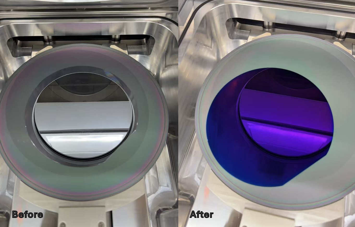
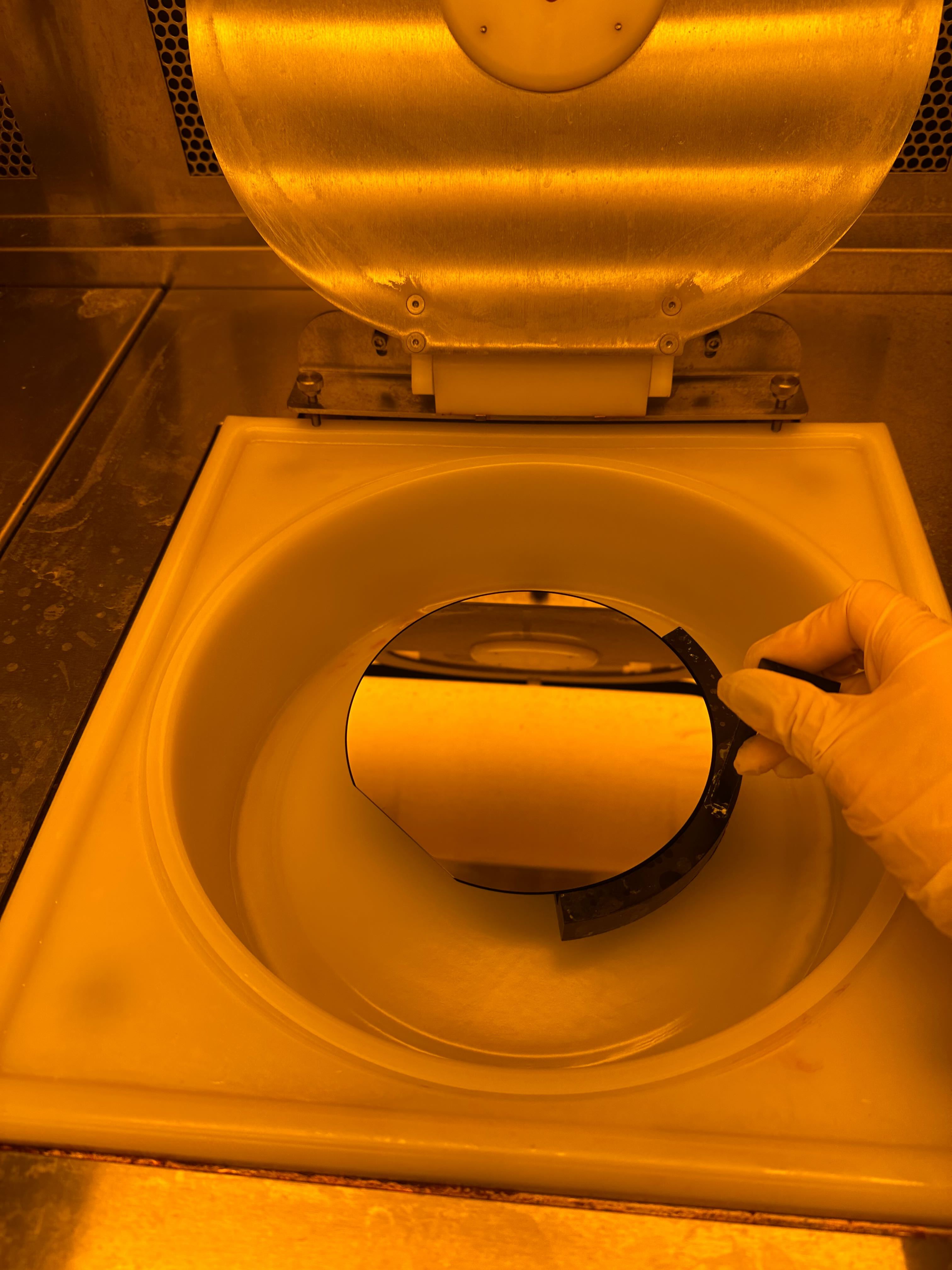
After PECVD, e-beam evaporation was used again to deposit a 50 nm aluminum layer on top of the SiNx, forming the silver strokes retained after etching. Next, a layer of photoresist AZ3312 was spin-coated onto the sample to prepare it for photolithography. The resist was dispensed onto the wafer and spun at a controlled speed(3k rpm for 60s) to achieve a uniform thickness across the surface, notice again to make sure the wafer was centered using the aligner as shown in the left image below. Following spin coating, a soft bake at 90°C for 100s would remove excess solvent and improve resist adhesion before exposure.
 |
Exposure with MLA150
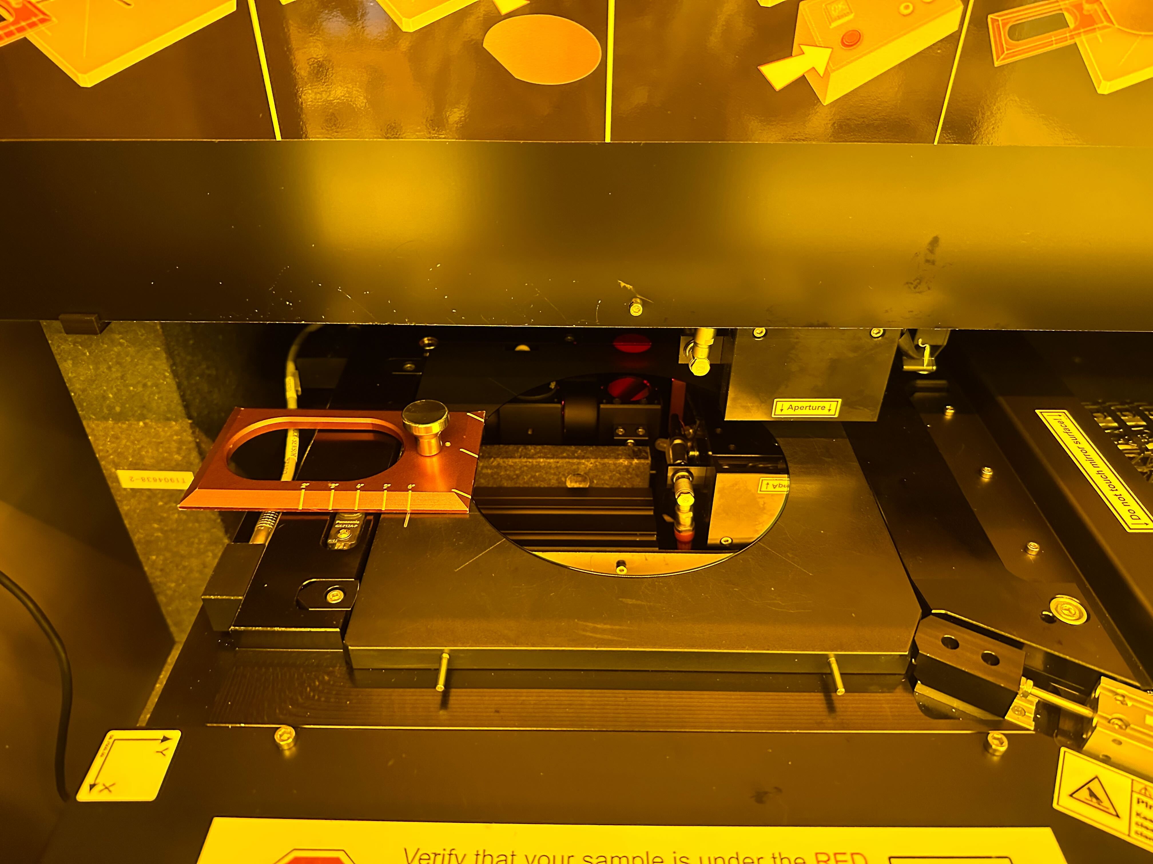
Different from the test batch, although it's still MLA150, since the wafer is 6-inch, I switched to the wafer-only MLA and used the wafer aligner as shown below. (⚠️ MUST REMOVE ALIGNER BEFORE LOADING FOR EXPOSURE⚠️ otherwise it will stuck between the holder and the laser)
One thing very critical here is that make sure to INVERT the pattern in the exposure setup. Because this is an etch-based process, whatever exposed will be later etched away. So make sure the "invert" was ticked since the viewer only shows the gds layout, not the inverted view.
Developing and Etching
This time I did't do post-exposure baking and directly started developing in AZ300 MIF developer. Notice: ⚠️TMAH (tetramethylammonium hydroxide), the active component in AZ 300 MIF developer, is a highly alkaline and acutely toxic chemical that can be absorbed through the skin. Due to these safety concerns, the developer must be handled with appropriate wet-bench precautions and nitrile gloves to minimize the risk of exposure.
|
In the video above, the etching started to show the contrast at around 50s, which was about 2 mins after soaking in AZ300.
Cleaning Up
After removing the wafer from the developer and rinsing it with DI water, the patterns appeared very clear, as shown in the left image below. However, unexposed photoresist remained on the wafer, so an additional oxygen plasma cleaning step was required to ash the resist.
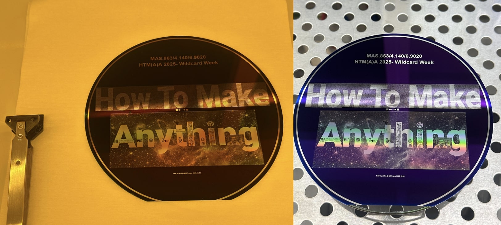
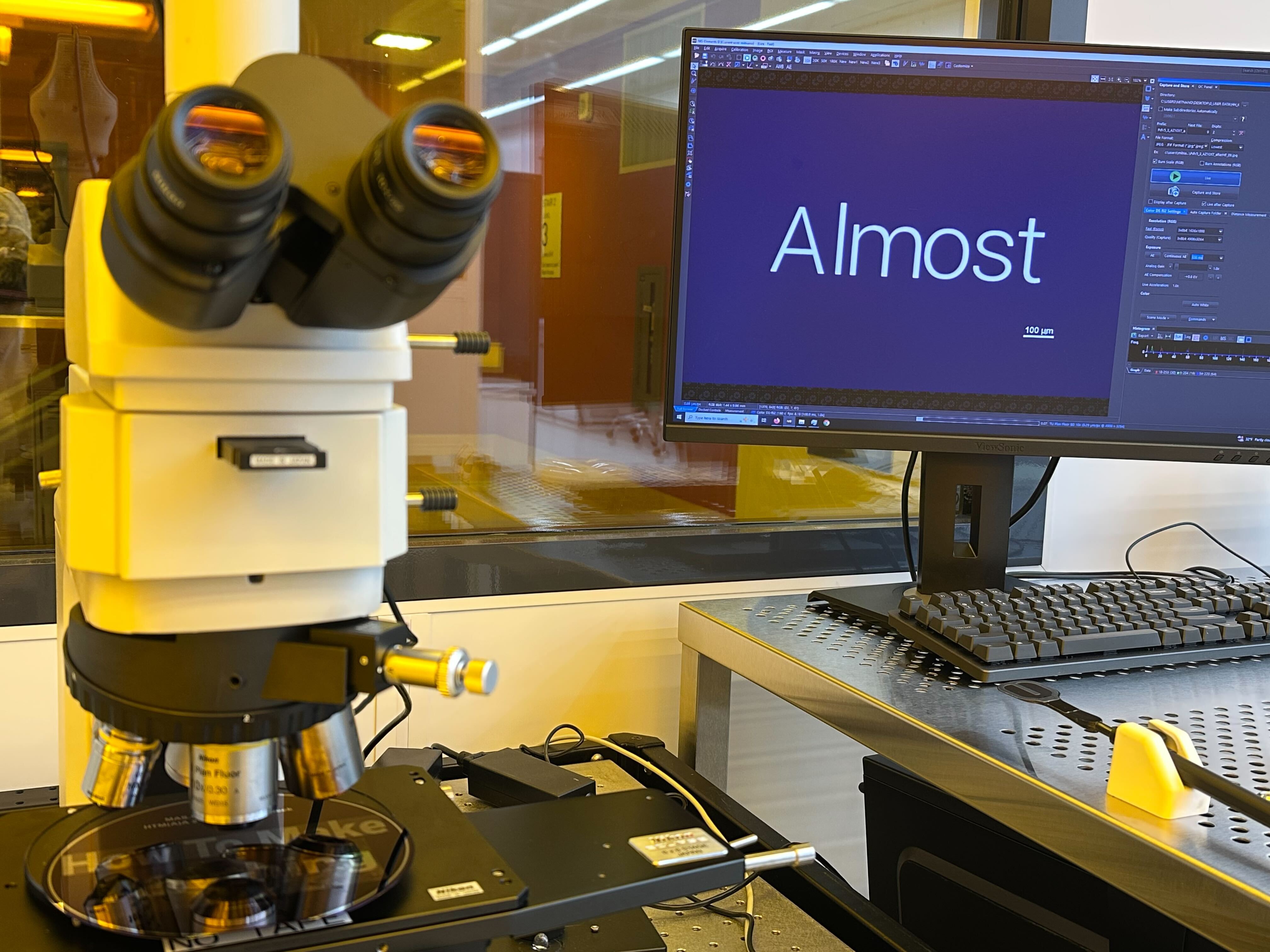
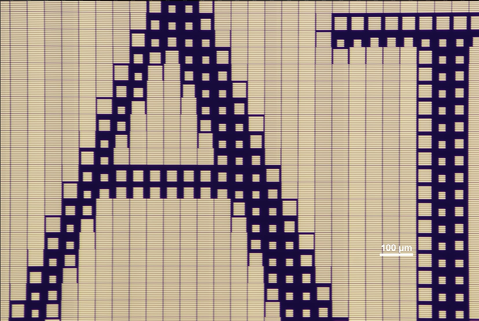
The final plasma-cleaned wafer is shown above on the right. Under the microscope, the word “Almost” appeared so clearly that it looked more like a displayed text on an image than a microscope view.
For the diffraction grating pattern, here is what you can see for "AT" in "CBA"'s "ATOMS" under the microscope:
Other Notes
- Two wafers succeeded in the first fabrication trial really makes me happy🥳 since it's not always the case for nanofabrication🥲.
- Since I had very limited time for design and fabrication, the names on the wafer may contain duplicates, typographical errors, or omissions. Please forgive any imperfections in this batch; after all, to borrow Richard Feynman’s reminder, “There is plenty of room at the bottom.”
- Use this dropbox link for the python code and gds files used in this wildcard week.