Week 6: Electronics Production
Assignment
- group assignment:
- characterize the design rules for your in-house PCB production process
- submit a PCB design to a board house
- individual assignment:
- make and test an embedded microcontroller system that you designed
Group Assignment
Please see this link (Session 3) for my group's assignment.

Website Update
As you may have noticed, this sub-page has a different look to it! During last week's presentations, I was inspired by Sara Ferandez's website. Its clean design and straightforward user interface was exactly the kind of aesthetic I've been looking for. I asked to meet up with Sara and she was kind enough to show me her method for documentation. This week, I am trying out her method. Thanks again Sarah for the tips and tricks!
Individual Assignment
Last week, we designed and simulated a PCB. I decided to design a board which demonstrated three different types of low pass filters. Although it was passing all of the design rules by the end of last week, there were a number of practical considerations that I needed to take into account. See below for what my layout looked like at the end of last week.
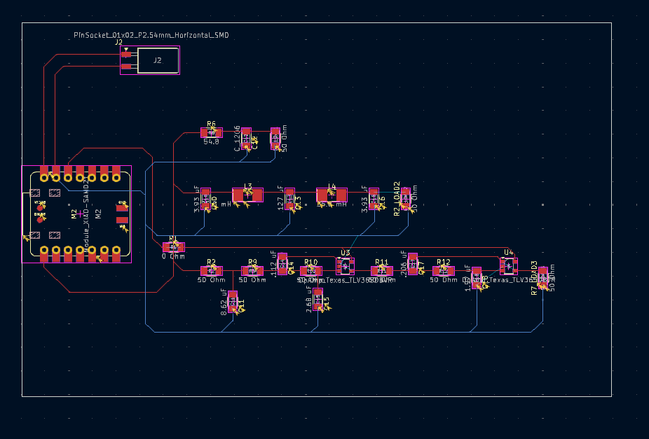
Thanks to recitation, a really helpful design review session with Dimitar, insights from Matti and Miranda, chattng with Anthony after class, and many more hours of refinement than anticipated, I ended up with a board that looked something like this.
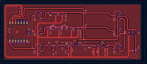
Things I changed to improve manufacturability:
- Turned this into a single sided board
- Increased track widths
- Inclusion of a back pour
- Addition of an op amp at the end of my signal paths
- Utilization of switches to open and close the different signal paths
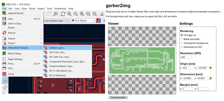
Next, I started working through the process of making my design come to life, using the Carvera Mill in the CBA electronics shop. I followed the instructions on Quentin's Carvera PCB Tutorial. Huge shout out to Quentin for this amazing document!
Step 1: Convert from PCB to Gerber to img
Use Quentin's gerber2img tool in order to convert the fabrication files exported from KiCAD (gerber files) to two color images. You need to make one for the edge cuts and one for the traces.
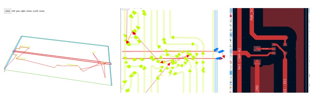
Step 2: Generate G Code
Next, I used the "Carvera Mill 2D PCB Program" which is hosted on https://modsproject.org/ to convert these images to GCode. Quentin provides directions for how to open and use the Carvera program in his tutorial. When I opened up the output, I could tell something was wrong because there were far fewer tracks than I expected (below left). A classmate helpfully pointed out that you need to make sure to check the "Black and white" rendering option on the gerber2img program. When I tried to export again, there were many more milling paths, but they weren't cutting my smallest traces (below middle). Those small traces are associated with the Op Amps in my circuit (below right). Turns out, that I had the board constraints in KiCAD improperly configured. My minimum clearance was 0.1 mils but needed to be 0.4 mils given the Carvera's tolrance. So, although my board was passing the ERC, it was improperly configured, which is why I didn't catch this issue earlier in the process.
Next, I spent quite a bit of time re-working my traces in order to accommodate for the 0.4 mils clearance (see below). Fortunately, I had the pleasure of being around many of my fellow cba section classmates down in the electronics lab, which made this re-work much more enjoyable.
While I worked on this re-design, I couldn't help but notice that all the folks who had milled fine traces were no struggling to populate and debug their boards. I had a feeling that even though my board was now passing the updated design rules, that I too would struggle with populating more board if I went through with milling it.
It was a hard choice to make, because I was really eager to see this board through, but I'm trying to do a better job of "spiral development" and "supply side time management".
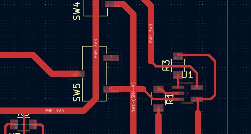
So. The next day, I opened up a brand new KiCAD project and got to work making a much simpler design: a board with a single passive RC filter using a potentiometer for the resistor so that I could dynamically alter the cutoff frequency. Functionally, this would also be cool and enable me to demonstrate a variety of low pass filters, but I would be able to use far fewer component and stick to bigger traces.
Step 3: (redesign) and use Carvera mill
Picking up where we left off, Step 3 was to use the Carvera mill to fabricate the board. Fortunately, Sara was setting up her board, so I got to watch her go through the whole process first, which was super helpful. Again, please refer to Quentin's Carvera PCB Tutorial for very specific step by step instructions.
In the end, it was really satisfying to go back through the whole process, starting from a clean slate and ending up with a fabricated board in a single day!
Step 4: Component Selection
Next, it was time to select and solder my components. Below, you'll find my notes from the process of component value selection.
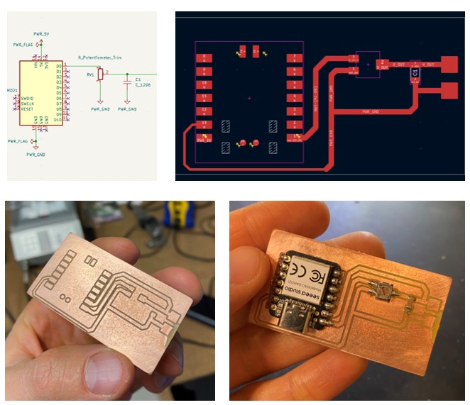
- Decided to use the SAMD21 in XIAO package for my microcontoller
- SAMD21 has a DAC, which will make generating input signals easier
- XIAO packaging makes it easier to solder onto my PCB
- DAC has max sampling rate of 350 kilo samples per second -> which means max freq of sine wav it can produce is 175 kHz
- Knew I wanted to use a potentiometer. Found a 10K pot in the inventory
- Choosing value of capacitor
- I want my cut off frequency to be 100 kHz
- If I want that to happen at midpoint of potentiometer (i.e. R = 5K), what should my value of C be?
-
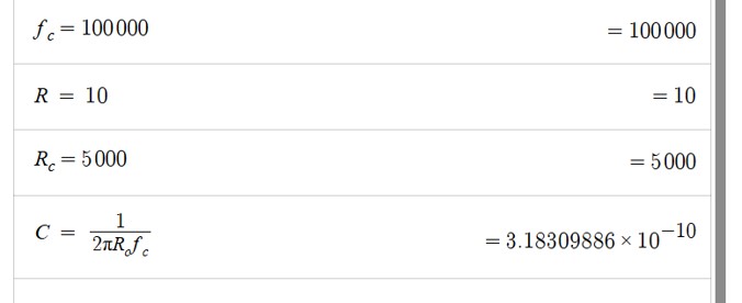
- Closest thing we have to 318 pF capacitor in the inventory is 100 pF.
- If C is 100 pF, what is cutoff frequency at mid point of potentiometer (5K)?
- 1/(2pi*50K*100pF) = 318 kHz
- This won’t work because its beyond 175 kHz...but it makes sense we got there b/c we divided C/3 and thus multiplied Fc by 3
- We need to increase the value of C from 318 pF, not decrease
- What is cutoff at 5K if using 1 nF C? 318 Hz okay, that should work!
- What is the max and min cutoff freq we can achieve by adjusting our potentiometer if we are using a 1 nF capacitor?
- R_min = 0.3 Ohm -> 5 MHz
- R_max = 10.45 K Ohm -> 152 Hz
- That’s plenty of range to demonstrate different cutoffs!
Step 5: Code
First, I needed to follow this Tutorial from Seeed in order to load the SAMD21 board into the Arduino IDE. Then I figured it would be easy enough to find some code to generate sine waves, taking advantage of th DAC's full from ~0 Hz to 175 kHz!....what a silly thing to think!
- First, I tried this tutorial from Sparkfun for their SAMD21 breakout board
- I thought this was promising until I tried to alter the frequency in the code and saw no impact on the output signal
- a closer look at the code showed me that although there was a frequency variable declared, it was never used!
- Next, I googled “arduino sketch SAMD21 sinusoid output” and was surprised to see that google auto-generated some code using AI, but this was also garbage
- Finally found a blog with some much better code (link).
- It generated clean sinusoidal signals from 17 Hz to 1000 Hz
- This is not nearly the range I had hoped for (up to 175 kHz), but it should be good enough!
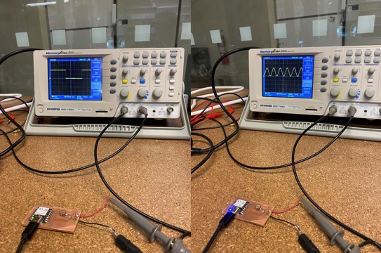
Step 6: Testing
My plan of attack was to set the cutoff frequency of my filter at 318 Hz (potentiometer at midpoint = 5k) and then show that frequencies below 318 Hz should "pass" and frequencies higher than that should get attenuated. Alas, try as I might, I couldn't get this to work. All frequencies I was able to produce were the same magnitude at the output of my filter. Changing the resistance seemed to have an effect on the magnitude of the output, but this was independent of frequency.
I tried swapping out the capacitor (changing from 1 nF to 1 uF) but this was rather undirected. Essentially, I was out of time by this point. My next step would have been to cut the trace going from the output of my filter to an analog input of my microcontoller, for I fear that this was having an impact. But alas, that will have to wait for another time!
NOTE: Check out my Week 9 post for the redemption of this circuit.
All files for replicating this work can be found here.
Acknowledgements
So many people to thank this week!
- Sara, for your help with re-working my website and teaching me how to use the Carvera
- I would like to further recognize my use of code based on Sara's repository
- both my new home page and sub-pages are based on the structure she showed me.
- Anthony and Dimitar for your insights on my PCB design
- Matti and Miranda for your KiCad tips and tricks
Return to Home Page