Final Project
Idea
The idea came from my recent experience participating in a hackathon. During this event, I had an idea with my friend Leo that we can build a wearable device that listens to conversations and provide live feedback through haptics or red/green signals. Our vision was that we could use these devices in challenging scenarios such as dating, professional presentations, or parent-child conversations, where users might not know how to express themselves properly. We hoped that the wearable device can act as a coach to help users become a more confident speaker.
Here's a demo of what my solution
The wearable I design will be more subtle hopefully, with small vibration that will let the user know that they are saying something wrong.
Built-in Microphone
Advanced MEMS microphone technology that listens to conversations in real-time. The ICS-43434 digital microphone captures clear audio with omnidirectional sensitivity, enabling the device to analyze speech patterns and provide instant feedback during conversations.
Heart Rate Monitoring
The MAX30102 sensor continuously monitors your heart rate and blood oxygen levels. This biometric data helps the AI understand your stress levels and emotional state during conversations, providing more personalized coaching feedback.
Haptic Feedback System
Subtle vibration patterns provide immediate, private feedback during conversations. The haptic system can signal when you're speaking too fast, using filler words, or when it's time to pause and listen - helping you become a more confident communicator.
Research
I started researching more about how to build a successful wearable device. My initial search landed me on the details of building my own ring:
I immediately learned how challenging it would be to build a ring device, which involves building a flexible circuit board that can fit in the small space of the ring. After consulting with , I switched my focus to developing a wearable necklace, which allows more room for error in my first time building something.
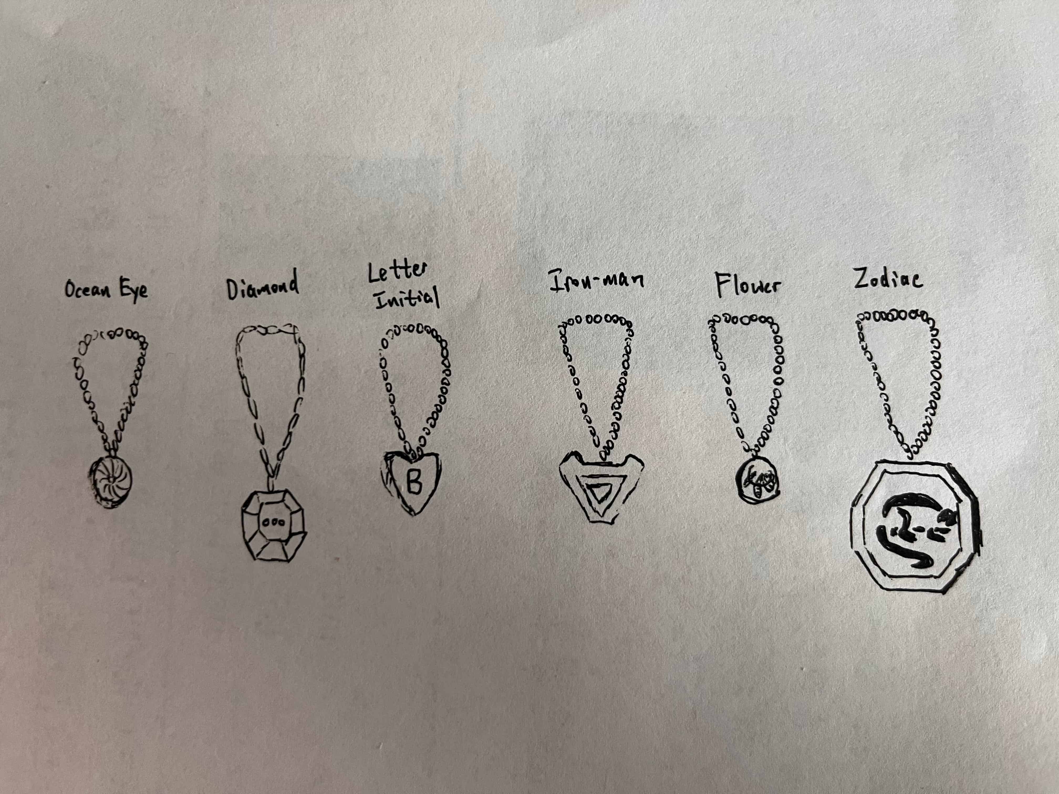
Necklace
I tried sketching different design of the necklace, mainly trying different shapes and contours.
Week 3 Planning
With 3D printing week starting and electronics design week coming up, I started to do more research in how I should design the case and the PCB board.
- SEEED STUDIO XIAO ESP32C3 WIFI+B
MAX30102: heart rate
ICS-43434: MICROPHONE MEMS DIGITAL I2S OMNI
HiLetGo: Display
Week 5
Here are the schematics design and PCB layout I worked on during week 5:
The next step is to iterate my design and see whether the PCB would fit in a watch or a necklace, which I would need to design an appropriate casing for.
Week 6
This week I learned to use the laser cutter to make the PCB board thanks to the help of Quentin and Sun.I then used the solder paste and heat gun to solder the microphone onto my board.
However, I wasn't getting any response with my microphone when I ran my code on the board. I figured out later that to use the ICS-43434, I need to drill a hole during my carvera cut. The holes are not in the edge cut files but needs to be generated independently through the Generate Drill Holes when plotting the outlines. Then, in gerber2img, I need to add the pth and npth files along with the edge cut so that it will merge all of the cut through parts together for Carvera to cut.
Week 7
After successfully working with a smaller sized board by using the laser cutter, I am getting a little more ambitious towards the final project. With the finals timeline approaching and the input and output weeks coming up, I did more in-depth research to confirm all of the components I can add to my device.
Here's the must-haves I need to use:
- Microcontroller: NRF5340-QKAA-R
- Round Display: 240x240 Round IPS TFT LCD Display 1.28" Capacitive Touch Circle Screen
- Battery: LI-PO
- Charging: PO-GO pin pads
- Flash: MX25U51245GZ4I00
- Mic: ICS-43434
- Haptics Driver: DRV2605
- Motor/buzzer: Precision Microdrives C10-100
- Heart Rate: MAX30102
- FCC Connector for screen: OK24M02404 is a common 0.5 mm pitch, 24-pin FFC/FPC connector
- Power management? Nordic nPM1300 PMIC for power and system management
Here's some nice to haves but I might not add if limited by space and time:
- Pressure sensor: DPS310XTSA1
- Motion sensor: LSM6DSV16XTR
- Time: RV-8523-C3
I need to design my PCB to be around 39mm in diameter to fit in normal watch cases. I am thinking to send my PCB design to a PCB house to get it manufactured at a higher resolution. I am looking to create a more old-school feel and a classical watch rather than a pure tech feel.
I got a sample watch case so that I can examine the casing better, and I might look to 3D print my own case to better fit the pcb. I might also look at molding & casting week to see if I can make the case from that week.
Midterm Review
Here's the system diagram for my project:


Tasks to be completed in order:
| Task | Deadline |
|---|---|
| Design the PCB and send to PCB house | 11/18 |
| Laser Cut MVP Board | 11/20 |
| Solder MVP Board Components | 11/23 |
| Design Watch Case & 3D Print | 11/25 |
| Design Wrist Band | 11/25 |
| Mold & Cast Wrist Band with silicone rubber | 12/01 |
| Embedded Programming Development | 12/05 |
Week 12
The pressure is finally catching up to me. This week I made a lot more progress. But still, I have a lot to do and I find that a lot of the design is hard to do without knowing how the actual components look like and how the PCB is going to come together. Therefore, I am struggling a little bit with how big the watch case should be, where I should have holes, and etc.
Designing the case
I followed this tutorial to start designing the case in Fusion 360. The key to making a watch case is having one sketch and using the revolve function to rotate around the center axis and generating the circular case. I made the design parametric so that I can adjust the design later on to fit the actual screen size, PCB size, and the wrist band size.
Ordering More Components
I placed a few more orders for the components that I will need for my project.
- Screen
- Motor
- Li-po Battery
- POGO-Charging
Charging Box
To implement more processes other than 3D printing, I am also thinking of developing a charging station where I can place my wearable on and it would start charging with the pogo pins. For this, I am thinking I can do wood cutting with vinyl cutting stickers to decorate it. I could also add LEDs and screen to further decorate it, but due to time constraints, I will likely just stick to getting the basic box completed.
While I do have a lot of the things settled, I definitely have a lot left to do, so I really need to get the PCB done as soon as possible to have time to adjust my case layouts and iterate on the case sizing. But for now, I might just start a print that's more lenient on the sizes and spacings. If I have time later, I can consider narrowing down for a more snuggle fit.
Week 13
Some New Realizations on PCB
Trying to finalize the PCB design this week, I realized I made some mistakes early on.
The first crucial piece is that MAX30102 is a 1.8V peripheral while my MCU is 3.3V. I learned that I need a voltage regulator to convert the 3.3V to 1.8V in order to power my peripheral. I also need a logic shifter for sucessful I2C connection.
In addition, I learned that I can use smaller sized resistors and capacitors to save more space in my PCB design for a more compact fit. For example, I have been using 1206 capacitors and resistors, which has dimension of 3.2mm by 1.6mm. Instead, I can use 0603 with dimension 0.6mm by 0.3mm to reduce the space. Thus, I replaced all of my resistors and capacitors to the 0603, which allowed me to narrow the board down with diameter to approximately 51mm. The main block for further narrowing the size is
Picking the screen
I originally bought a 1.6 inch QSPI touch display. However, I realized that this screen requires many pins, which could be challenging as XIAO ESP32S3 only has 11 GPIO pins on the sides, plus 4 more on the back that needs to be soldered with solder paste. These pins on the back are also harder for me to design since my MCU needs to be at the border of the PCB board. When I bought my first screen, "QSPI 1.6 inch 400x400 Round Circle Screen IPS TFT Display Panel ST77903", I just thought I wanted a big round screen with touch capabilities. As nice as that sound, I realized that I need around 13 GPIOs, which would take up too much pins.
Edit: Upon revisiting this part towards the very end of the project, I am wondering if I need all 13 GPIO pins on the screen. Consulting with ChatGPT, there are some pins on the screen that I don't need to connect. For example, the LEDK and LEDA needs 1 GPIO only if I want PWM control; otherwise I can connect directly to power/GND. Another example is for Quad SPI or QSPI, if I only want single data line, then I only need 4 GPIOs and I can safely ignore SDA0 to SDA3, but if I want to use QSPI for 4x faster data transfer, then I would use these 4 extra 4 GPIOs so that 4 bits are transfered simultaneously each clock cycle. These are some of the subtleties I didn't pay attention to in the beginning, which caused me to switch to another screen.
I switched my eye to another screen designed by Adafruit, Adafruit 1.28" 240x240 Round TFT LCD Display with MicroSD - GC9A01A with EYESPI Connector. This screen is smaller, and does not have touch capabilities. More importantly, it only needs 7 GPIO pins, which gives me just enough flexibility to add in my I2C peripherals and I2S mic.
Battery Management
Battery management is another thing I learned. I originally thought I just need to connect my pogo pins directly to the battery and the battery to ESP32-S3 and I'm done. Little did I know that I need a dedicated battery management component to monitor status such as remaining battery, battery temperature with a thermister, and etc.
Two Boards?
While I want to have as complete of a project as possible, I do realize that some of the components are more challenging to implement. Also, after laying out the 18 pin FFC connectors and the JST connectors in KiCad, I learned that they require a lot more space than I expected. There's no way that I would fit everything in one board without extending the diameter of my PCB.
Learning from the cake board design implemented by Tyler in machine week, I learned that we can make multiple boards and connect them. Thus, I decided to separate my design into two board components. One board is going to contain the MCU and all the smaller components that I need to hit my MVP goals. The second board will contain the battery, charging, screen, and all additional features that I would like to implement but might not if time is a major concern.
Eventually, thinking about limiting the height of my project and the fixed size for male and female connectors, I gave up on this idea and back to fitting everything on one board.
Final Sprint
Going into the final week of the semester, I had very little time left and with many things going on in the lab, I could only squeeze out all of the time I have left and tried to pull everything together.
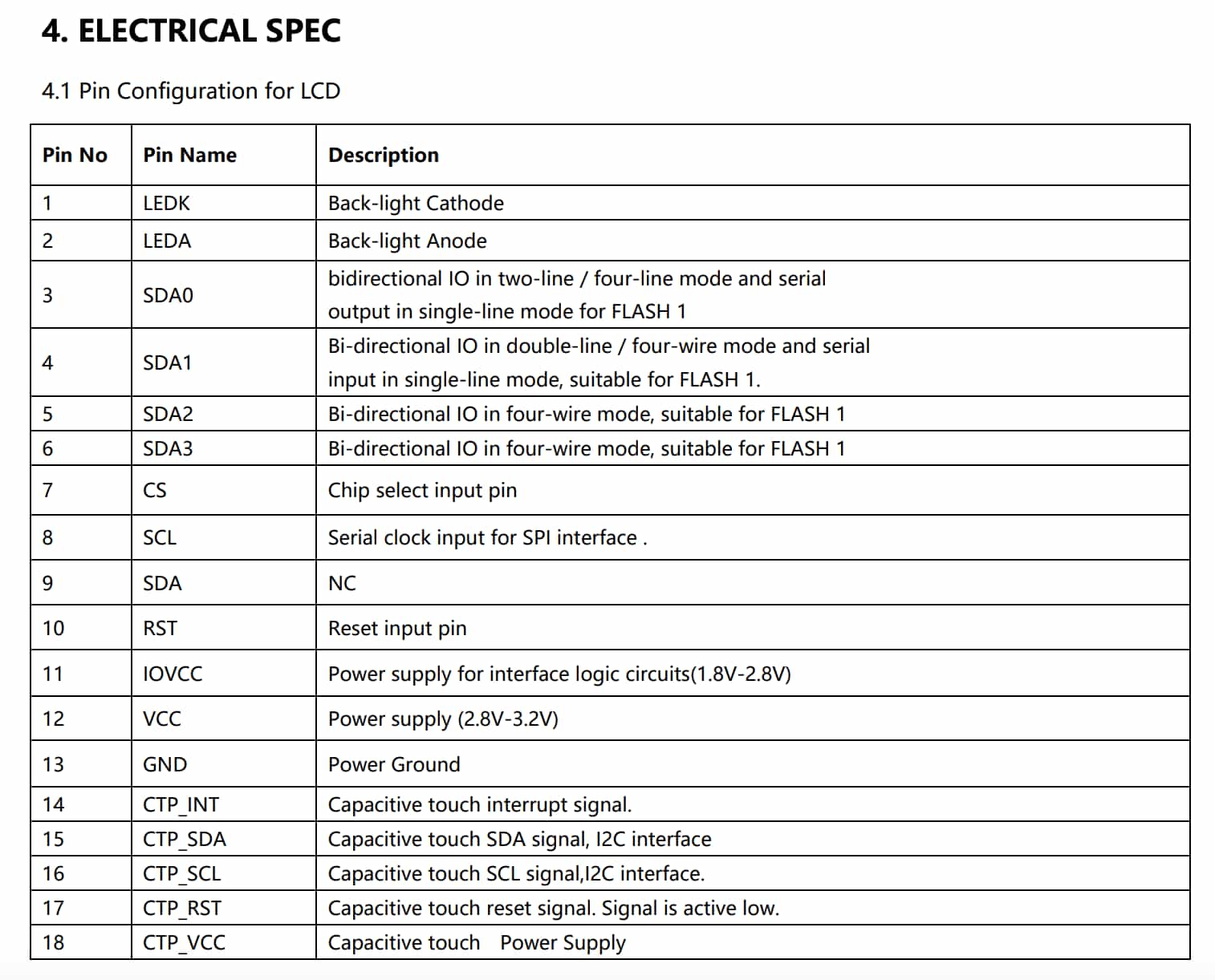
PCB Iterations
Here is version 1 which has the full design I would like to have:
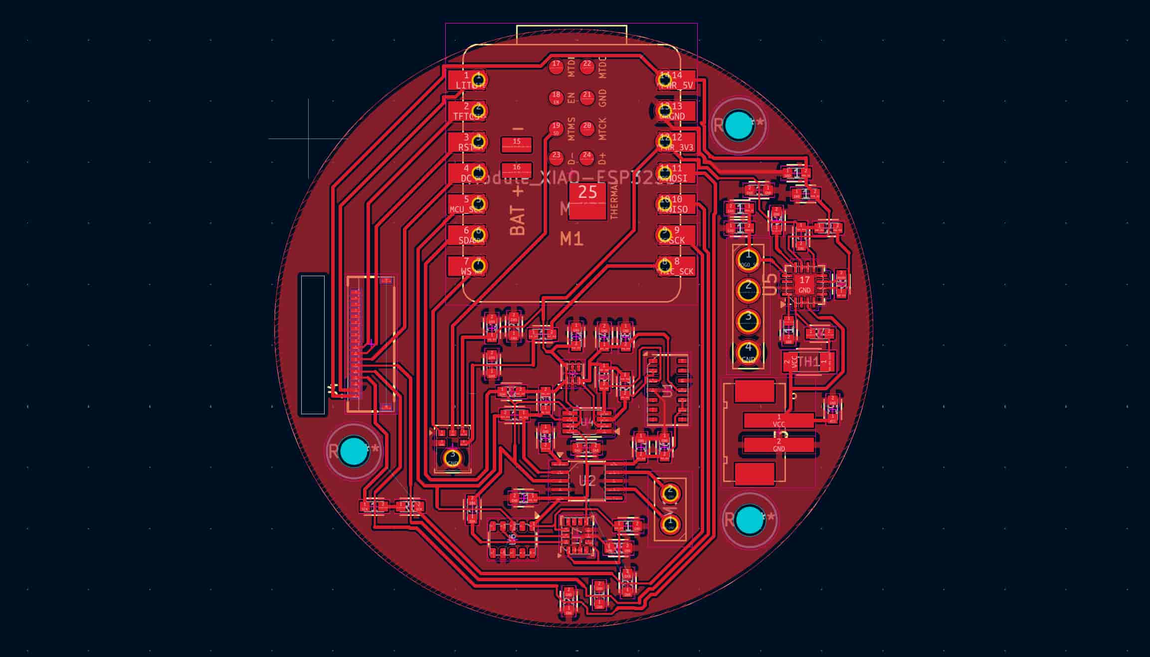
Version 2: I need to add a hole on my PCB for the battery wires to pass through. As a result, I removed the MAX30102 module because it requires a dedicated power and logic shifter.
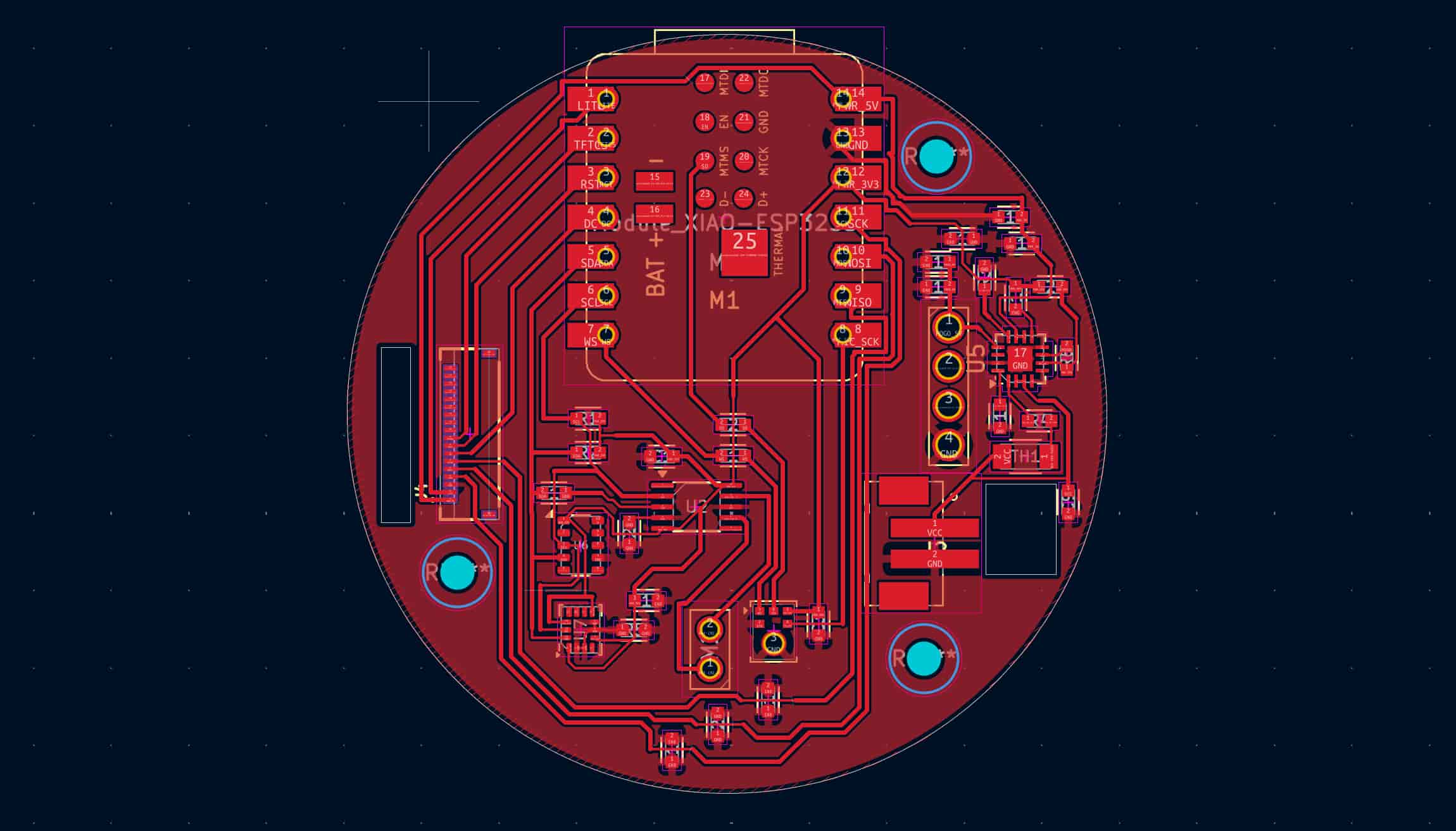
Version 3: I removed the battery related components because I'm not too famaliar with how battery works and I could use the extra space to connect all the ground planes. I didn't realize there are many islands in my design and I needed a lot of 0ohm bridge to connect the islands.
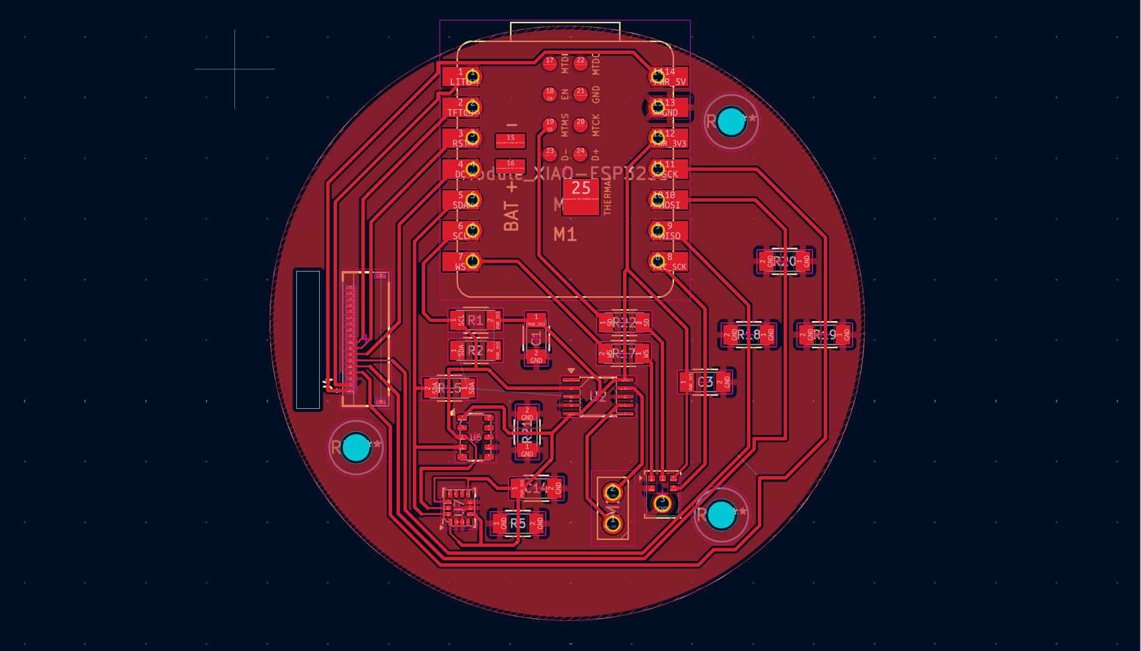
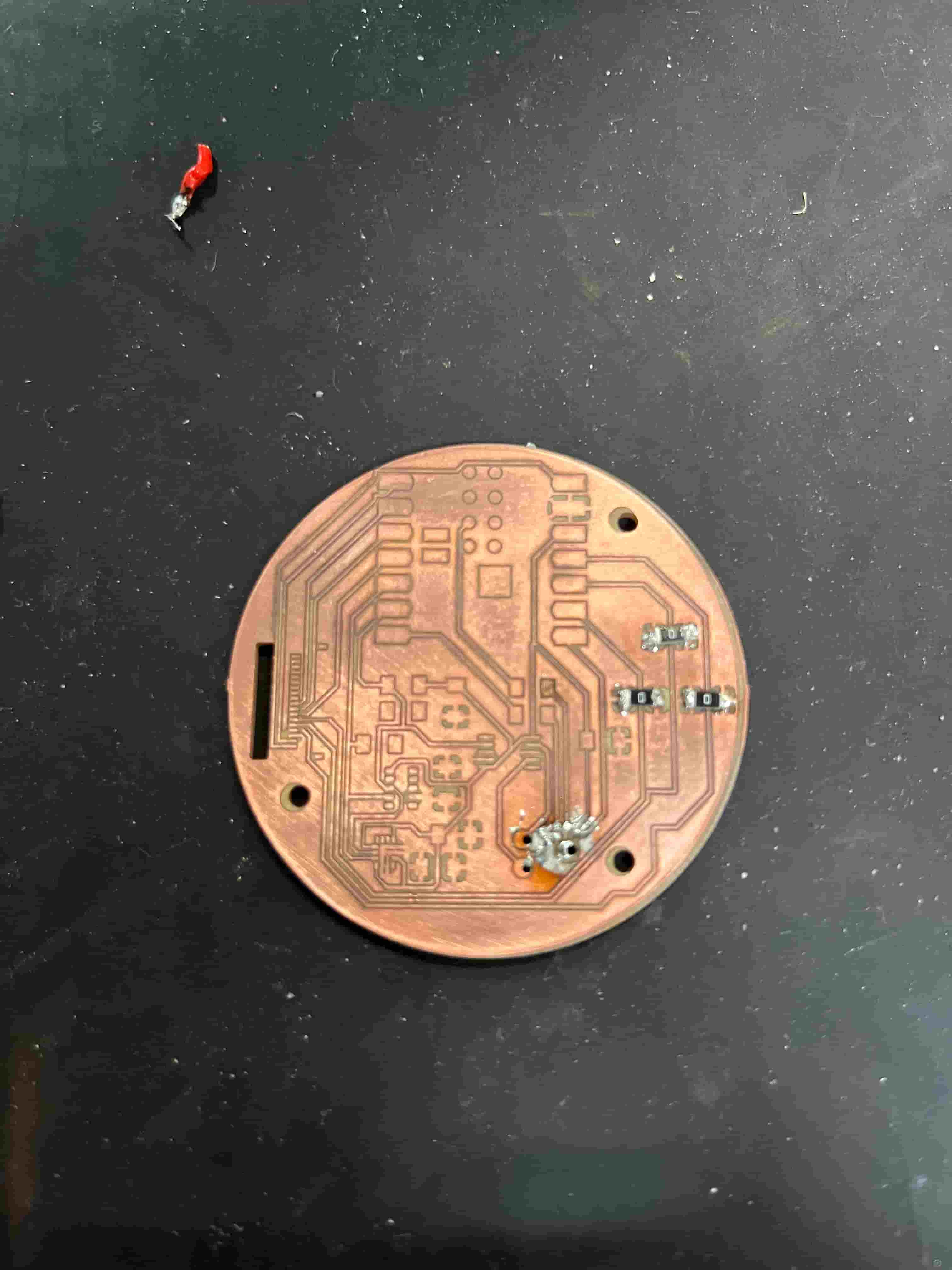
Version 4: After the soldering with ICS-43434 failed, I decided to use the mic that came with ESP32-S3 Sense. So I removed the mic component from the PCB and added the RGB LED as a replacement output device.
Version 5: The soldering of the 18 pin 0.5mm pitch FFC connector with the help of Anthony also failed. This came after me soldering almost everything onto the board and realizing there are many weird shorts. After desoldering the ESP32-S3 with the help of Miranda, I could not figure out where the short was coming from. Eventually, I isolated to the bottom of the FFC connector, where I have traces coming from under the component and being close to the mechanical pin. The MISO, MOSI, and SCK pins are shorting to ground, which supports my hypothesis because they're right next to the mechanical pin.
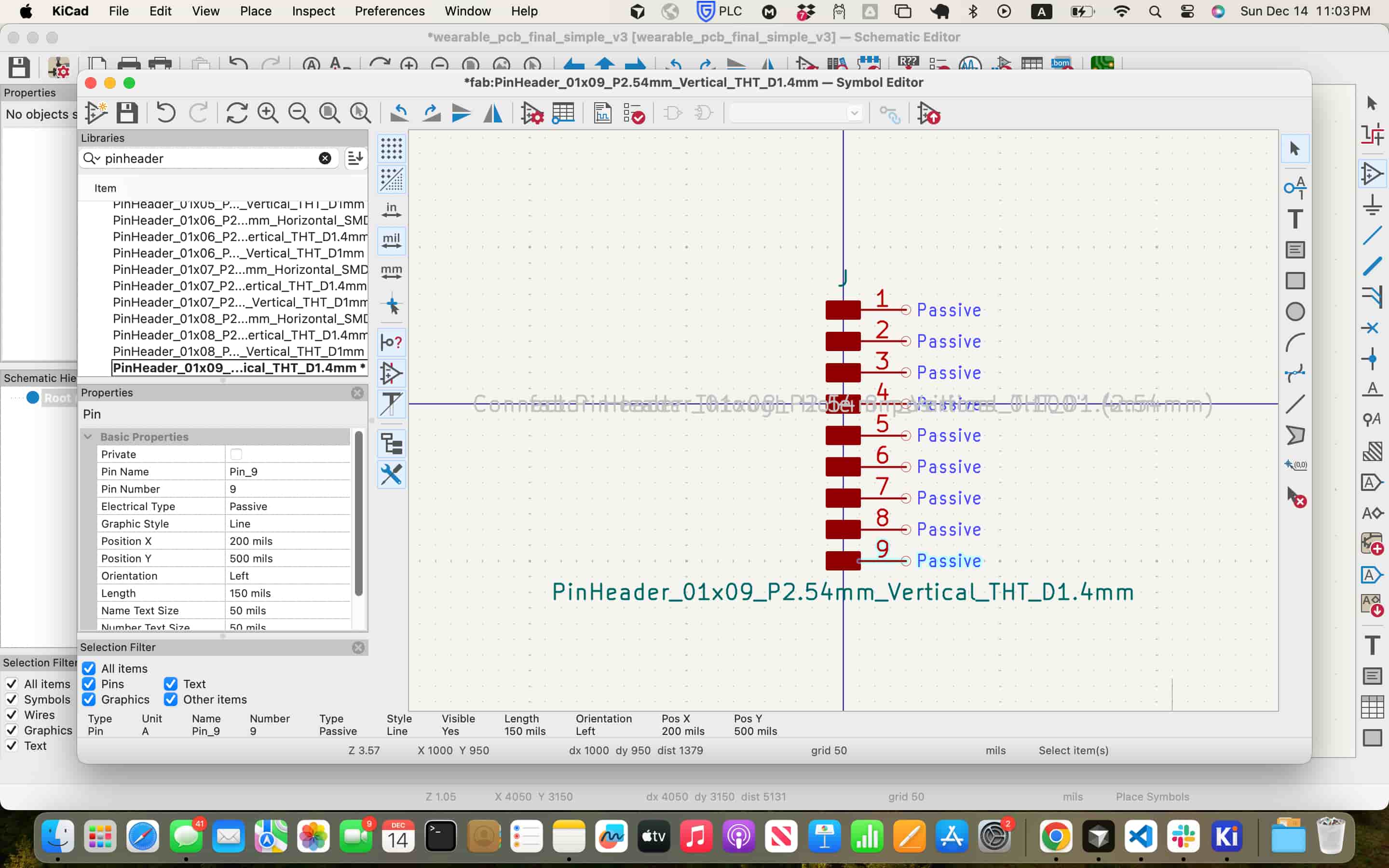
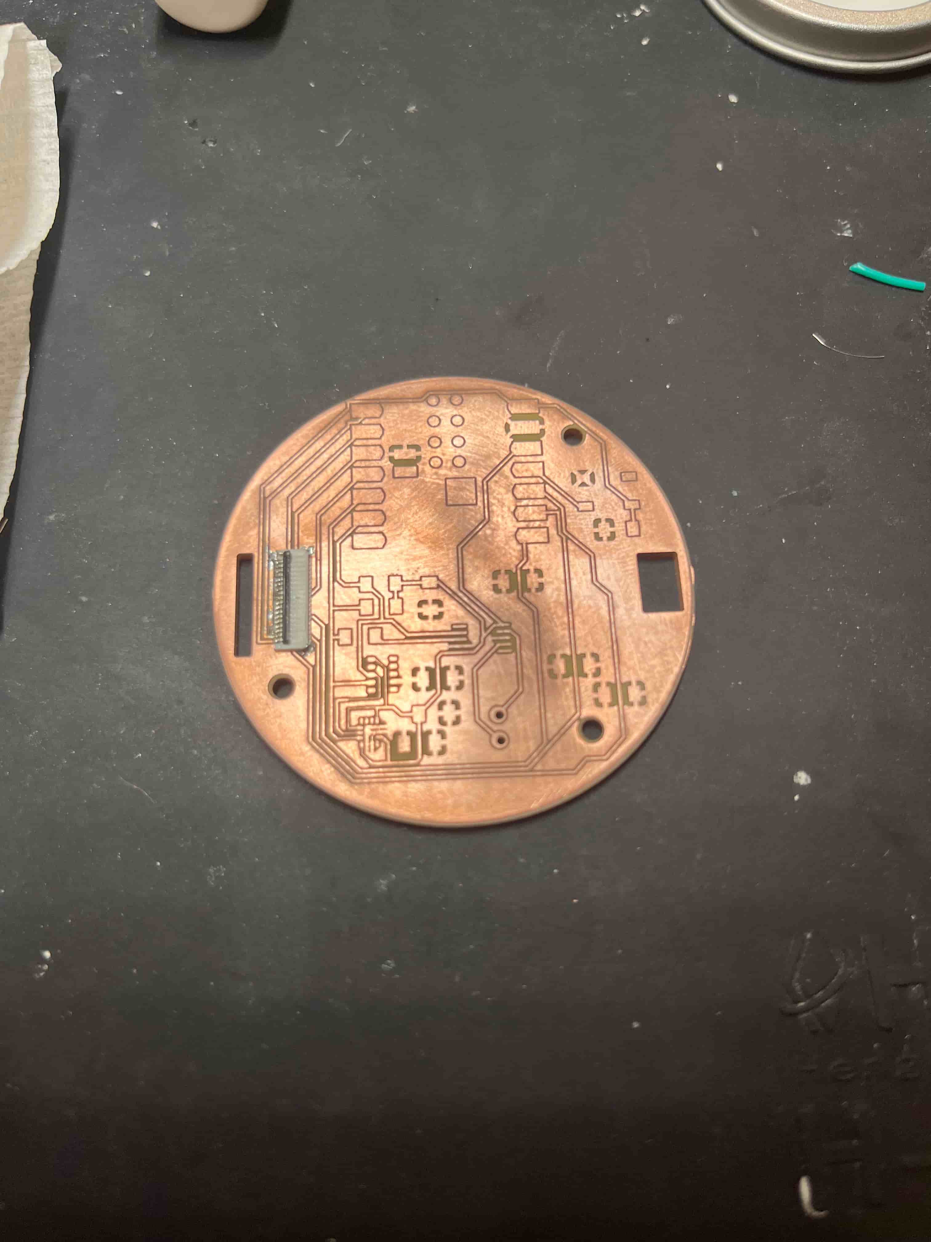
Since the screen requires 11 pins and the library only has up to 8 pins in Kicad, I modified the symbol and footprint library to include 3 extra pins.
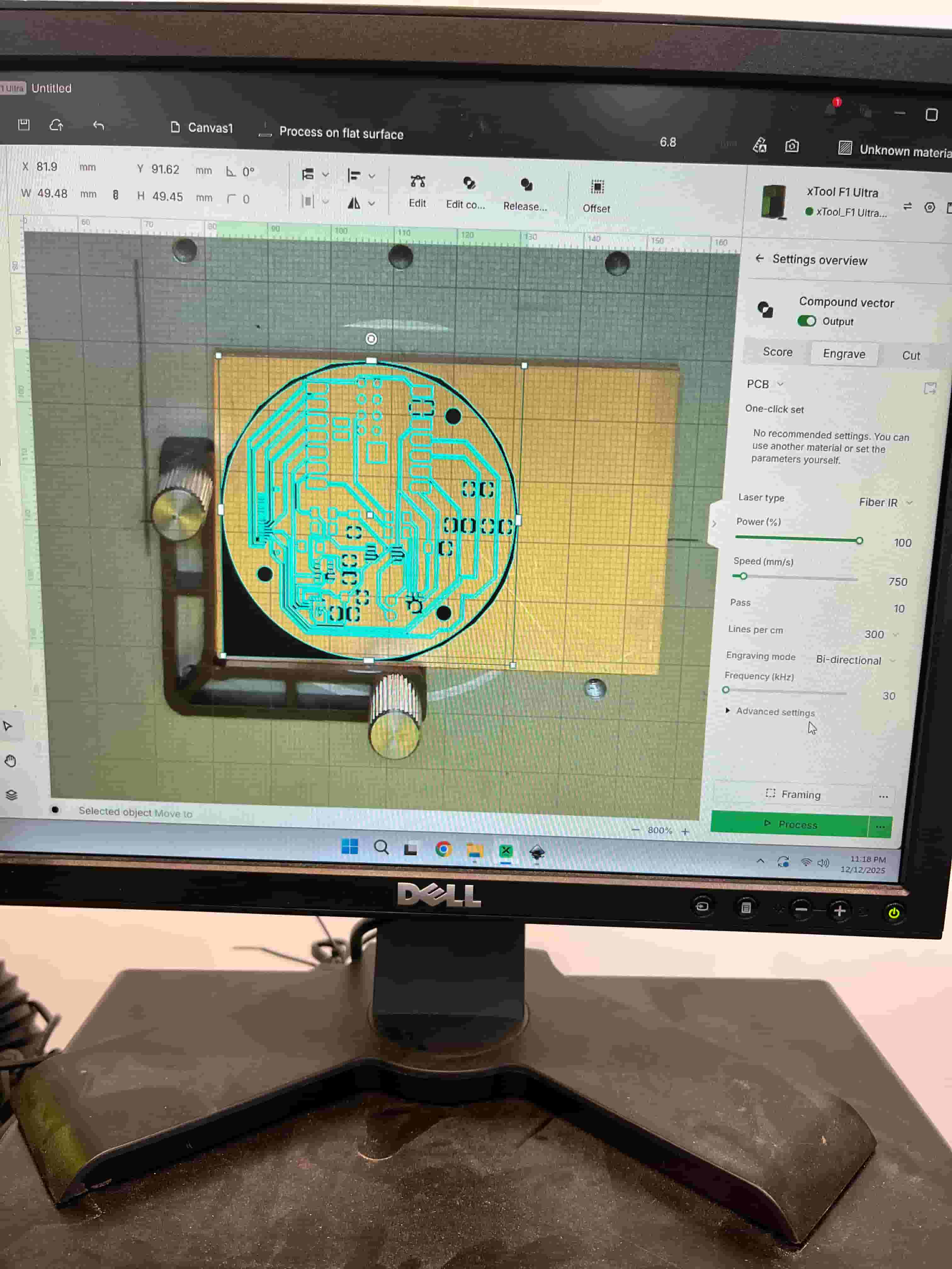
Aligning Carvera and XTool F1 Ultra
I needed the Carvera to cut my edge cuts and the laser cutter to cut my traces since some of the components I used such as DRV2605. However, this posed a problem because I was trying to cut a circular board, which is hard to align when I take the board to the XTool laser cutter, since there's no clear reference for the orientation of the board. This is a particular issue due to my usage of IC-43434 and a linear motor, which both required through hole pins and need the traces to perfectly enclose the through holes.
In the beginning, I tried to align my traces image in the XTool software perfectly above my board, but the laser cutter has some alignment issues so that even when I place the traces exactly on the board image, the traces would be slightly down to the right. This prevents the connection between traces and small through holes. It was even harder since my circular board was hard to orient upright, so I need to rotate the traces in the software to account for it.
However, this method proves both time consuming and inefficient. Even with multiple boards for trial and error, I was still getting low success rate. I feel that
I knew I needed to add a right angle for easier configurations. So I added a rectangular corner at the bottom of the traces in XTool software. This is a little bit risky because Quentin said before to avoid large area of laser cut engraving as the high temperature could lead to burns. I tried to remove the unnecessary engrave on the other three corners and kept a close eye during the engrave.
Then, I measured the distance from the edge to the circle at the left and at the bottom, before setting the origin on Carvera to that distance.
Even with this, there's still some misalignment, but the traces around the linear motor has a thin connection, which could work. I tried soldering the IC-43434 onto the board with heat gun. Unfortunately, I put the heat gun for a little too long, which removed the cap from the mic. When trying to desolder the mic from the board, I accidentally ruined the board.
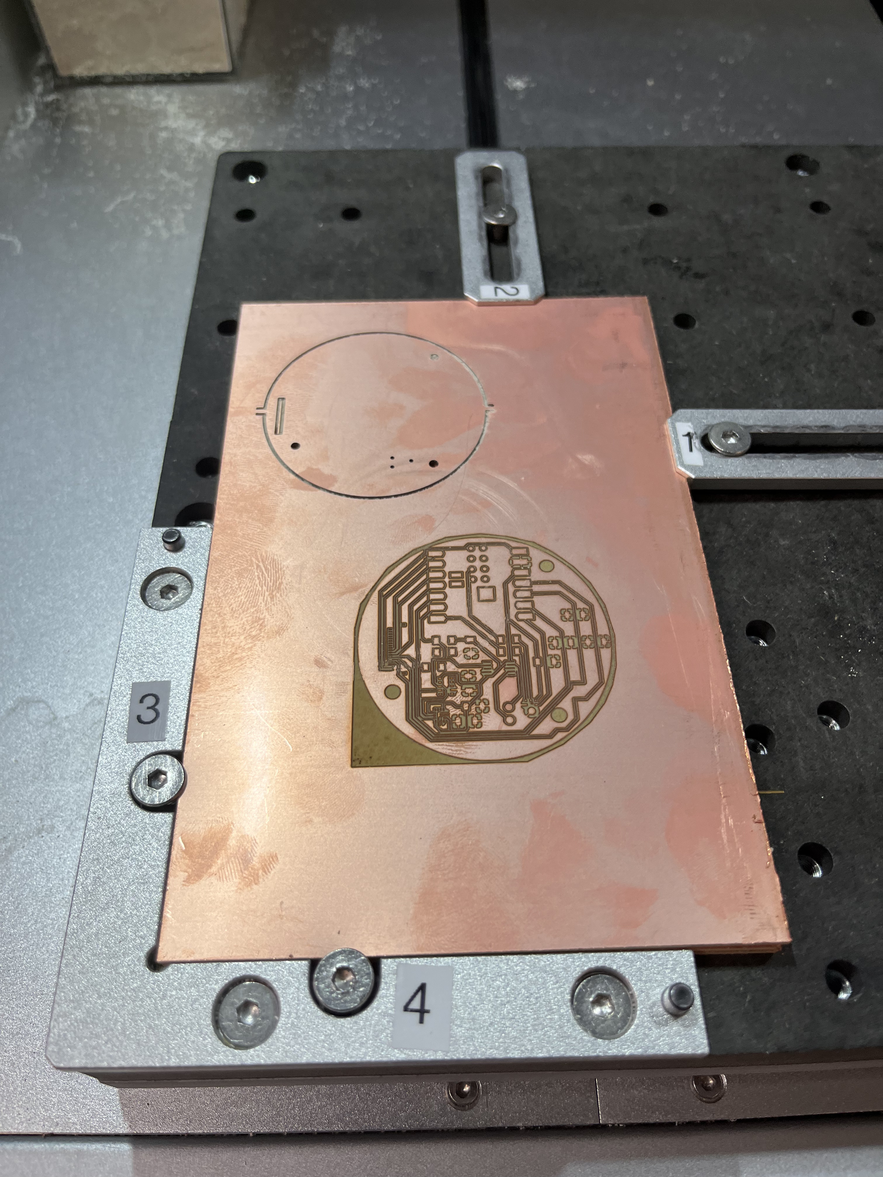
I then tried another way. I first cut the edges and through holes on Carvera, then without removing the board, I take the whole rectangular board to the laser cutter. I would cut the same design on two different boards so I can use the first board to calibrate the location, and the second board to actually engrave the traces. I found that after placing the image perfectly on top of the board in the software, I pressed the left button 6 times and the up button 4 times to achieve near perfect alignment on the actual laser cut.
However, the board production process is very time-consuming, taking approximately 2 hours per board.
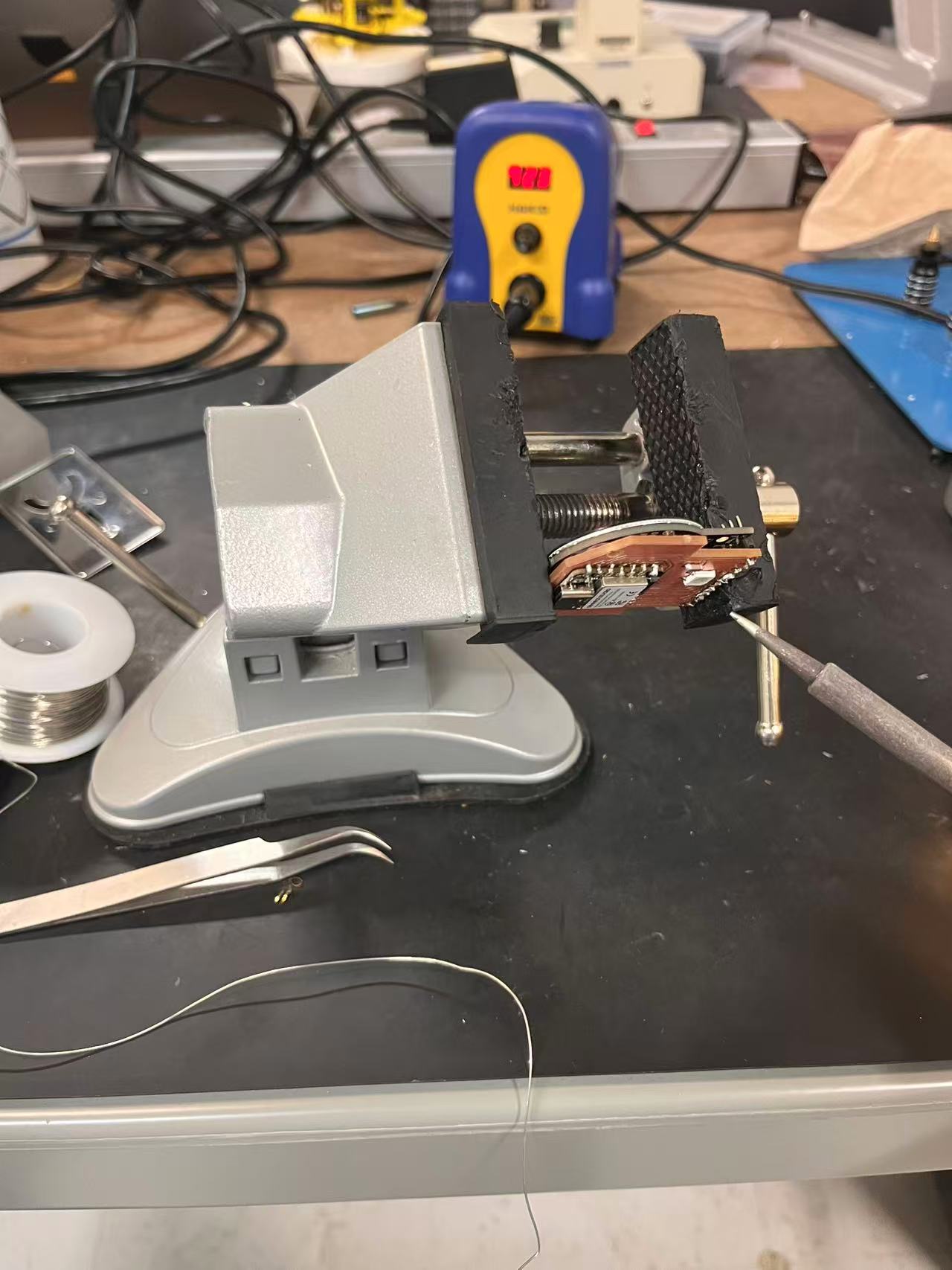
Soldering
The first try was working on the ICS-43434, but because I applied the heat gun for too long, the top case for the mic was removed by the heat, and I had to desolder the mic. Without the case, removing the bottom part was very challenging. With the help of Alan, we applied more solder and removed them all together. However, this damaged the board itself.
With the help of Anthony, he helped me carefully soldered the FFC connector on, and showed me how to use the microscope to check for bridges between the pitches.
I then went on to soldering the resistors, capacitors, and the ESP32-S3 MCU. However, using the multimeter to check for shorts, I found out that the SCK, MOSI, and MISO pins were shorted to ground. After a series of debugging, including desoldering the MCU with the help of Miranda, I limited the problem to the FFC connector as all three traces go under the connector and around one of the mechanical pins of the connector. I tried to use the heat gun to resolve this, but it was challenging without melting the plastic of the connector.
Without much time left, I produced a more spatious board. However, the THT dimension is slightly larger than the pins of the screen, so I needed to clamp the PCB upside-down to prevent the hot solder from going through the hole and melting the plastic under.
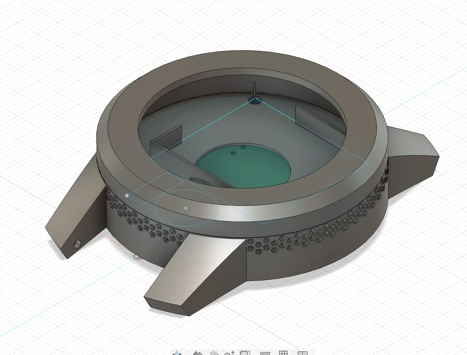
Watch Case Iterations
For the watch case, I iterated a few times as well.
Version 0: For this version, I just had the basic outline completed, testing how functions such as revolve could be used to make a design for my case.
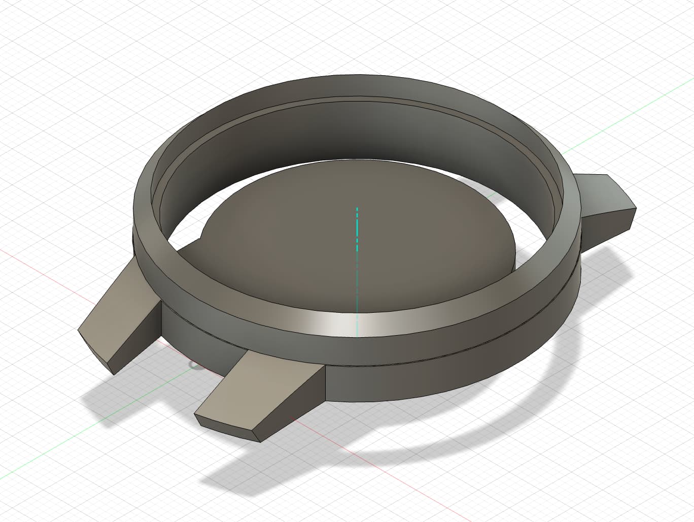
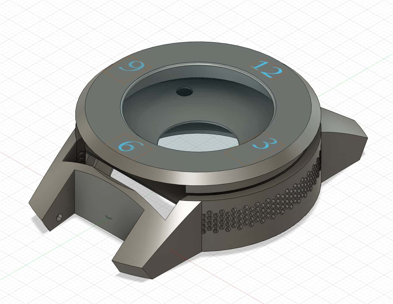
Version 1: This is a more complete design that I have. I added the bezel and the base. For the base, I also used Fusion 360's threading tool to create M50 threads for the base to be rotated into the case. I also added the step file from Kicad to visualize where I need to place my drill holes and how the PCB would be attached to the case. I also used the emboss feature in Fusion 360 to add the honeycomb shape to the case, which provided holes for sound to pass through.
Here is version 1 with the bezel:
 Here is version 1 with the threaded base:
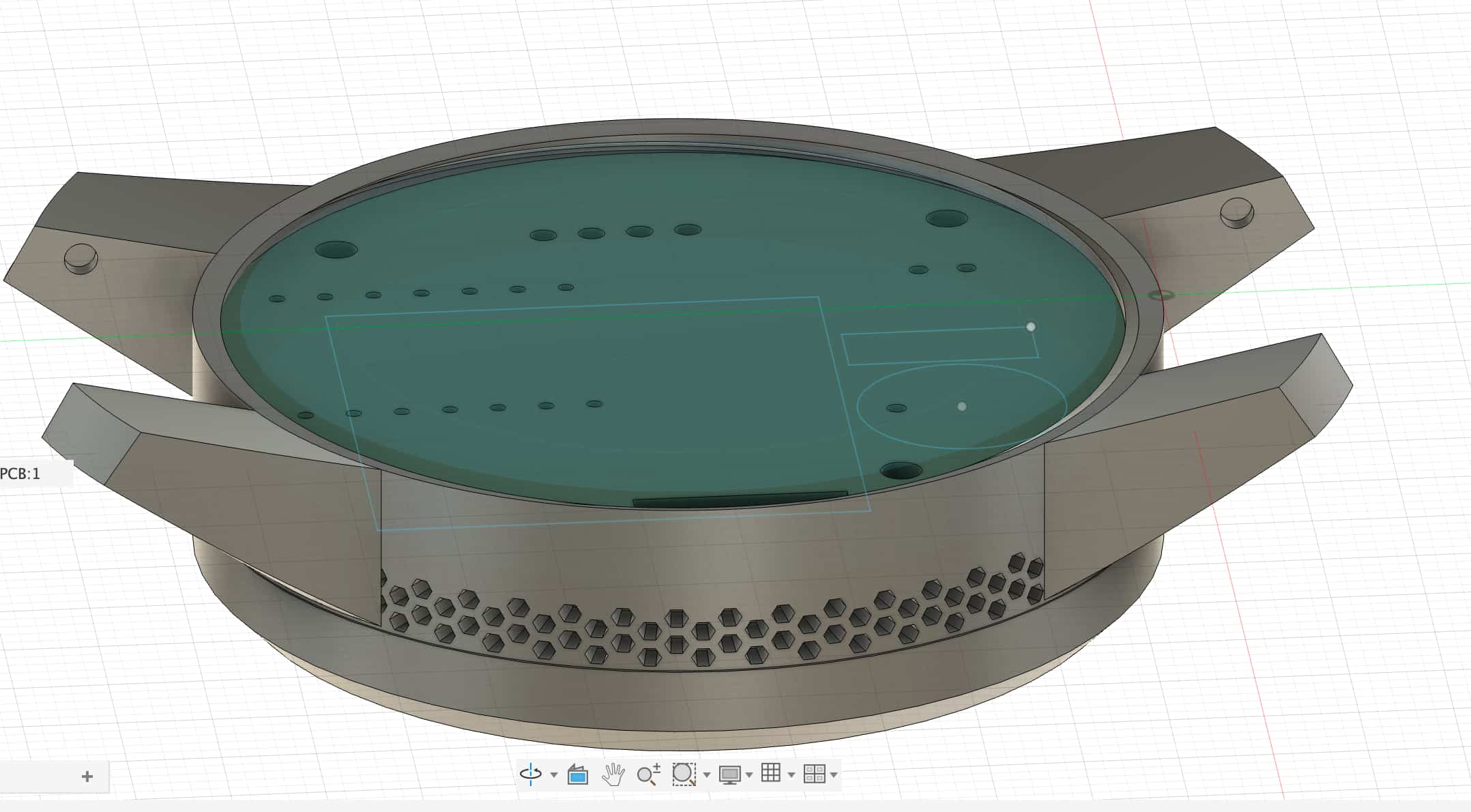
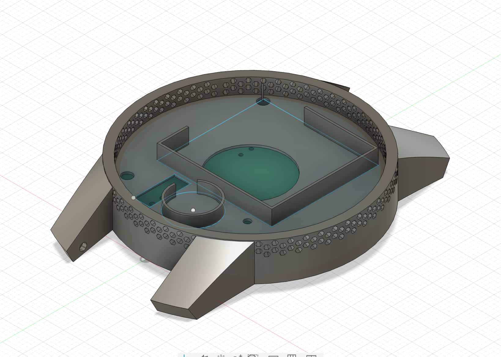
Version 2: I mainly changed the batter holder size in the middle layer. The battery turned out to be 31mm by 30.5mm while the advertised dimension was 27mm by 24mm. I also extended the case of my height after doing some calculations on paper to see the total height of stacking my PCB, screen, and battery, as well as the component height that goes onto my PCB. Another thing I changed was adding a rectangular extrusion on one side of my case because the Adafruit screen was not perfectly round, but has a rectangular bottom for through hole pin connections.
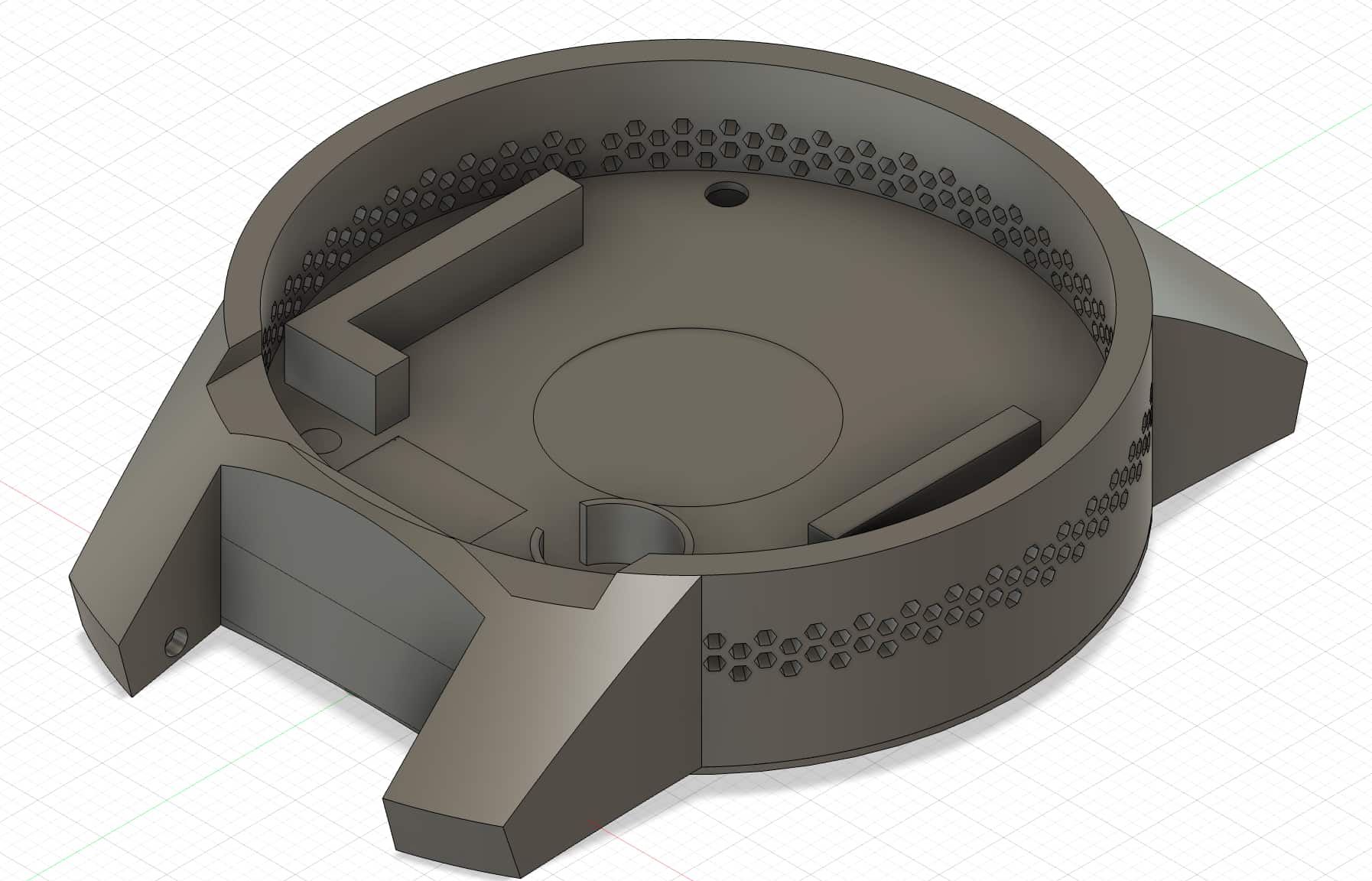
Version 3: I moved the haptics driver to the base. I also adjusted the battery holder height to go right under the screen to offer the screen support as well. The screen also has a few layers that I needed to measure carefully. On the top of the screen comonent is the actual lcd screen, in the middle is the PCB layer, and at the bottom there are FFC connectors, SD card holders, and resistors and etc. Thus, it was important to see where to place the pillars to support the screen. You can see the pillar in the middle has lower height because the FFC connector goes right there and could lie perfectly on the pillar.
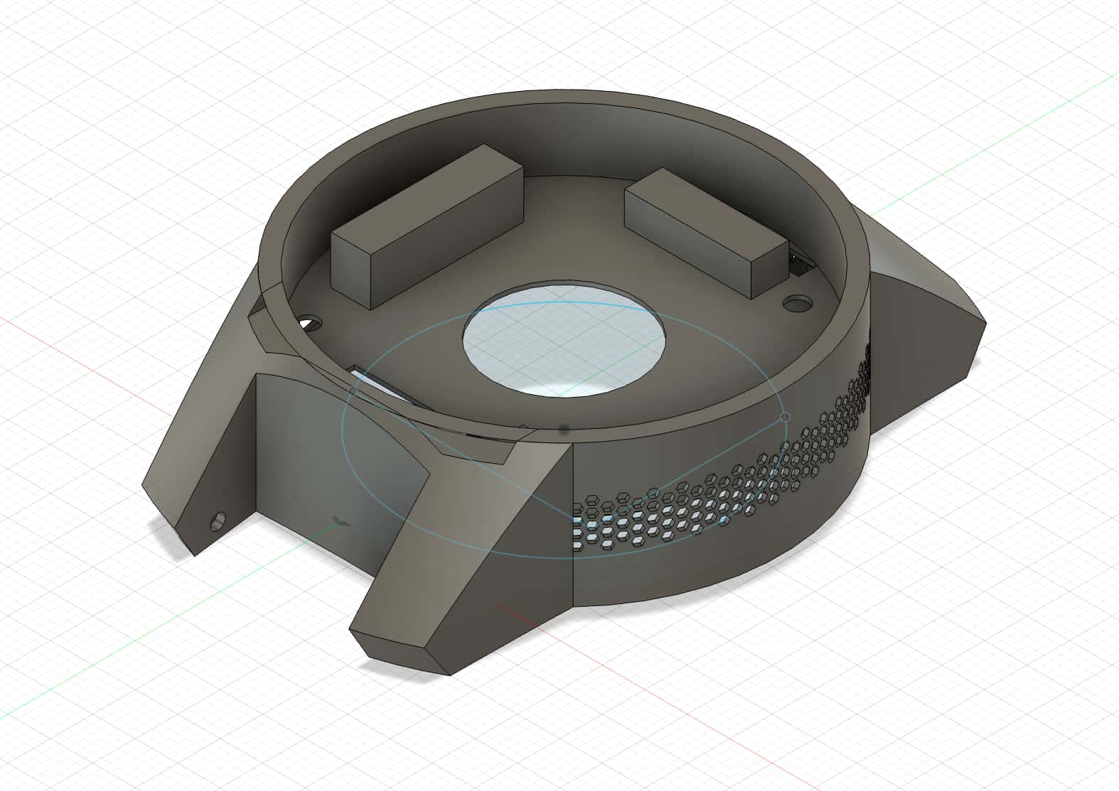
Version 4: This is the final version of the case used. I removed the battery and haptics holder as those are not used. I then cut the middle layer out for space to use through hole pins to connect to the screen. I also added text to the bezel to export the top layer as dxf file.
3D Printing
I learned to use the Form Fuse nylon printer following an online tutorial and using the sand blaster to remove the powder afterwards. Each print takes approximately 2 hours and 1L of powder, with 2 hours of preheat prior and 2 hours of cool down after. So around 6 hours in total for the print.
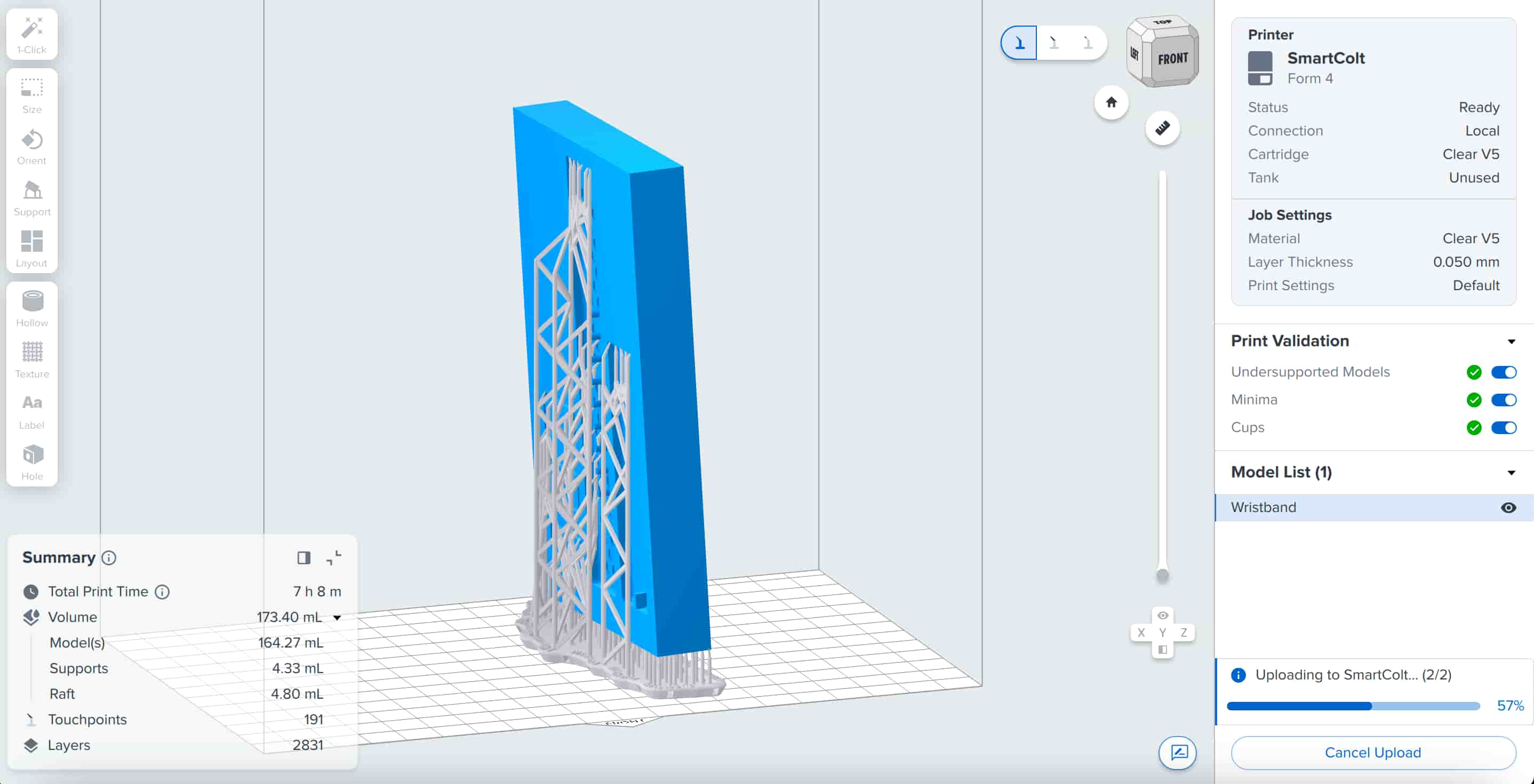
I also used Formlab's Form 4 SLA printer to print the mold. This print takes around 7 hours for 0.05mm layer thickness.
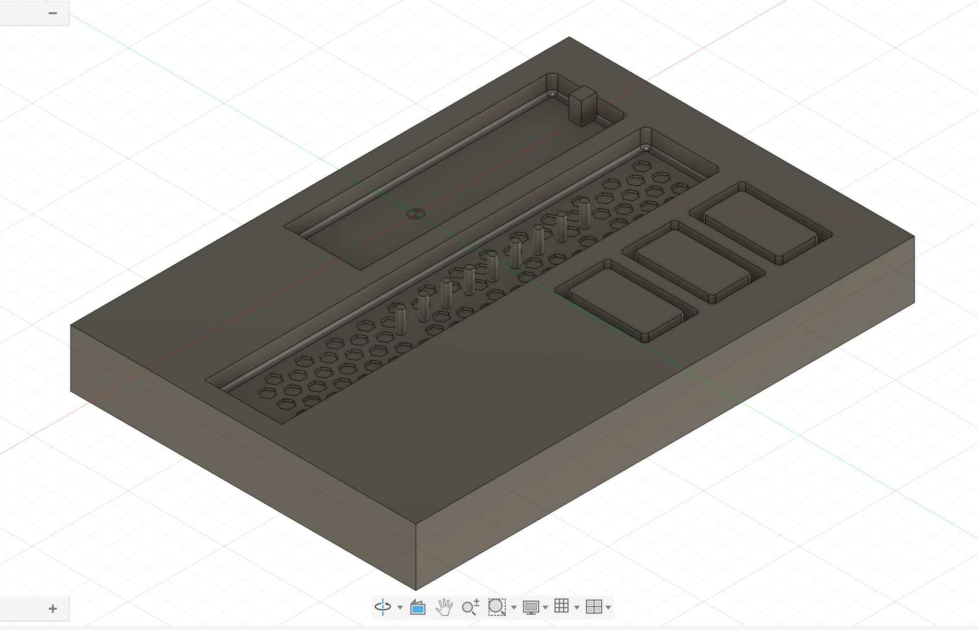
Wrist Band Iterations
I first created the positives design following Tyler Hill's experience in his molding and casting week.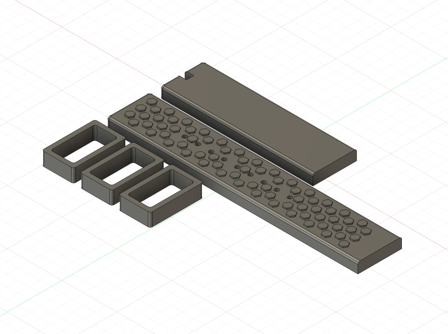 I then added a rectangular box, and used Fusion 360's combine + cut to make the negative mold.
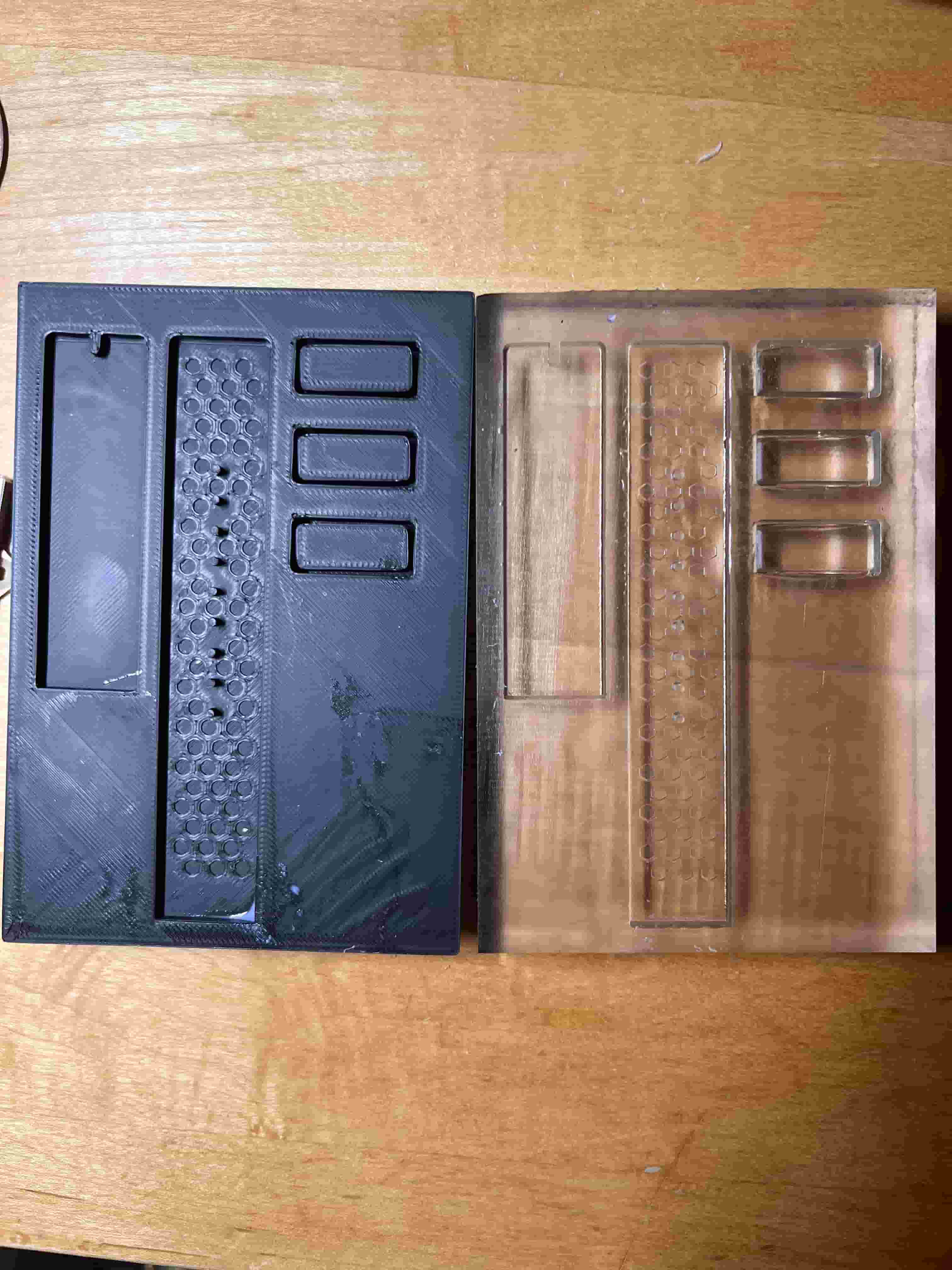
 I then printed a mold in both Prusa and Form 4 with material Clear V5. Comparing the results, I decided to proceed with the Form 4 printed mold, which has finer details for the honeycomb extrusions. I used Oomoo's silicone gel, which takes approximately 6 hours. With Dimitar's extra casting material, I slowly poured in the cast to prevent too many air bubbles from forming. After six hours, here are the results.
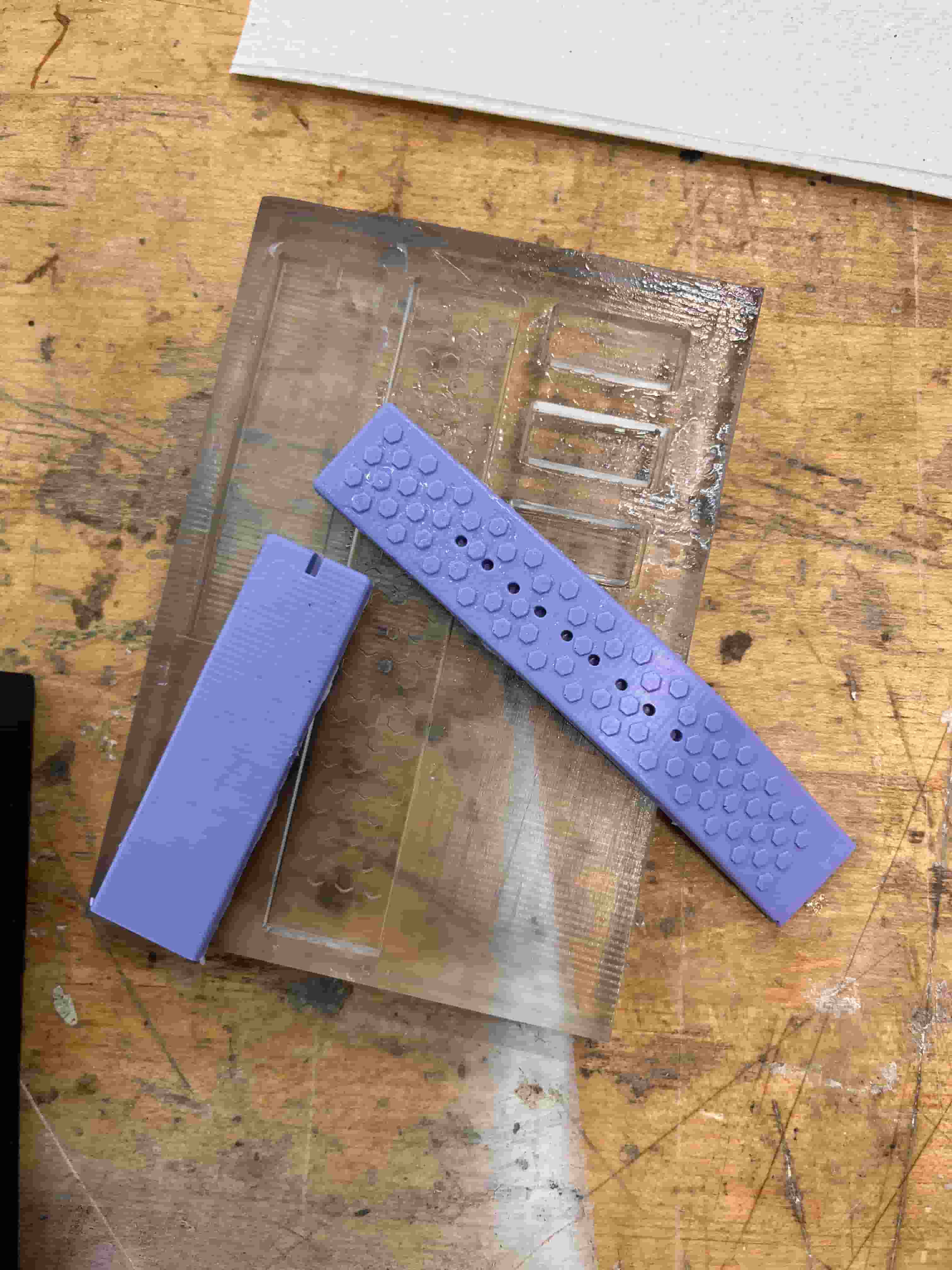 Noticing the band is a little too thin, which might be difficult for me to drill the holes for the pins later, I did a second iteration with a thicker band height. I also noticed that the holder was a little deformed on the mold, which might be due to the thin width I gave it and the vertical orientation I printed in. Thus, I increased the width of the holder from 1mm to 2mm, and I also printed this horizontally and face down. I also added some extra height to the pin holes to preent the holes from being covered by the cast.
Here's how the mold came out compared to the first one. The difference is very subtle.
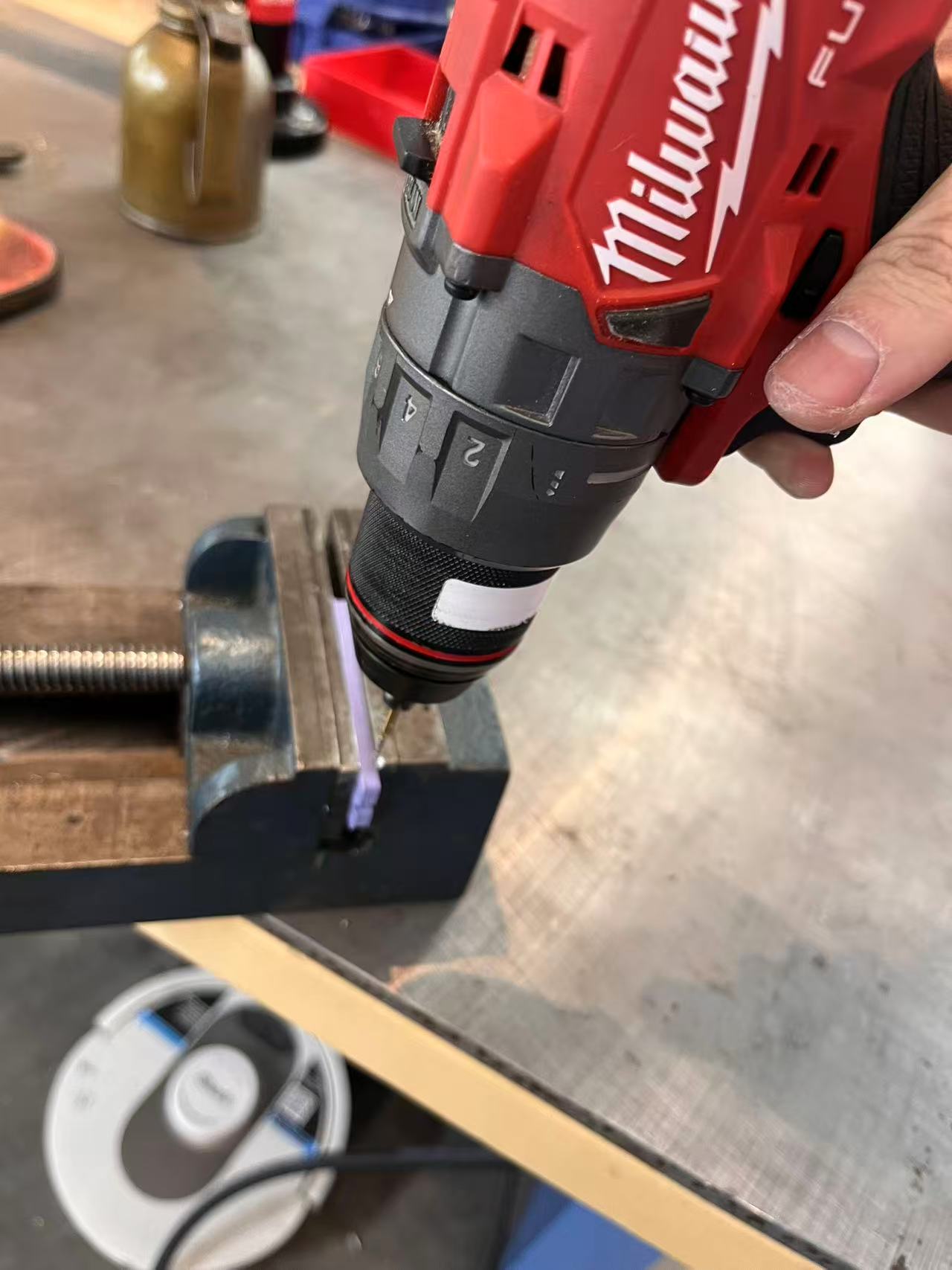
Finally, I used the dremel to drill tiny holes through the edge of the band so I can insert the pins to connect the band to the watch.
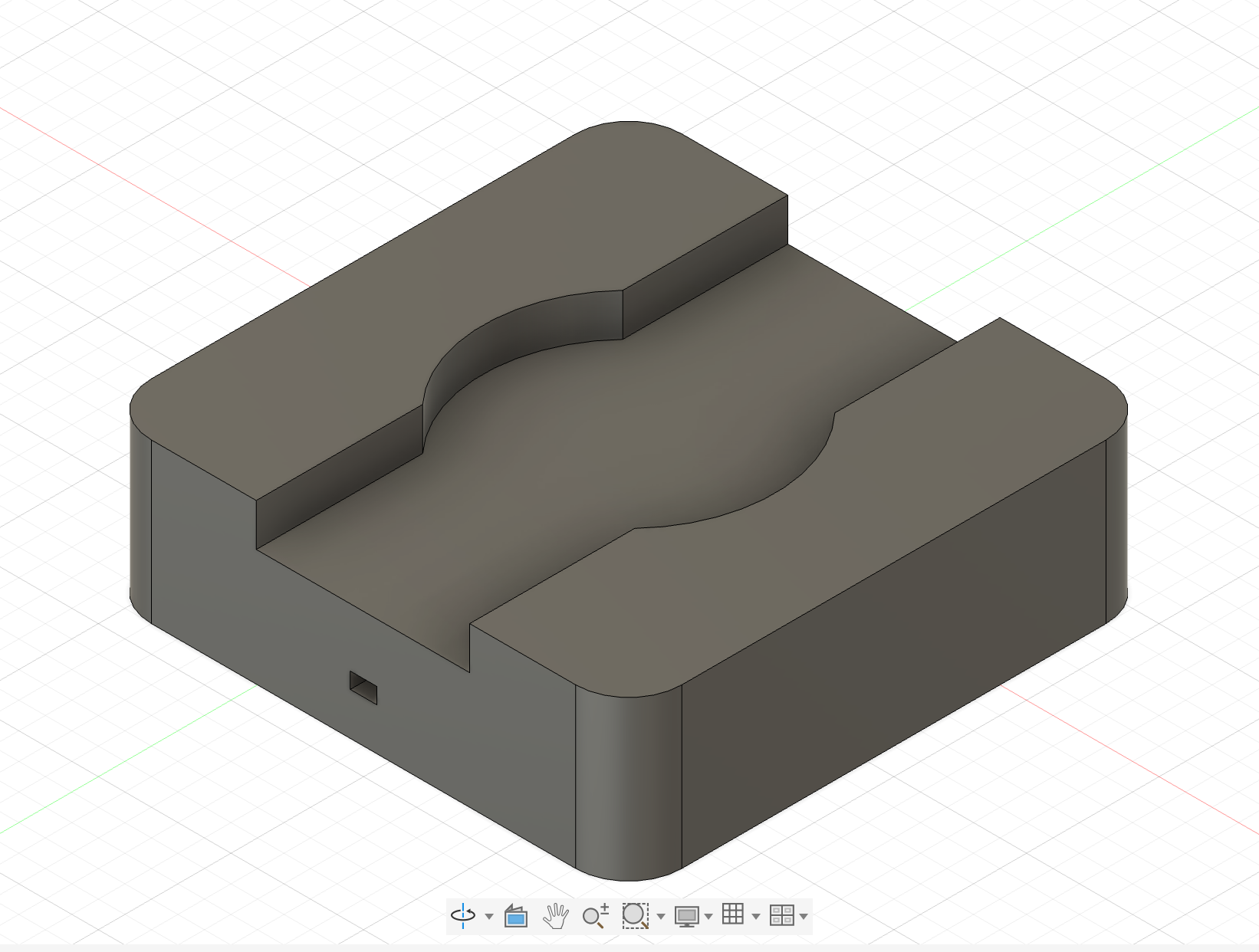
Wood Box
I also designed a cahrging box for my watch that can be milled with CNC on wood stock. I could implement a few holes for POGO charging pins to charge my watch. Since I removed the battery related components on my PCB, I didn't end up executing the CNC cut. Here is the design:
AI Model
There are many different models that I can choose from, but mainly the feature I'm looking for is realtime audio to text transcription and diarization.
Here are some of the options I look at:
- Openai Whisper + Pyanno
I also wanted a simple model that can satisfy my needs, and thankfully I found GPT-4o Transcribe Diarize, which has a straight forward API and features including audio transcription. The cost is $6 for every 1M audio token inputs, which is quite manageble for short amount of testing and demo.
Software
I used Python's flask to create a web server that takes in post request containing the raw audio files and send the data to GPT Whisper to transcribe the audio. Then the data is sent to the LLM for analysis.
I also built a small web interface for users to track all the speech analyzed.
Last Day
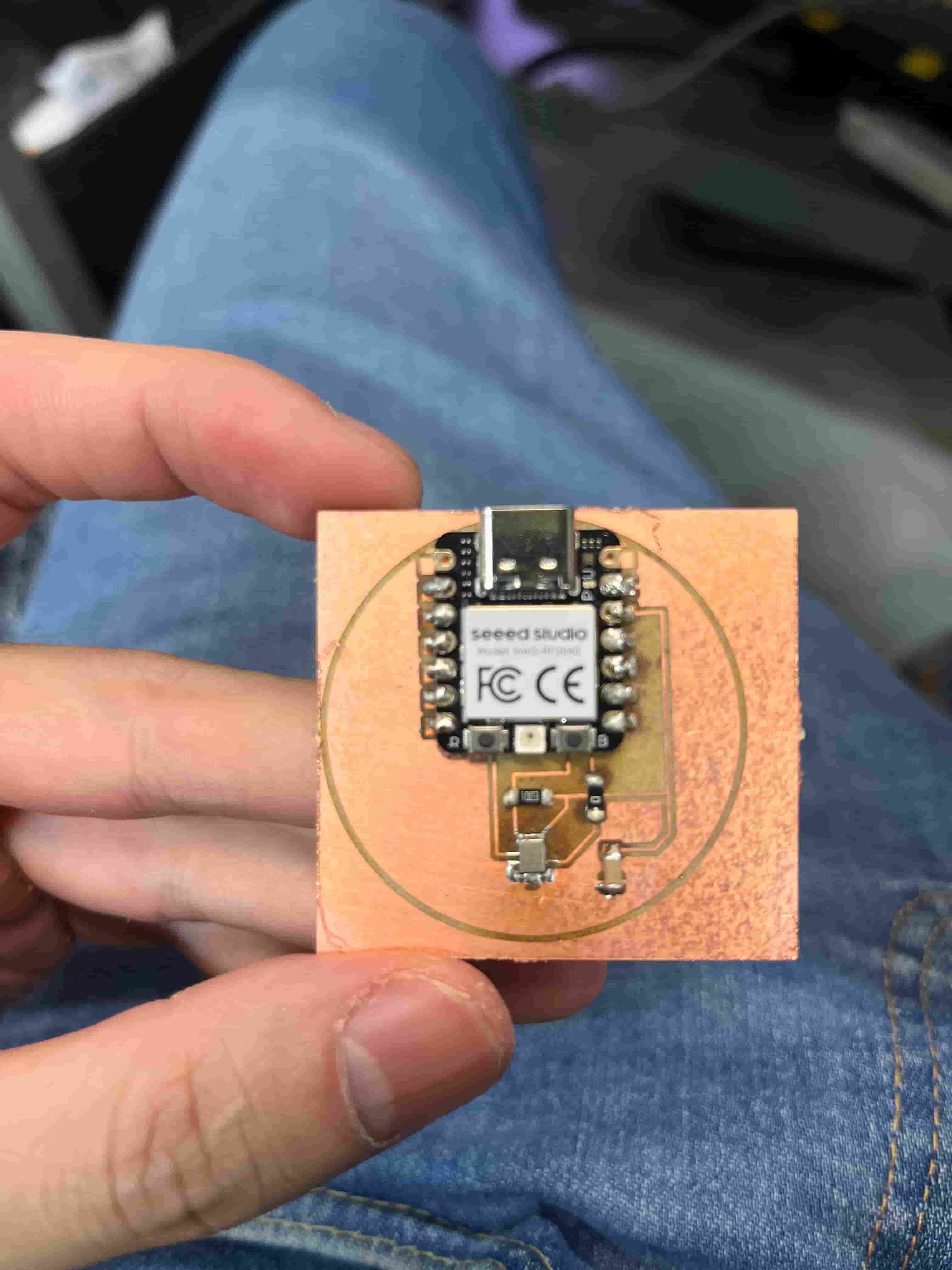
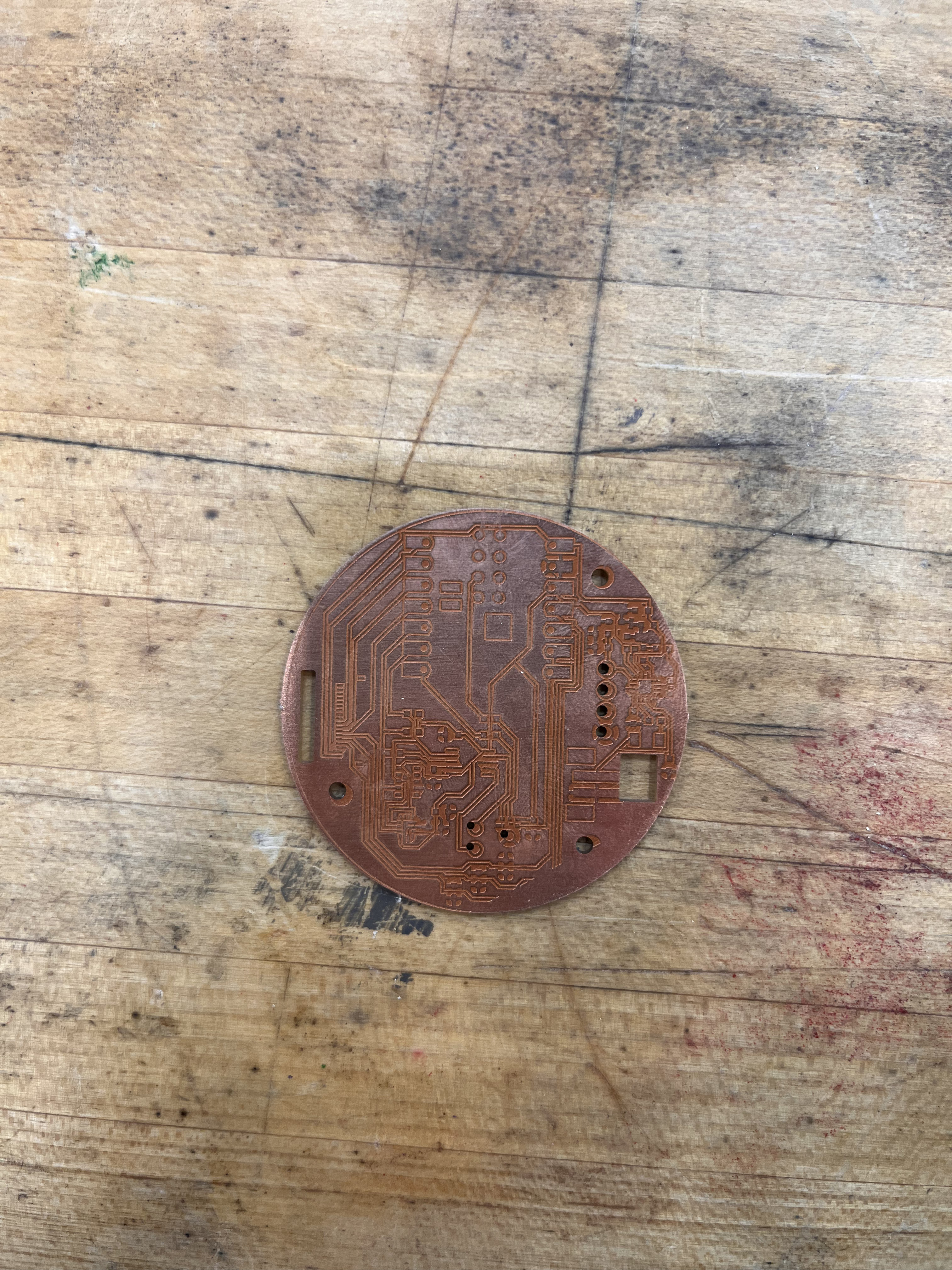
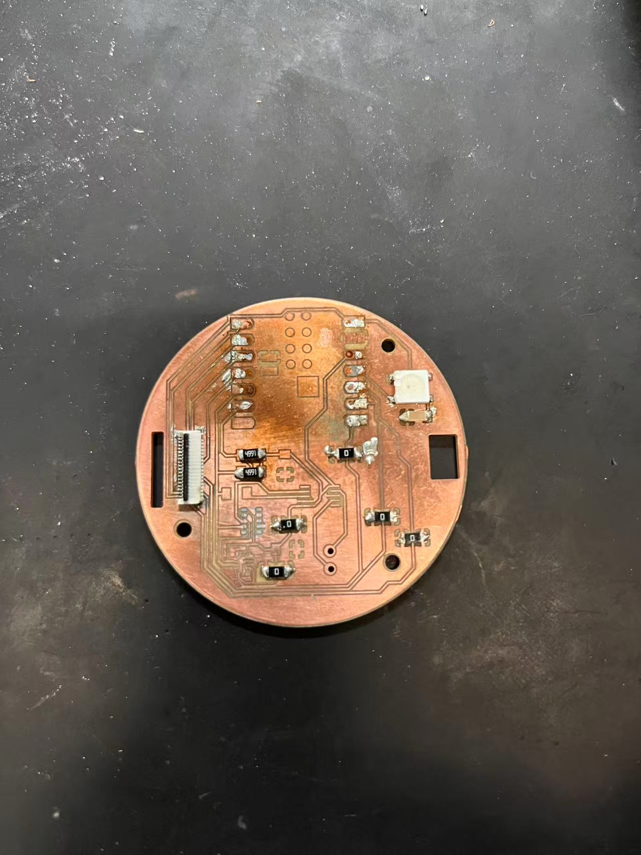
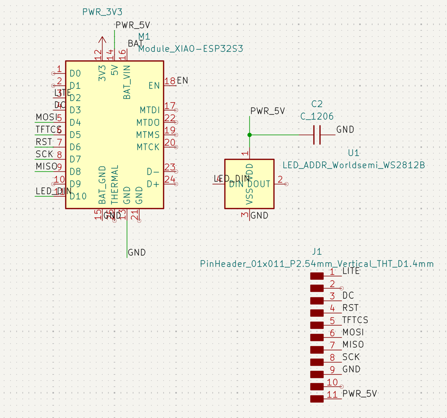
After realizing that my board is beyodn salvage, I have exactly 16 hours before the presentation. I completely reworked the design of my PCB. I decided to mill my PCB with the carvera with large traces for fast milling and easy soldering.
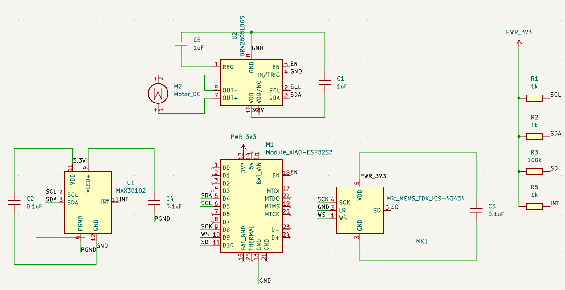
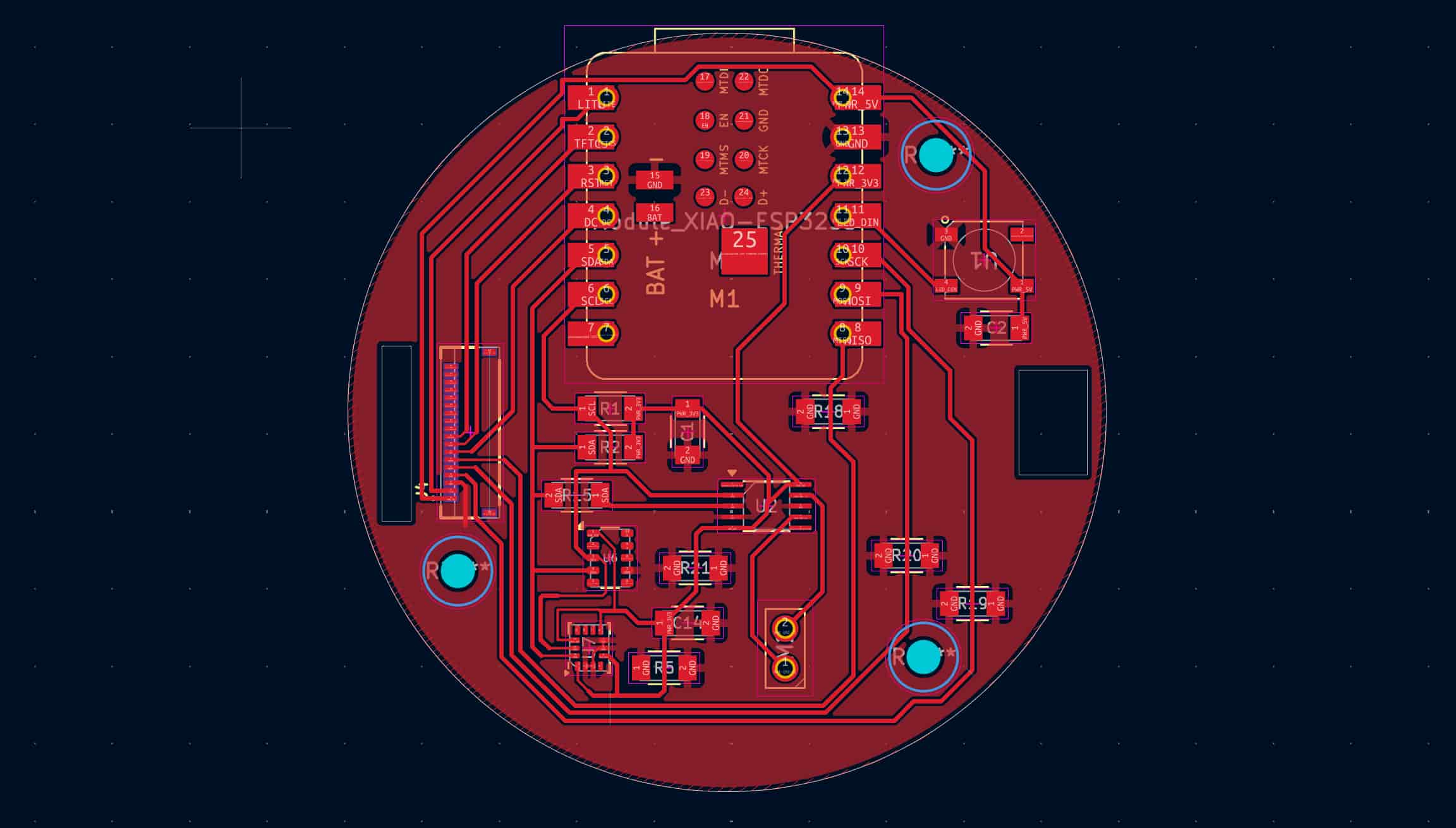
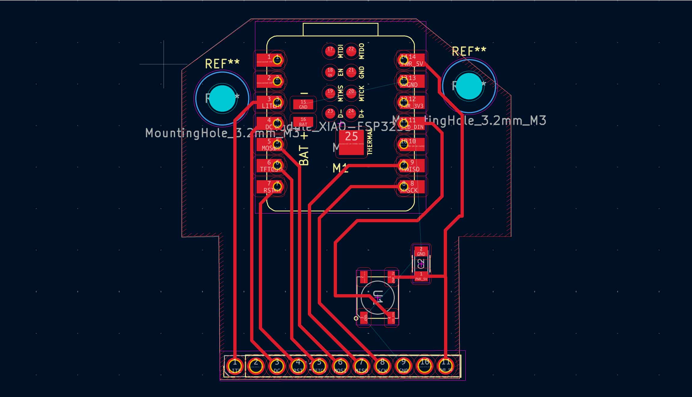
Here's the final schematic:
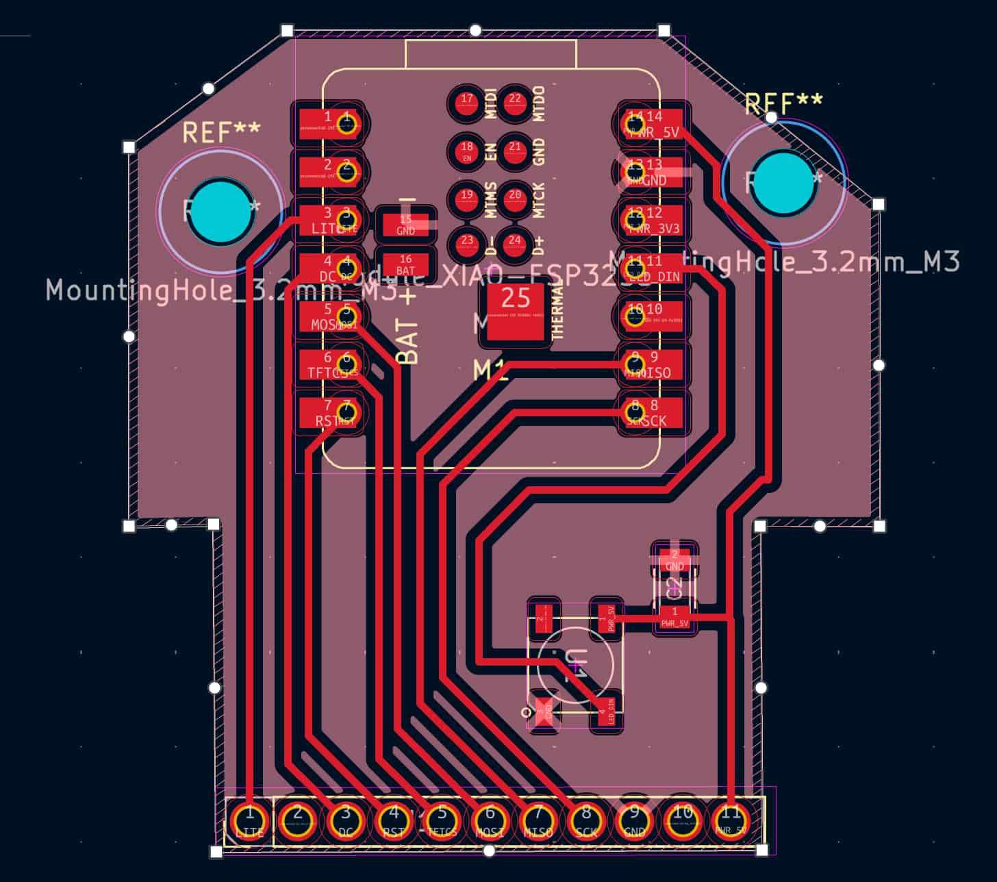
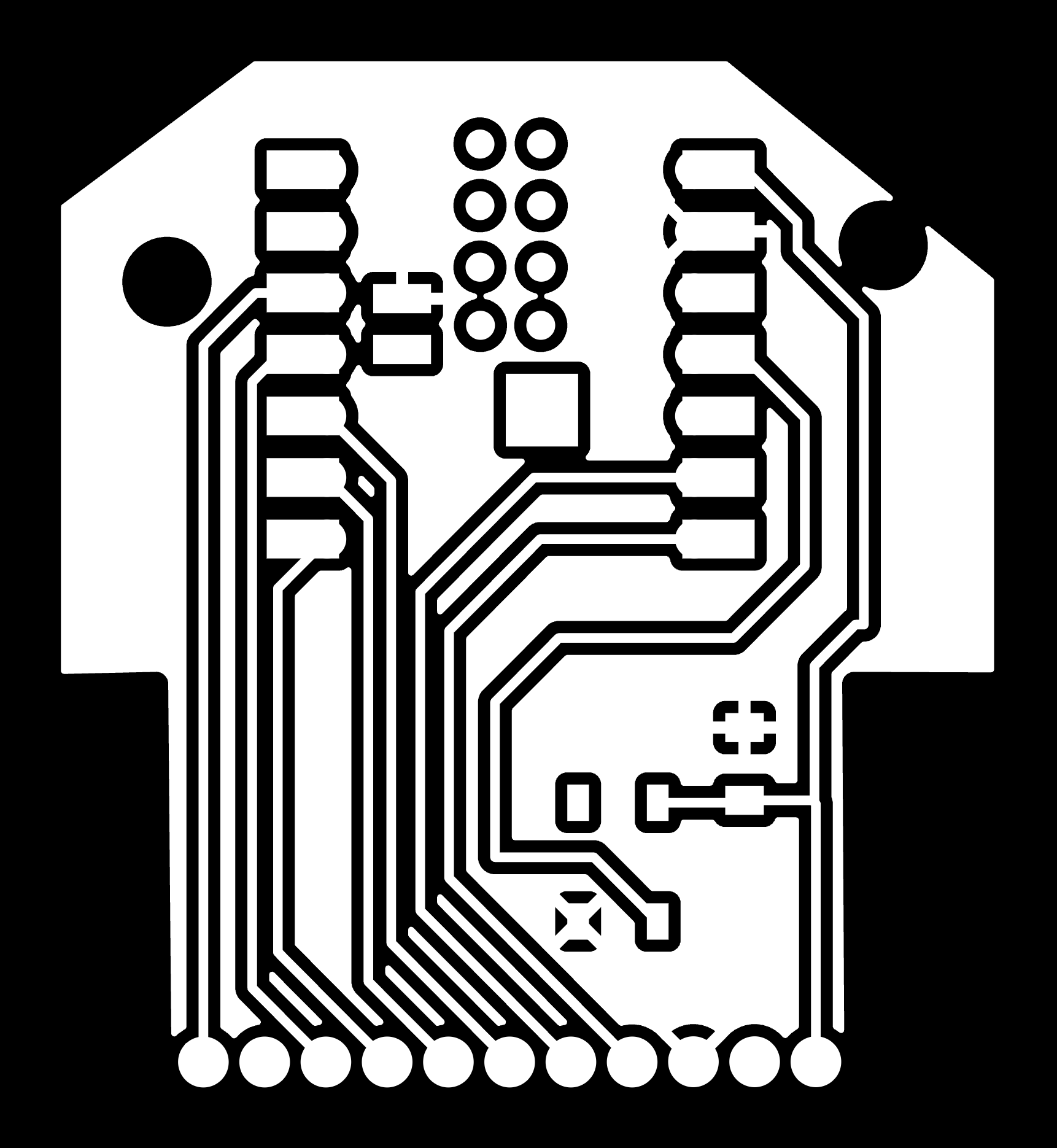
 Here's the final PCB:
 I also reworked my case and removed the spaces reserved for the battery and the linear motor.
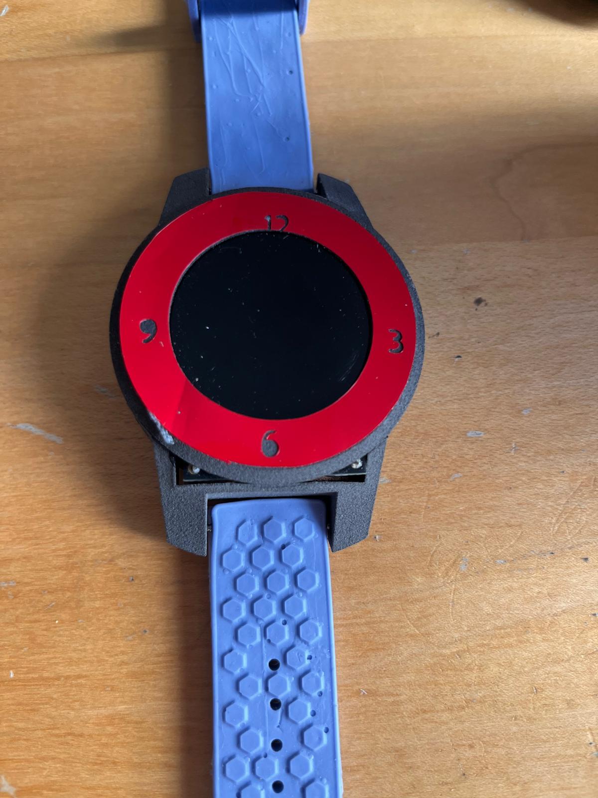
Lastly, I used the CricutMaker 3.0 vinyl cutter to make the design and cut some texts on red vinyl to add a tint of bright color for my watch bezel.
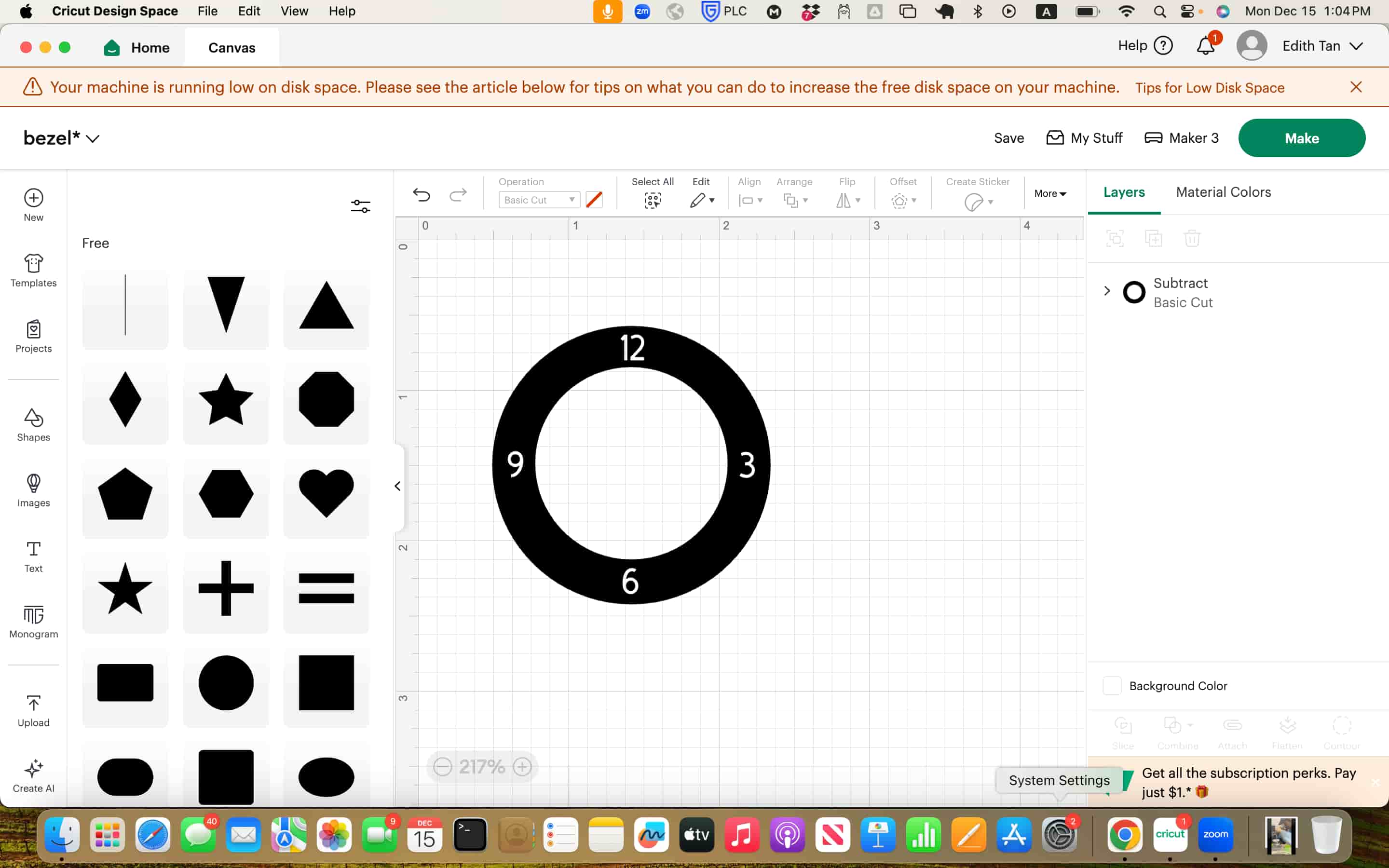
I attached the sticker onto the bezel of my watch.
Slides
What does it do?
It listens to conversations and provide live feedback through LED and screen.
Who's done what beforehand?
While there are many wearable devices for sports, lifestyle, AI assistant, not one device focuses on live conversation analysis and feedback. This is why I want to learn to build a wearable and test whether it is possible to build a hardware device that could potentially help improve people's social lives.
In terms of custom building watch, there is a cool inspiration from ZSWatch. They helped inspire me in understanding the scopes and parts needed in a smart device. However, their PCB design link is lost so you could mainly judge from images.
What did you design?
I designed the PCB, the watch case including the bezel, body, and base, a watch box, and the vinyl cutter sticker that goes on top of the watch bezel.
Materials and Components Used Cost
Many components and materials were considered, but the final device is relatively simple and straight forward.
- Adafruit 1.28" 240x240 Round TFT LCD Display with MicroSD - GC9A01A with EYESPI Connector: $17.50
- Seeed Studio XIAO ESP32-S3 Sense from inventory: Free
- WS2812B RGB LED from classmate Matti: Priceless ($
- Nylon from CBA inventory: Free
- FR1 Board from CBA shop: Free
- Adhesive Vinyl from CBA shop: Free
Parts and Systems
There are a few parts to my project. The first is the 3D printed watch case with bezel, main body, and a base. The second is the PCB incorporating the ESP32-S3 Sense, an RGB LED, and a LCD screen. The last part is the software, which included the arduino processing the audio and sending it to a web server, that uses GPT-4o Whisper to do audio transcription and GPT for conversation analysis. The embedded code then send command to the hardware for LED to light up in different colors or the screen to display the feedback test. I also have a website built with HTML showing the log of analyzed speech, which helped the users to review past conversations.
Tools and Processes
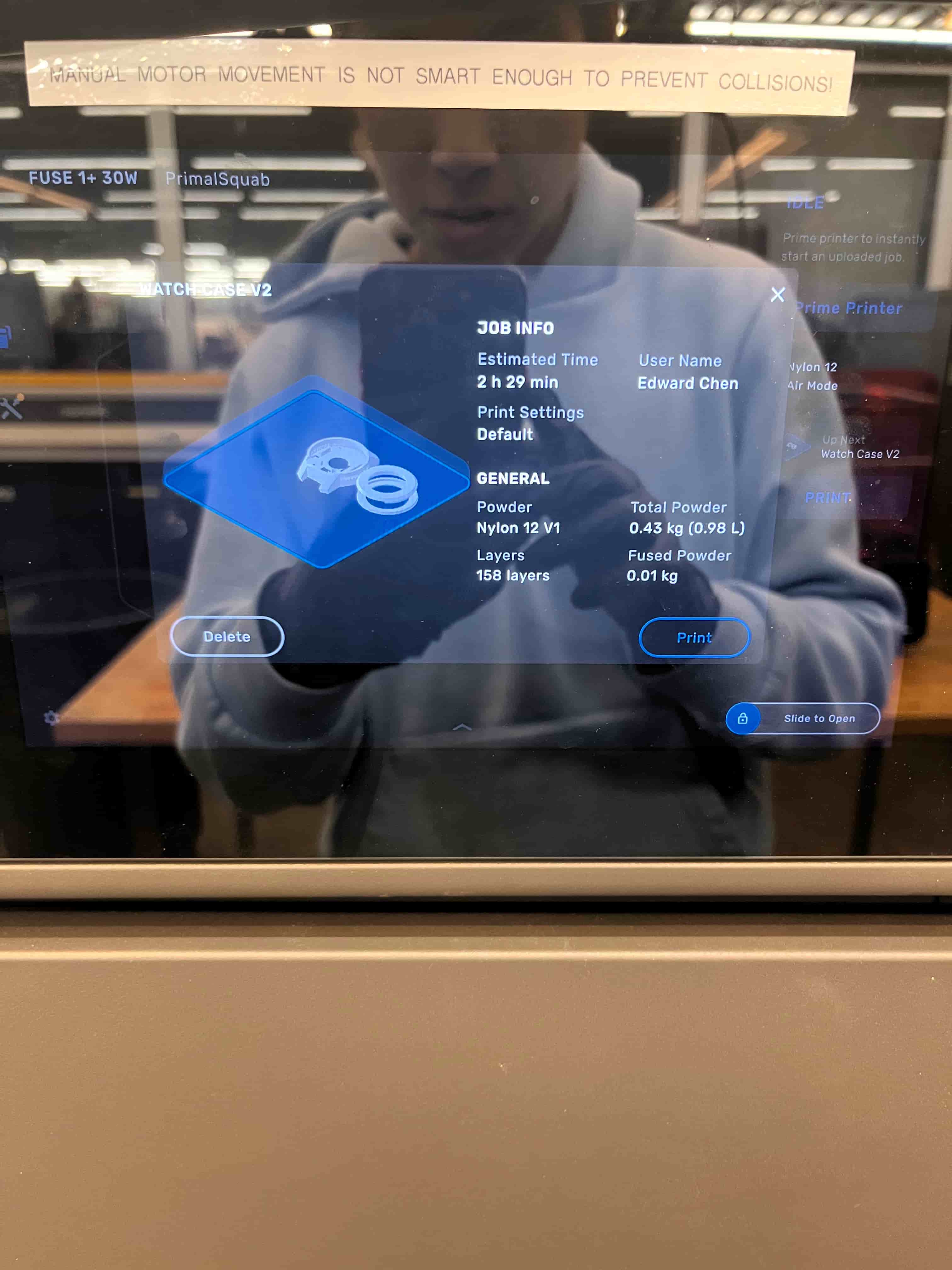
The first tool I use is the Form Fuse 1 for nylon printing my case. The Form Fuse 1 is relatively straight forward to use. Following a simple video tutorial, it was easy to learn even without any experience. I added my stl file to the PreForm application, then connected my computer to the printer to upload the print. Then, it took about 4 hours before the print is finished. Compared to the Prusa printers, the print is almost always flawless and consistent, and is able to print at very high details. For example, I was able to print very smooth threads before to screw in my base to the main case. After the print is completed, I waited for the chamber to cool down and moved the build chamber to the Fuse Sift for post-processing. I also vacuumed the printer in the mean time to help the next person using the printer. For post-processing, I use brushes to brush off the powder around my print, and then went to the sand blaster to clear off some remaining powder that is hard to remove with just brushes.
The second tool I used is the Carvera machine. First, we need to get plot our PCBs in kicad to get the traces and edge cut gerber files. Then using the gerber2img, I converted the gerber files into black and white images. Using mods CE mill 2D PCB, I only inserted the edge cut with drill holes to calculate the GCODE needed to cut the board. I then moved to using XTool Creative Space connecting to the XTool Ultra F1 Ultra. I used the traces feature on the images to get the traces. The dark color in XTool represents the engraved part. I then used XTool's laser engrave function with Fiber IR, 100% speed, 750mm/s speed, 10 passes, and 300 lines per cm to engrave the board. This allowed me to design with much smaller traces and clearances in Kicad, with the minimum trace size being 0.15mm. For the last board I cut, I just calculated the GCODE in mods using both the traces image and exterior image.
The third tool I used was Oomoo's silicone rubber mold to make the wristband for my watch. I first created Formlab's Form 4 printer to 3d print the negative mold, before pouring the casting material into the model. This casting process takes approximately 6 hours. For the pin holes, I raised the pillars higher than the box so that when pouring the cast material, they don't cover the holes and then I have to poke through the thin layer later on. I then used a dremel to drill the vertical holes for the pins used to connect the wristband to the watch.
The last tool I used was CricutMaker 3. In Cricut Design Space, I made two circles, the big circle matching the bezel size and the small circle matching the screen size. I added texts and then used the combine cut feature cut only the outer ring.
What questions were answered?
The questions answered is that wearable device can be more than just fitness trackers. It can be incorporated into more functions crucial to our lives. I believe this is a good baby step for showing how conversations can be analyzed in real time with the power of AI. Another questions answered was my ability to build small stuff. While people warned me of the challenges of building small stuff, I worked very hard to learn about using XTool to manufacture small PCB boards, using heat gun to solder small components, and tirelessly refining my design in KiCad so many components can fit in a compact space.
What worked? What didn't?
The final result worked. Audio was captured and sent to the server, before being analyzed by the LLM with feedback.
What didn't quite work was that I tried to capture exact timing of when user speaks using Root Mean Square to find out the loudness of an audio signal over time. Only RMS higher than a pre-determined threshold is captured and sent to the server. However, this is somewhat inconsistent as it sometimes captures very short period (less than 1s) of auido instead of the complete sentences. Perhaps a more intuitive way of doing it would be to just capture and send 5 second chunk of audio and have the LLM continue to compile and cut off.
What also didn't work as I documented a lot was just that I didn't get to complete my initial design of a complex and compact watch.
How was it evaluated?
I evaluated by testing few things:
I'm lenient on myself because I think the final device works functionally and is integrated nicely. But this is defintely not how I envision my end result to turn out, so I was still very sad on the last day knowing I won't be able to accomplish what I imagined starting out.
Implications
I think the implications is huge. As 1/3 of the people are introverted or shy, and the increasing use of technology is also reducing the genuine social interactions people use to have. Nowadays, people are more acquainted with the convenience of texting, which does help us reach people all around the globe. However, we might be less focused on the people around us, people who are physically present. Whether that is dating, networking, interviewing, presenting about your projects, showing your strengths, being charismatic, persuasive, and friendly is still something that can help people immensely. I hope wearable devices can be used for more use cases, such as helping people become more confident and expressive.
Other more specific use cases also exist. For example, I was listening to the Fostering America forum and listening to one of the speaker at Deloitte sharing about them using VR to help train their case agents in simulating conversing with parents and evaluating whether the children should be taken away. While these kind of training is helpful, the real life is always going to be different and unexpected things might happen. What about having this agent sitting on your wrist that could listen as the situation unfold and provide hint, adding another layer of information to help the case agents.
Video
Lessons Learned
I think one of the biggest lesson I learned in this project is about spiraling. Due to the poor project planning and over-ambitious scope, I ended up reverse spiraling: which is me reducing features and the difficulty of the project as each day closer to the deadline. In the end, I created 5 versions of the PCB, each one simpler than the version before as I learned of the difficulty of soldering small components and the time it takes to laser cut boards. As I change my PCB design, I also have to slightly modify the design of my case to fit the PCB.
In addition, I finalized and bought my parts relatively late, which slowed my design process as well. For example, I initially set on a screen. But without putting the design in PCB, I didn't know how many GPIO pins it needed. And only until I was designing later that I realize that I might not have enough GPIO pins to incorporate the touch screen. Another example is my haptic driver, which I bought around mid octorber. I only learned a few days before the deadline that the footprint I was working with in Kicad was slightly larger than the actual part. This is mainly due to me starting late on making the board and soldering. If I was diligent enough to make a simpler design and test earlier, I would have learned of this misalignment sooner.
Future Plans
As Neil had said, the class had only started when it end. I was not quite satisfied with my final outcome mainly due to a few blockers. I would love to use the help of professional workhouse to help me manufacture the PCB as well as milling metal cases. Then, I could build the charging station myself, which is an easier build as less components are needed and I can have a larger dimension for it as well. More importantly, I would want to continue exploring different features that is different from the current mainstream products, which mostly focuses on being smart, tracking sport and sleep, and AI assistant. Another thing I thought is interesting is if the wearable can track a wider variety of hobbies or habits people are pursuing. For example, reading, stop eating sweet food, learning to play guitar, and etc. Perservering is hard and stopping a bad habit is equally hard, but what if the wearable can help automatically track these things, and on the application interface users can enter into a pool with other people, where they keep their share of money only if they manage to perservere. Otherwise, the people who perservered the longest would take the money.
I also realize that I haven't explored building much mechanical components in this class. I explored the ball and socket joints and the scotch yoke mechanism but didn't really build it out. Looking at other people's final projects, such as Ryan's modular robot kit or Huanyu's rotating chair, I want to do more in learning about mechanical designs and building moving parts. Thus, I think a project I would like to try next in my personal arm would be a robot arm.
Files
- Kicad Full Features
- Kicad Final
- Fusion 360 Case
- Fusion 360 Box
- Fusion 360 Mold
- Traces Image
- Edge Image
- Server Code
- Embedded Code