This week focused on electronics design using EDA (Electronic Design Automation) tools. The assignment required us to simulate a circuit, design an embedded microcontroller system using parts from the lab inventory, and check design rules for fabrication.
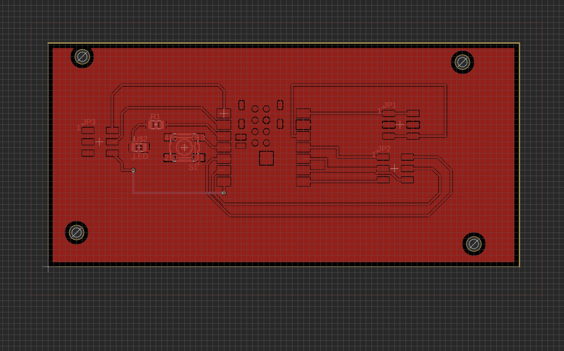
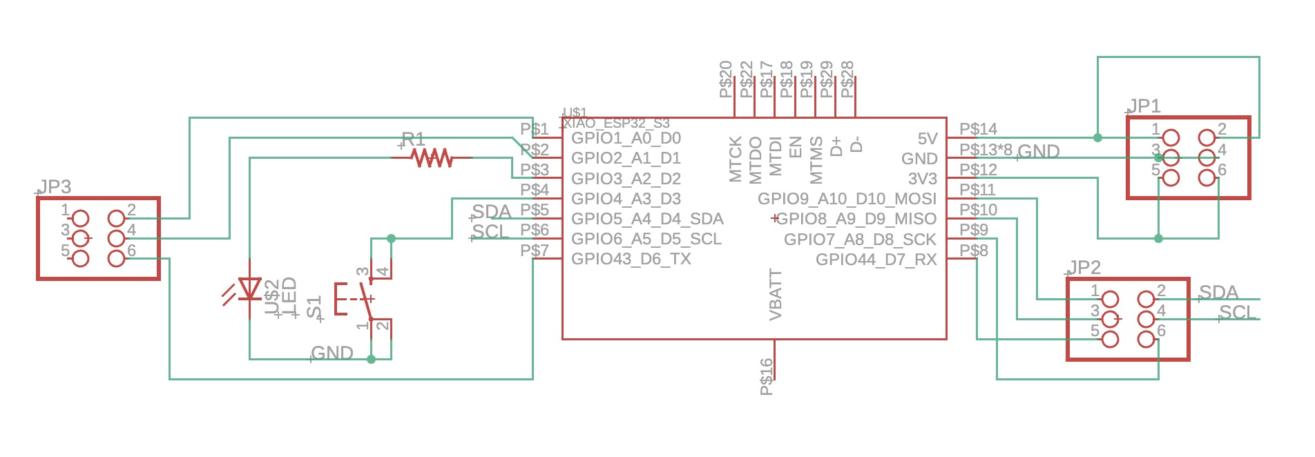
I designed a PCB for a distance sensor system using the VL53L1X Time-of-Flight sensor and an ESP32-S3 microcontroller. This board would eventually become part of my hydration monitoring system. The process involved:
Creating a schematic in Autodesk Fusion 360 Electronics
Designing the PCB layout with proper trace routing
Running Design Rule Checks (DRC) to ensure manufacturability
Checking electrical rule compliance (ERC)
Generating files for milling on the Bantam Tools machine
Pictures
Recitation
Using the OTHERMILL milling machine, you can switch out the
tool bits for different tasks:
Small tool bit: 1/64 inch (for fine details)
Large tool bit: 1/32 inch (for larger cuts)
Cut the outline after completing all the small machining for
better stability.
Tightening the tool bit when it is not fully in the shaft is
less effective; tools are stored in the red box.
The machine verifies the tool position by touching the bed
first (default moves to the top right, so boards are
left-justified on the bottom edge).
Copper boards are 1.6mm thick, the standard thickness of
copper stock (1 oz per square foot).
Safe jobs: You don't need to stay near the bed during
operation.
Engraving bits have variable cut widths based on cut depth.
No overlapping tape on the back side of the board.
Minimum trace width the machine can cut: 0.009mm.
How to Make a Double-Sided Board
Use a rivet (tiny red piece with a circle on the end) to
connect the two copper plates by smashing it into a hole.
For double-sided boards, use the fixture and locate feature:
The fixture is a U-shaped bracket you screw in to locate the
board.
Software
Using Bantam software for PCB milling.
Three types of milling: holes, outline, and traces (set the
tool for each type).
1/32 inch tool for holes and outline.
1/64 inch tool for traces.
UI Notes
Red areas on the design indicate parts the selected tool
cannot cut.
White lines in the traces visualize the path of the selected
tool.
Group Assignment Notes
Input to Bantam software: Gerber file or .brd (Fusion 360).
Input settings: Plated Through Holes, Front & Bottom Copper,
Etched Cuts.
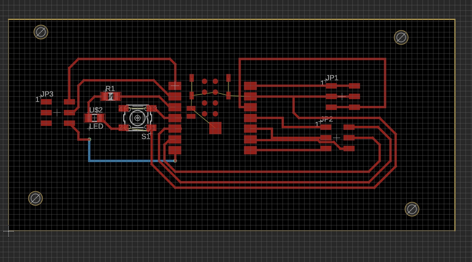
✅ No isolated copper: All pours connected to ground net
The DRC passed with no errors, confirming the design was manufacturable on our equipment.
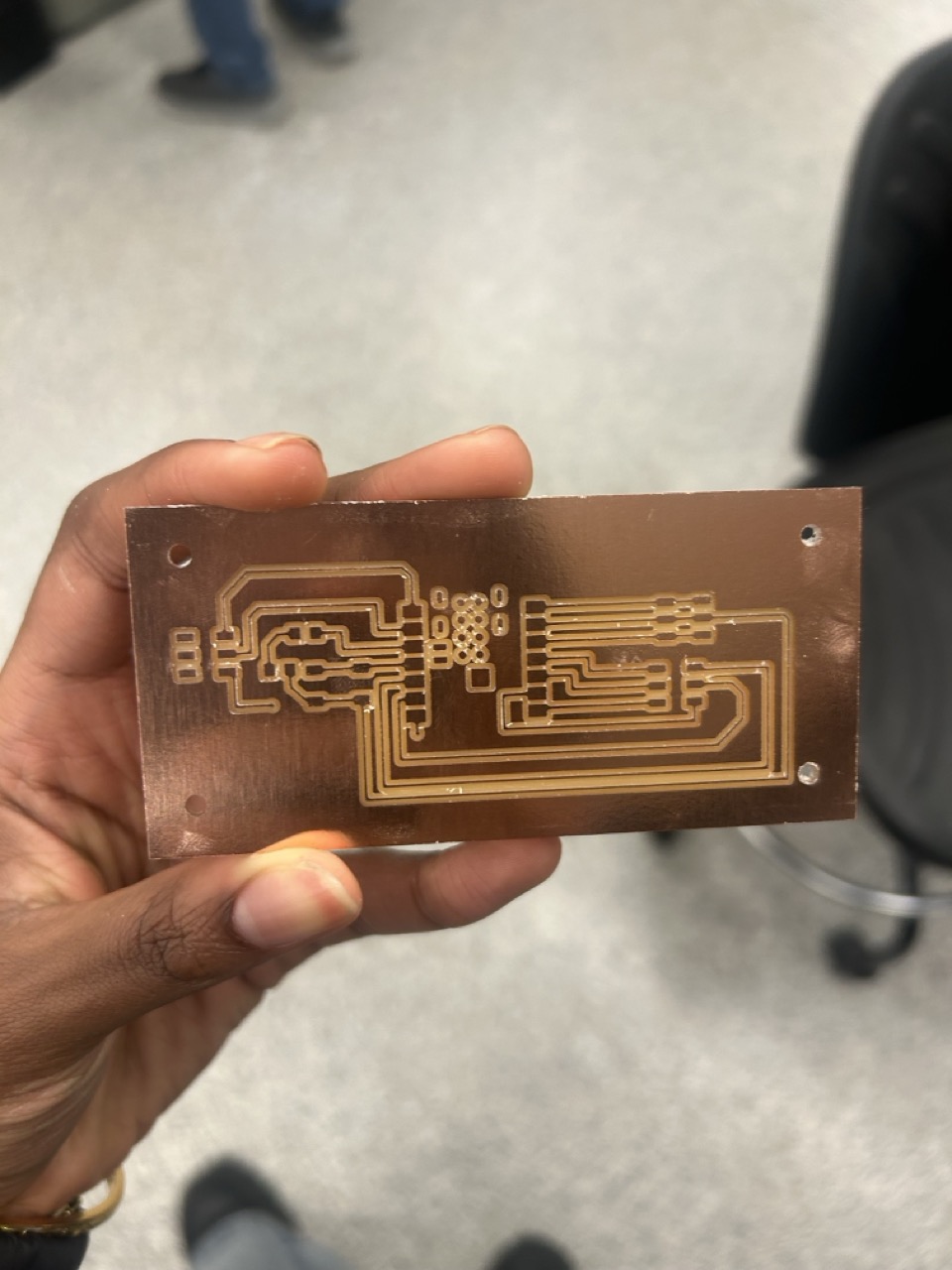
Fabrication & Assembly
I milled the board using the Bantam Tools Desktop PCB mill with a 1/64" end mill for traces and a 1/32" end mill for the outline. After milling, I soldered all components including the ESP32-S3 module, VL53L1X sensor, capacitors, resistors, and pin headers.
Finished board with all components soldered
Testing
After assembly, I programmed the ESP32-S3 via USB and tested the VL53L1X sensor using the Adafruit library. The sensor successfully measured distances from 5cm to 400cm with good accuracy. This board later became the sensing module for my final project's water bottle monitoring system.