PCB Design: DDR pads
To make progress on my final project, I wanted to prototype a PCB which will sense the DDR arrows being pressed by the user’s fingertips, and light up the LEDs when each arrow is pressed.
Collecting advice
TODO maybe: add stuff about other ways to do it eg resistive sensing using sponge
The easiest sensing mode would be something like a button or mechanical keyboard switch, but real DDR pads don’t depress when stepped on. The finger-to-copper inductive (?) sensing on the QPAD was also not totally satisfying, as I want to press the arrow pads with the tips of my fingers, which don’t always register on the touch pads as my fingernail gets in the way. So, with all of these opinions and one measly EE class worth of understanding, I went to find Quentin.
As Quentin spoke, I frantically scribed notes.
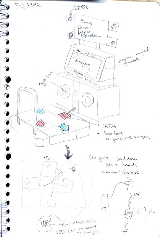
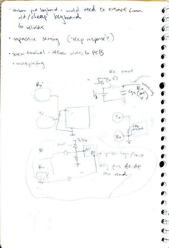
Quentin described a capacitive pressure sensor which is two conductors, separated by a layer of foam (or other insulator). One of the conductors is the transmitter (TX), and it is connected to a digital output pin on the microcontroller. The other conductor is the receiver (RX), and it is connected to two resistors (one which goes to ground, the other to the power source), as well as an analog read pin. To be honest, at this point I was feeling pretty lost.
My parents were in town for the weekend, so I was away from the shop, but luckily in close proximity to yet another talented electrical engineer: my dad. I described Quentin’s idea to him, and he described a slightly different circuit, and explained to me what the system was fundamentally doing: modulating the capacitance of a capacitor (the two conductors) and measuring the change in voltage over time as a way to get a value for how “pressed” the sensor is.
He also suggested I put the LEDs for each arrow on top of the top layer of the capacitor, instead of in the middle of the bottom pad. That way, the LED isn’t caught in the middle of the crucial “pressing” interaction, and can easily shine through the top of the outer case of the arrow pads so the user can see the light. My dad explained to me that in industry, multi-layer PCBs are the norm, and so to have a 2-layer PCB would be very doable, so that I could make a second PCB design for each arrow with an LED on one side and the transmitter conductor on the other.
I also found a Youtube video from a Microsoft-authored educational module with the same mechanism Quentin described, and did some digging and reverse engineering to figure out how this sensor is wired to the microcontroller.

Less lost, but still lost, I talked to Nikhil who explained that my dad’s circuit and Quentin’s circuit were in fact not the same thing, but based on a similar principle. I began to understand that there are several ways of doing what I am trying to achieve.
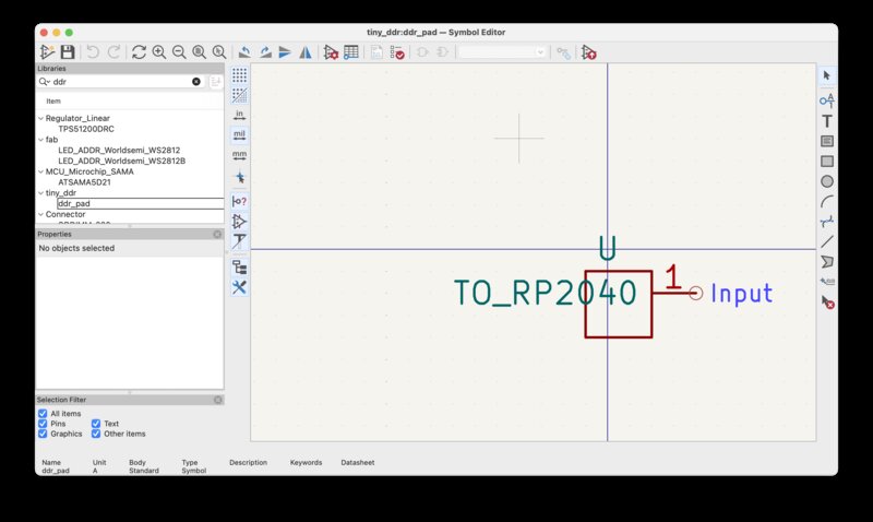
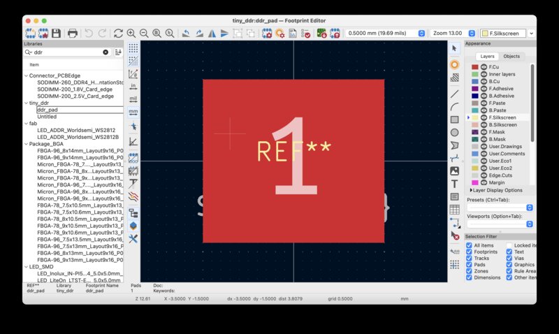
I also got some help from Sara, who showed me how to make a custom schematic component and footprint in Kicad for my copper “pads”. The process she walked me through is explained in detail in this Youtube video. Here are the pad and footprint.
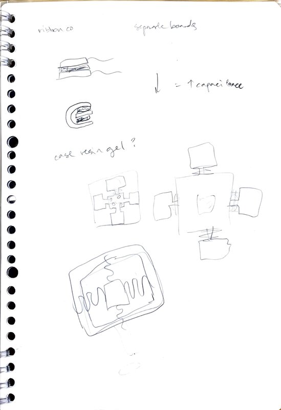
I went to visit Quentin again, to confirm my slowly solidifying understanding. He confirmed my understanding, and suggested that I use flexure to make all of the arrow pads one contiguous piece, similar to this project of Quentin’s.
How it works (I think)
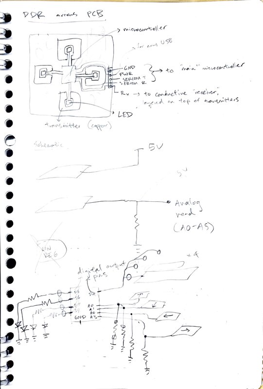
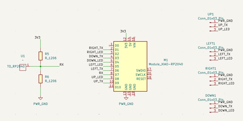
I am implementing a mutual capacitance sensor which uses step response to measure pressure. Basically, I have two conductive panels. One is connected to a digital output pin, which I will flash high, then low, similarly to Neil’s code here. This one is called the “transmitter.” The other panel is the receiver, and it is attached to an analog read pin (in addition to two resistors, one which goes to ground and the other to the power source).
Physically, I will have one large area of copper as the receiver on the same PCB as the microcontroller. Each arrow pad will have its own PCB as the transmitter. I could have chosen the reverse – to put the transmitter on the main PCB and the receiver on each of the arrow PCBs, but this configuration allows me to sauter only 2 resistors instead of 8.
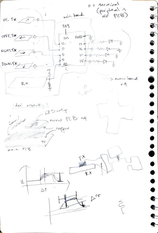
The code will set the input voltage to high and then read the voltage from the output pin. If the sensor is pressed, the capacitance will be higher, and we will see a slower rise / drop in voltage when the input pin changes its voltage, so this initial reading will be higher. For added sensitivity we will subsequently set the input voltage low, and then read again. Our output value will be the difference between the two readings, so that it will be higher when the sensor is pressed and lower when the sensor is unpressed. I’ll set some threshold to turn this value into “pressed” or “unpressed.”
Simulation
Here’s a simulation of how one of the pads works. The bottom left plot is the input voltage (which is just cycling high and low) and the on the right is the output voltage on the other side of the capacitor. The two conductive plates serve as the capacitor. As the capacitance changes, the voltage rises and falls at different rates.
The demo is live at this link; here’s a video:
V0: all in one!
My initial draft of the schematic had everything on one schematic:
![]()
However, Quentin recommended that I put my second PCB into its own KiCAD project.
V1: PCB sandwich
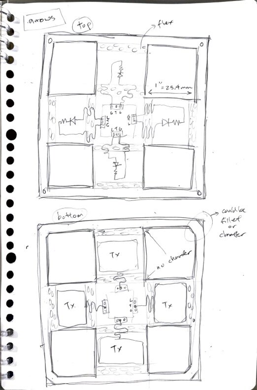
Here are some sketches I did of how the schematic should be split between the base and the arrow board, and how the traces on the base and arrow pieces should be laid out.
![]()
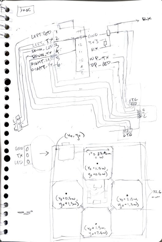
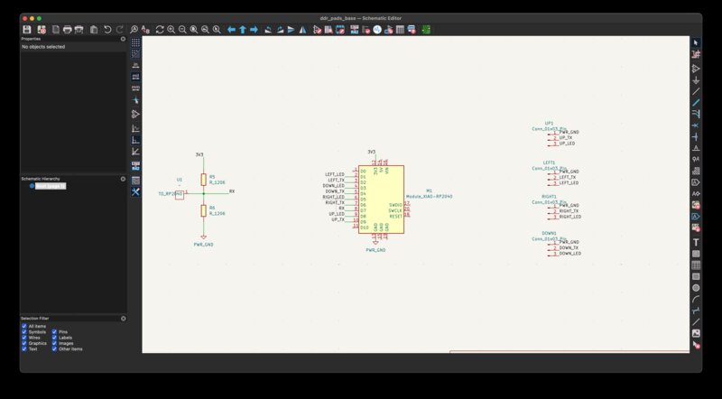
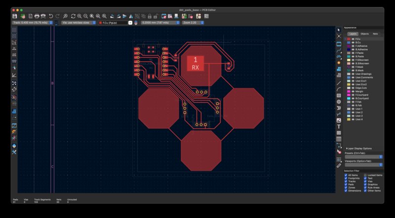
Base board
I made a new schematic for just the base, and added through hole headers to each arrow board which have a pin to ground, a pin to the digital output pin for controlling the LED, and a pin to the transmitting side of the “capacitor” (one of the two conductive plates).
I got an error that the connection headers had no footprints assigned, so I had to manually assign a footprint to the schematic element.

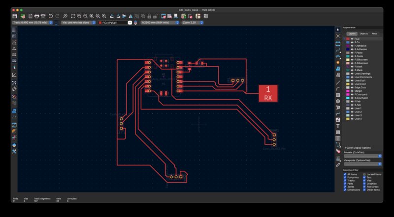
After I made the schematic I laid out a version of the circuit without the board layout itself just to get a first pass at the routing. I thought this would save me some time once I added in the edge cuts and other physical constraints, but I ultimately had to re-lay out the entire thing anyways.
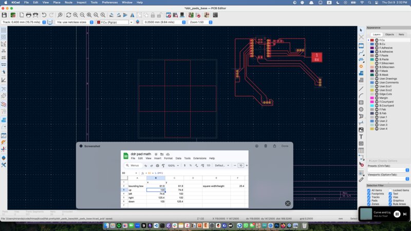
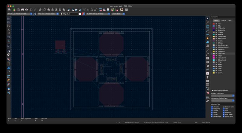
To layout the arrows, I assumed a division of a 3” square into 9 equal cells of 1” width and height. I made a small spreadsheet to calculate the midpoints of the square in such a grid and used them to parametrically layout the square pads on my board (right click the shape, Properties > By Center and Size) so that they would all be the right size and alignment:
After chamfering the shapes (right click > Shape Modification > Chamfer Lines), I drew zones over their edges and filled them to make the copper pads for the receiving side of the capacitor. I routed the traces as cleanly as I could, switching pins around on the schematic to make things easier, and ended up with this layout:
And, my final schematic:
Arrows board
For the board with the directional arrows, I first duplicated the Kicad project from the base board so I could get those tediously-positioned squares in the right place.
To implement the flexure, I merged a rectangle with two circles, like this:
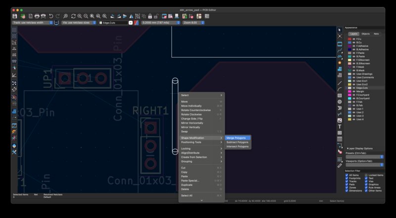
I sized the slot rectangles to be 0.8mm wide and 10mm long. After I made one slot, I duplicated it many times and positioned it roughly in the pattern of a basic flexure. I made two rows of flexure and then positioned them where I wanted them on the board.
I then merged them with the negative space squares so that the unnecessary line segments were gone and I was left with one nice clean edge cut file.
I then laid out the top of each arrow pad, which has the LED + resistor so that when the user presses an arrow pad, the LED illuminates without interfering with the mutual capacitance reading. I put the LED in the middle of the pad, “pointing” outwards, because conceptually I was thinking of it as “pointing” in the same direction as the arrow. The resistor is perpendicular, closer to the flexure, to be less in the way.
![]()
I then plotted out the conductive zones on the back side of the arrow board. My first version had simple rectangular zones, like this:
![]()
Worried that they would touch at the corners, I chamfered the zones similarly to how I’d chamfered the zones on the base board, so that the back ultimately looked like this:
However, at about this point in time I ran into Quentin and we had a conversation about how it would be easiest for this prototype to just use copper tape instead of making a double sided board for the arrows.
Here is the final schematic for my arrow board, with basically just a pin header and an LED + resistor combo for each directional arrow:
![]()
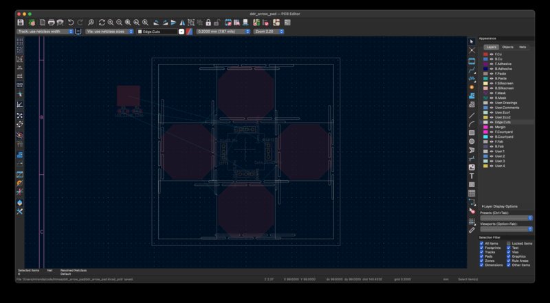
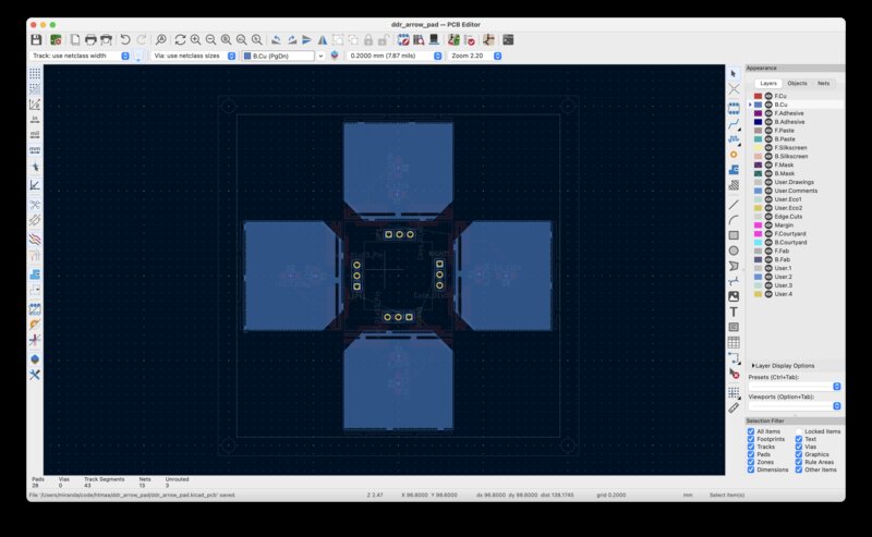
And here is my final layout:
![]()