⚙️ WEEK 5: ELECTRONICS DESIGN
Circuit design and PCB layout. Building the nervous system of machines.
Electronics Design Documentation
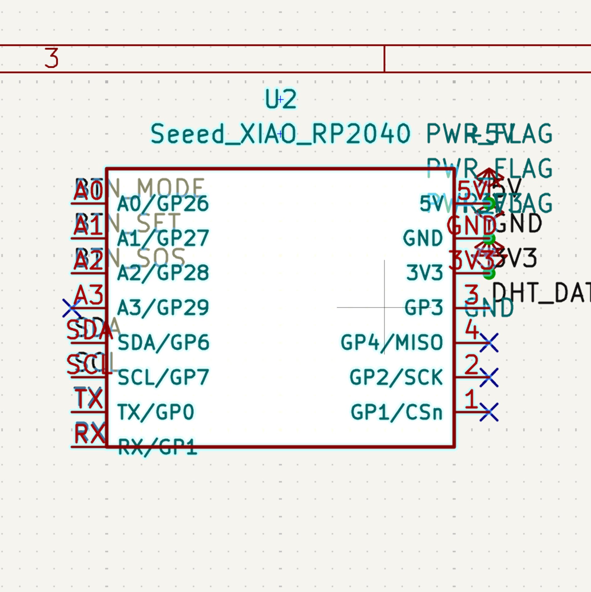
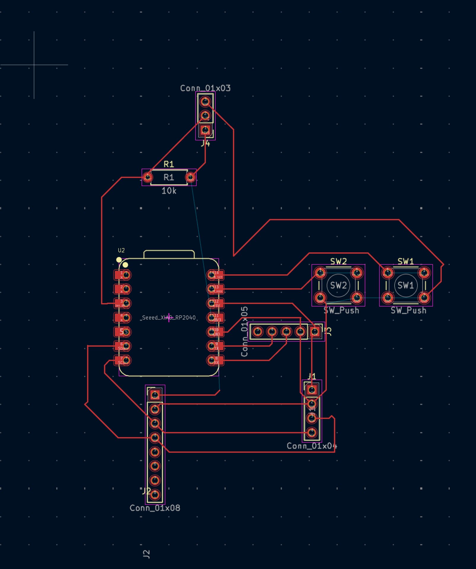
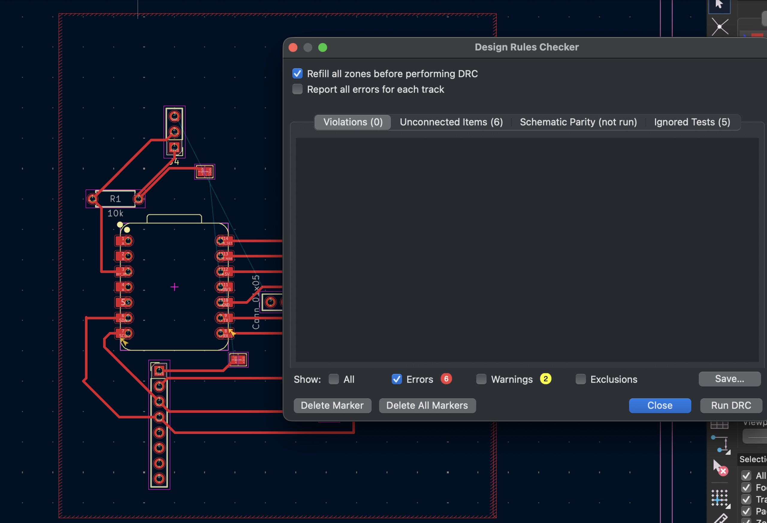
Custom PCB design for the survival device using KiCad. This week focused on schematic design, footprint creation, and PCB layout with proper design rules for the Modela mill.
Documentation & Media
Design files, renderings, and PCB layout documentation
.jpg)
PCB Layer Visualization
Interactive Gerber file viewer for PCB copper and edge layers
Copper Layer (B_Cu)
PCB trace routing for the survival device
Edge Cuts
PCB board outline and cutout paths
Design Files & Resources
KiCad project files and Gerber outputs for PCB manufacturing
Gerber Files (Manufacturing)
Survival Device-B_Cu.gbr
⬇ Download
PCB copper layer (traces)
Survival Device-Edge_Cuts.gbr
⬇ Download
PCB edge cuts (outline)
KiCad Project Files
Survival Device.kicad_pcb
⬇ Download
PCB layout file (KiCad native format)
Survival Device.kicad_sch
⬇ Download
Schematic file (KiCad native format)