Design an embedded microcontroller system using an EDA tool.
Check its design rules for fabrication and simulate operation.
Use the lab test equipment to observe microcontroller operation.
Tools
KiCad EDA
Component Search Engine
Wokwi Simulator
Multimeter
Oscilloscope
Regulated power supply
Individual Assignment
This week assignment was focused on designing a PCB that hopefully relates to the final project. I have used KiCad before in a past electronics class, so I felt somewhat familiar with the tool. I decided to focus on that laser mosquito system this week for a potential final project, since I think it would require the most advanced electronics and force me to learn the most. The basic system includes a LiDAR sensor that detects the mosquito location, a galvanometer-directed laser that shoots at the bug, and a radar wave that locates big objects (like people and pets) for safety. Power would be supplied either via outlet or a rechargeable power bank, with an internal motor that rotates the mirror position for accurate laser targeting. I also want to add a light above the camera, similar to an angler fish, to attract the mosquitos for extra efficiency. From the class inventory available, we could choose components and model our circuit board around them. The project uses the 1206 package size for SMD components, which are small enough to not clutter a board but large enough to solder reliably by hand.
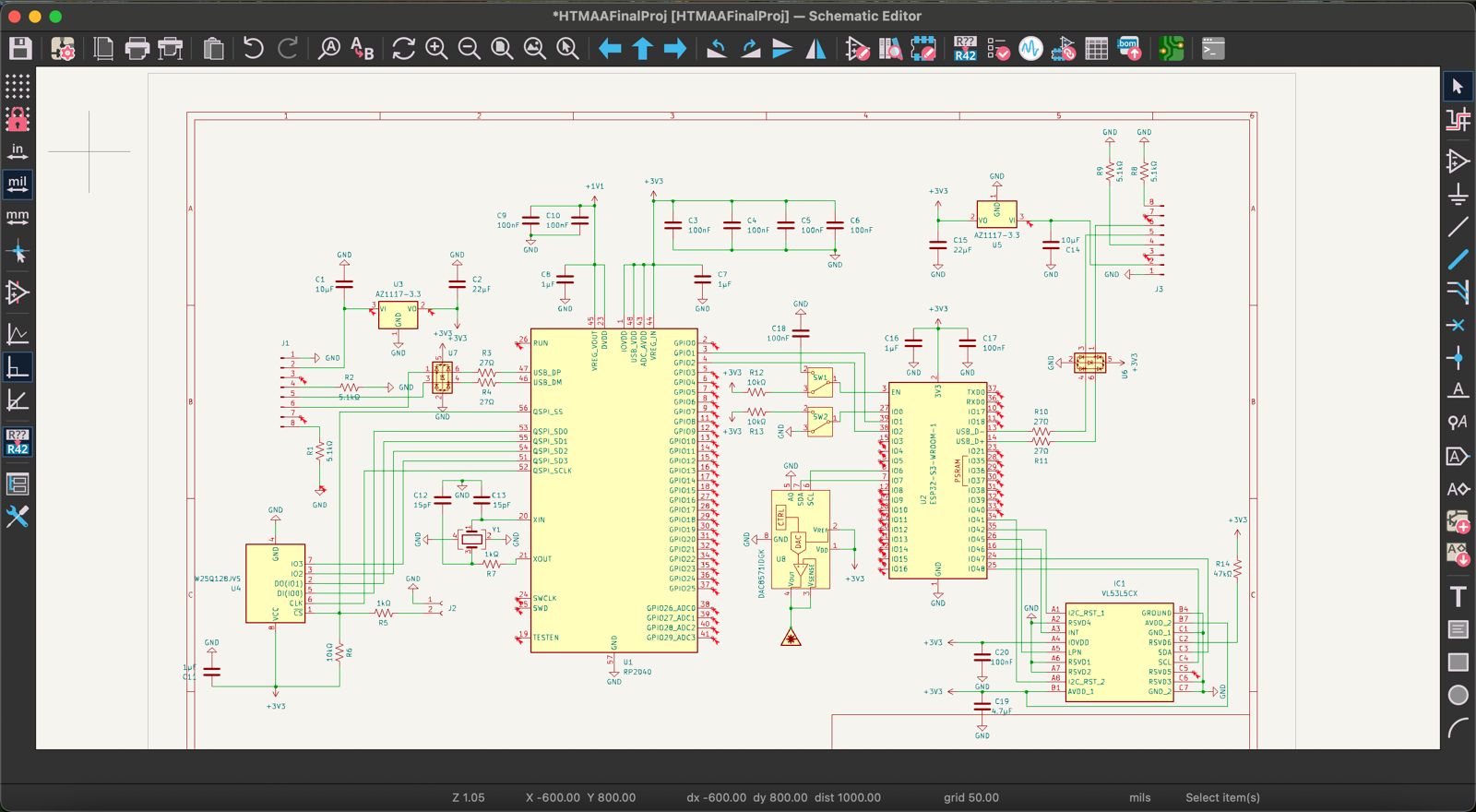
Schematic
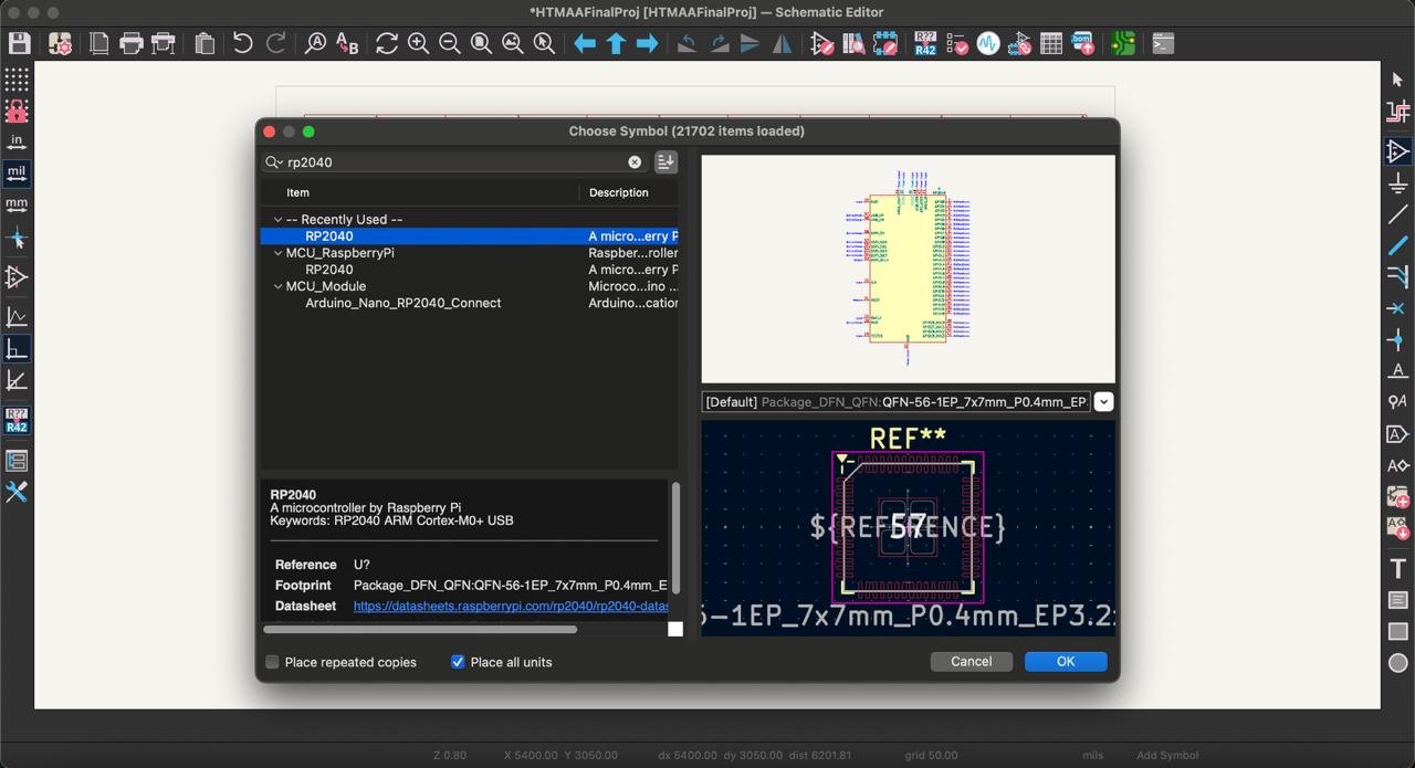
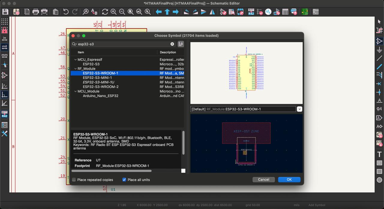
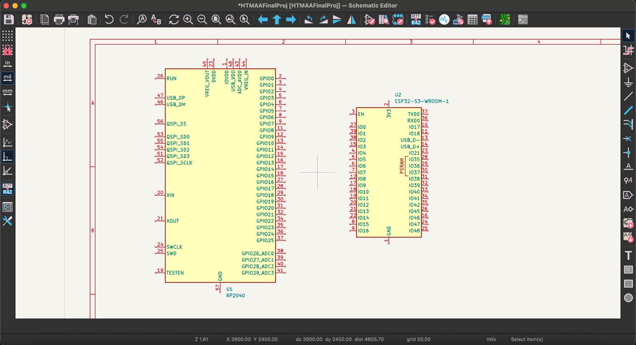
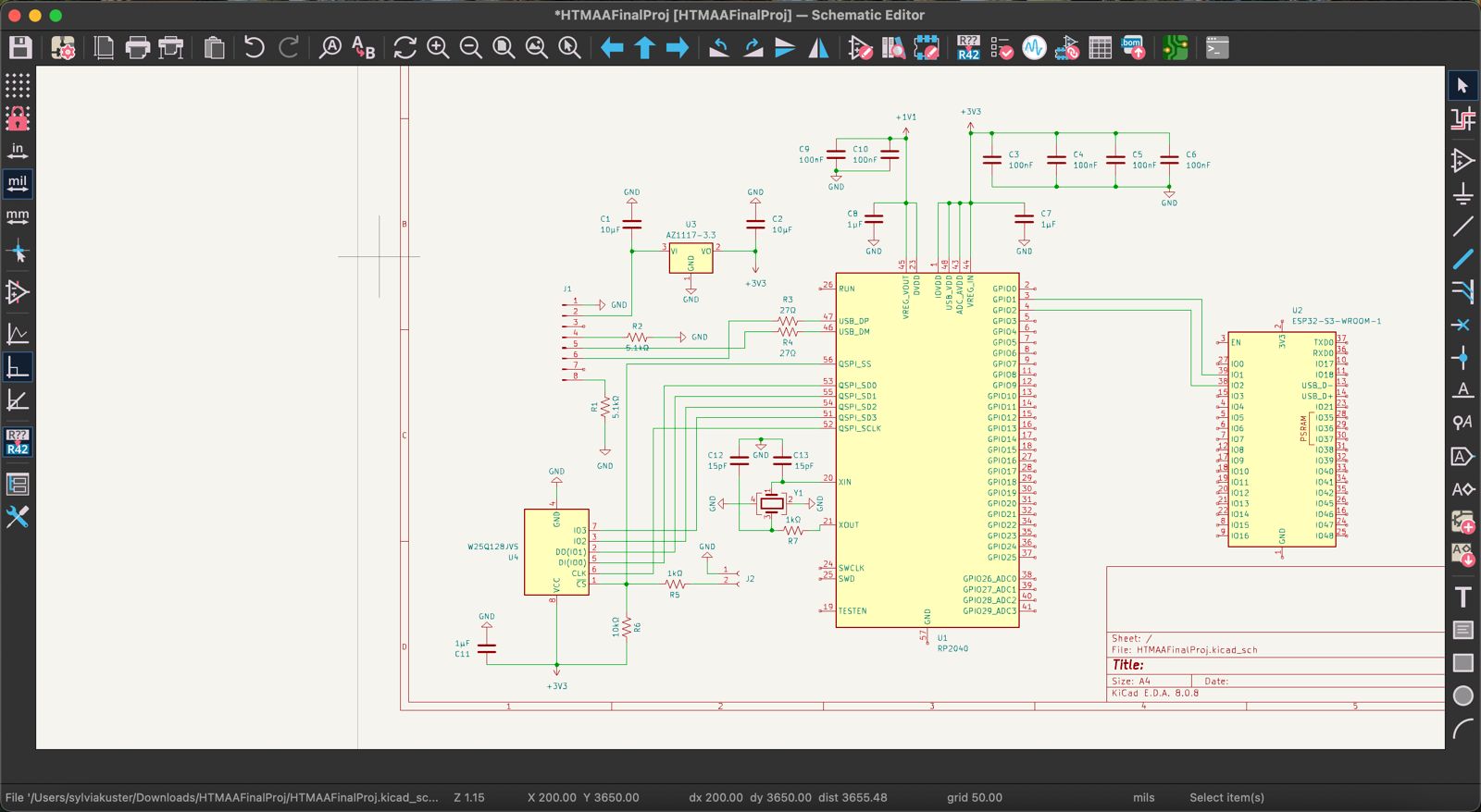
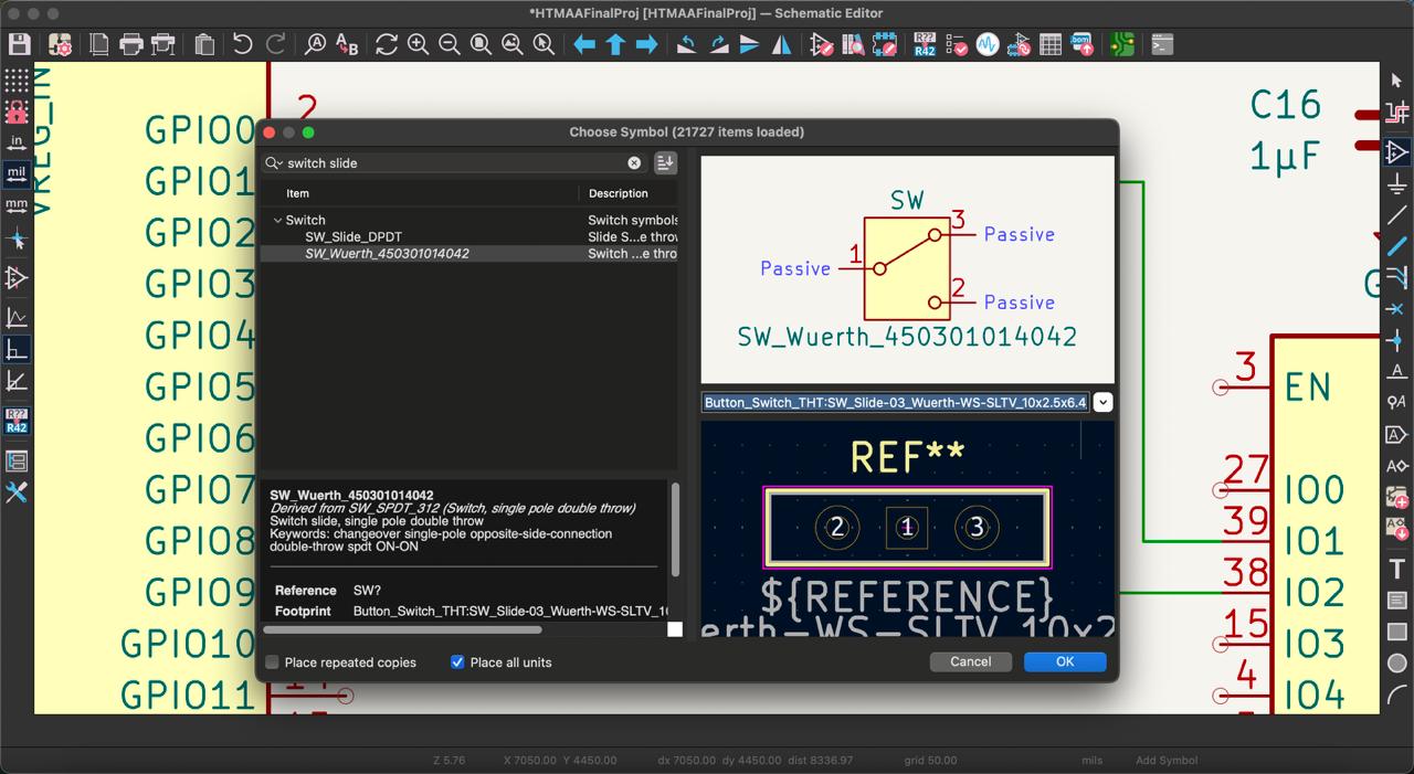
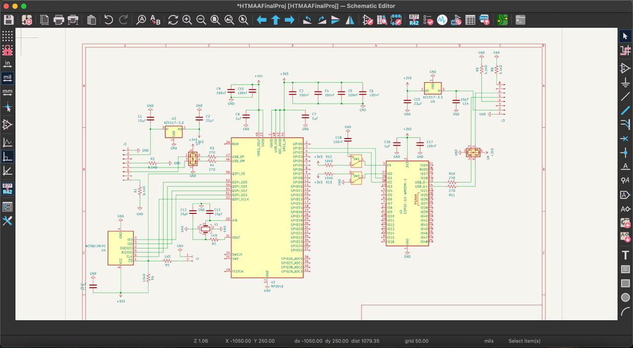
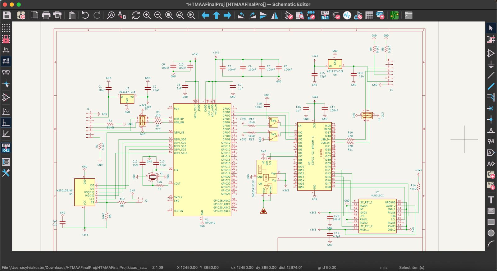
For the MCU, I decided to pair the XIAO RP2040 (QFN package) and the ESP32S3 (WROOM-1 package) together. I saw many examples online of laser DIY projects combining the two to handle parallel tasks, essentially resembling a make-your-own Raspberry Pi Pico W board. The low-latency requirement for my machine would need powerful scanning and laser logic to accurately track rapid mosquito movements (~1m/s). I opened a new project in KiCad and started on the Schematic page, where symbols are added. I pressed the A button to add the MCU components and narrowed down their Package for when I will switch to the PCB Editor.
RP2040ESP32S3MCU Schematic
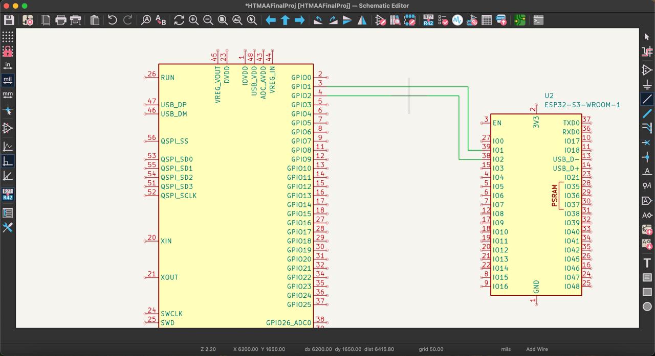
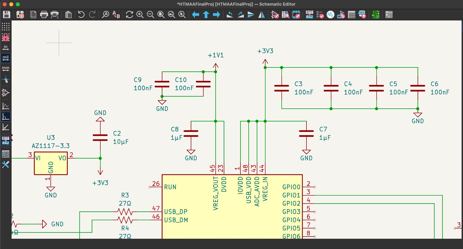
The two MCUs have multiple communication protocols to choose from, including SPI, I2C, and UART. After researching online, I decided to try the UART protocol for the project because it seems to be the simplest: no complex address schemes and only two wires: 1 to receive data and 1 to send data (and a common ground). The connections on the schematic are the RP2040 GPIO1 <-> ESP32 IO1, and the RP2040 GPIO2 <-> ESP32 IO2. Almost any RP2040 GPIO pins connected to any ESP32 IO pins would work; they both operate at 3.3V logic, so just a short connecting trace with no additional hardware is needed. I used the W keyboard shortcut to draw logical wire connections between the two boards. I then used the helpful RP2040 datasheet to guide me on what peripheral components (resistors, capacitors, switches, etc) were needed to operate and program the board. Starting with power, the board needed 3.3V for the I/O and 1.1V for the digital core, but thankfully there is already an internal low-dropout regulator (LDO) in the device (so we don't have to build one).
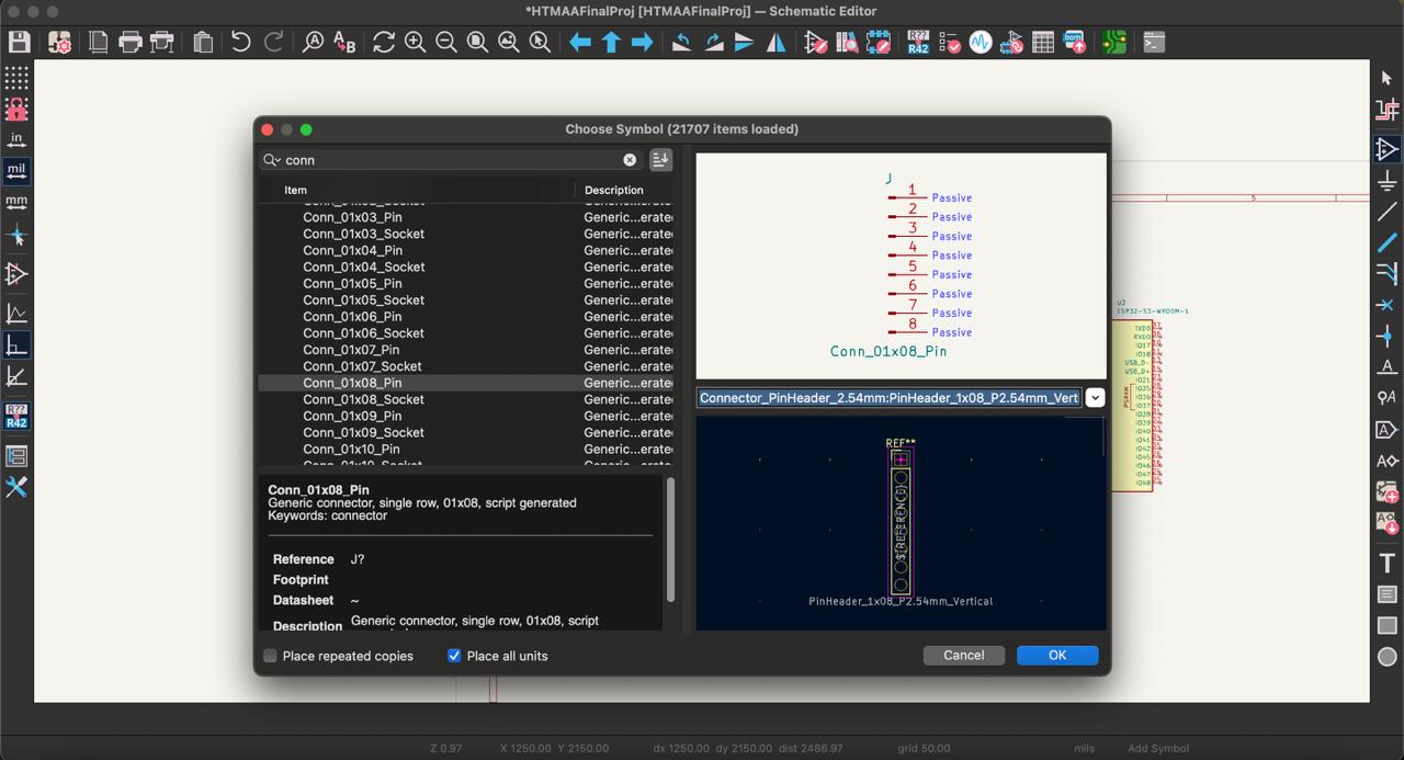
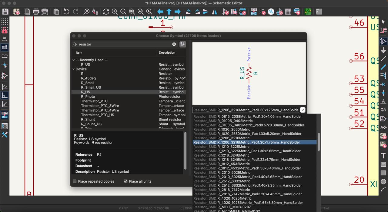
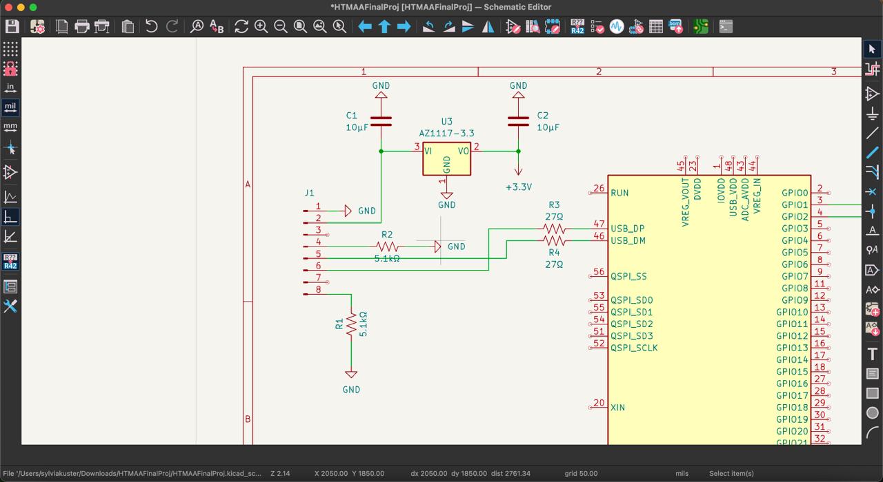
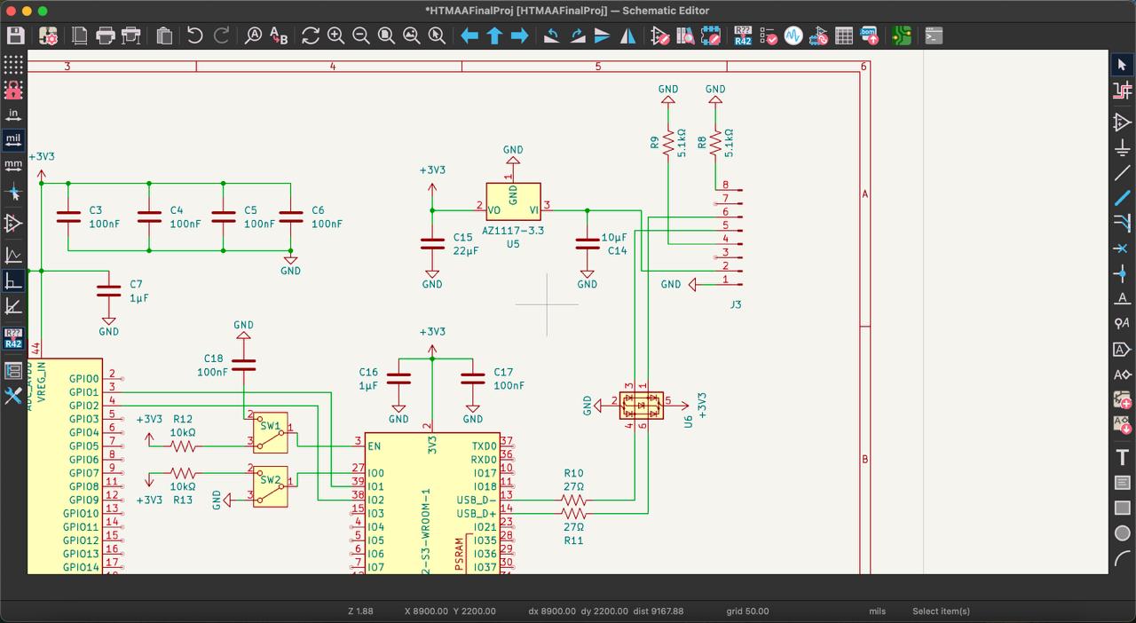
I decided on a USB-C input power connection with a 5V VBUS pin. Looking at the class inventory, there is a Adafruit USB-C breakout board which I represented in the schematic as an 8-pin header. The CC pins on the board each need a 5.1kΩ resistor to ground, as we do not care about cable orientation. The SBU pins can be left untouched, and the D+ / D- pins have corresponding pins on the RP2040 for connection (which require 27Ω resistor for impedance close to the chip). This leaves the GND pin (connected to ground), and the VBUS pin (voltage regulator system required later).
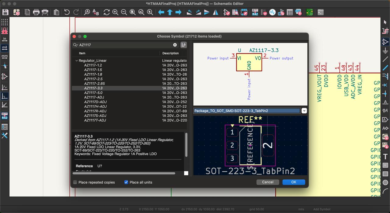
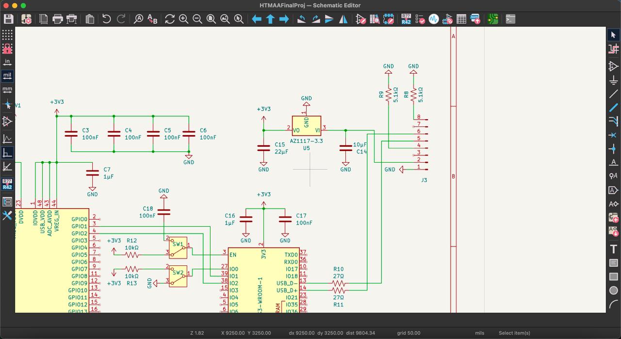
I connected the USB-C board pins and got started on the voltage regulator. The USB-C VBUS pin outputs 5V power, but the RP2040 uses 3.3V which requires a voltage step-down regulator. Following the datasheet, I added a 10μF capacitor at the input and output, along with a AZ1117IH voltage regulator. Now we have to make a decoupling capacitor circuit to filter out power supply noise and give a local supply of charge that the RP2040 pins can use at short notice. The datasheet recommends one 100nF capacitor per power pin placed as close as possible.
AZ1117IH Voltage RegulatorUSB-C Power SystemDecoupling Capacitors
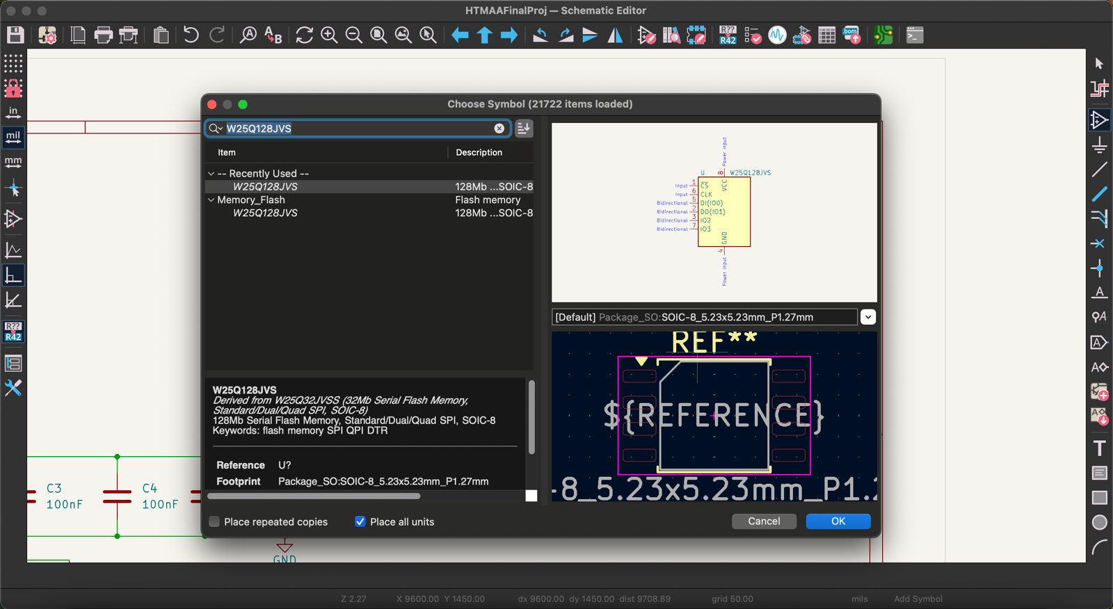
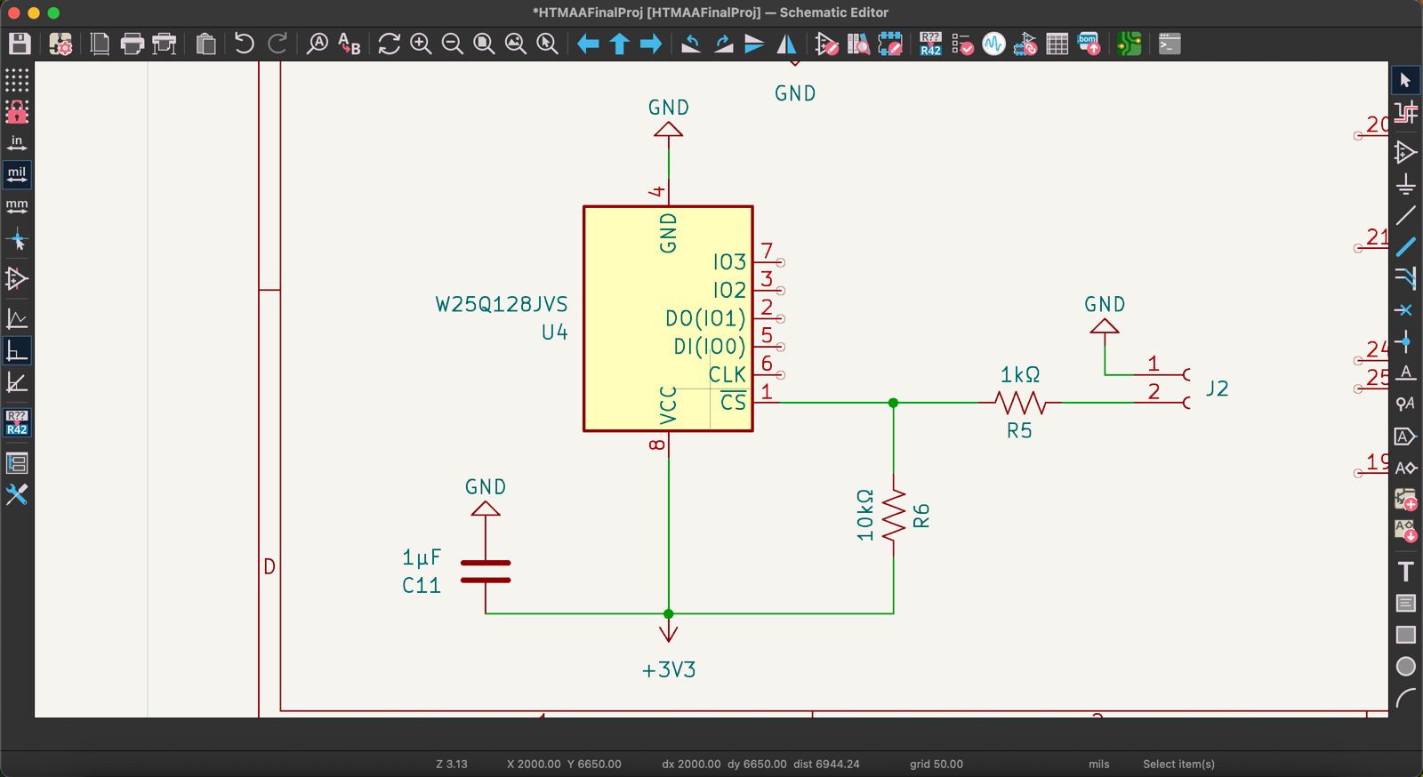
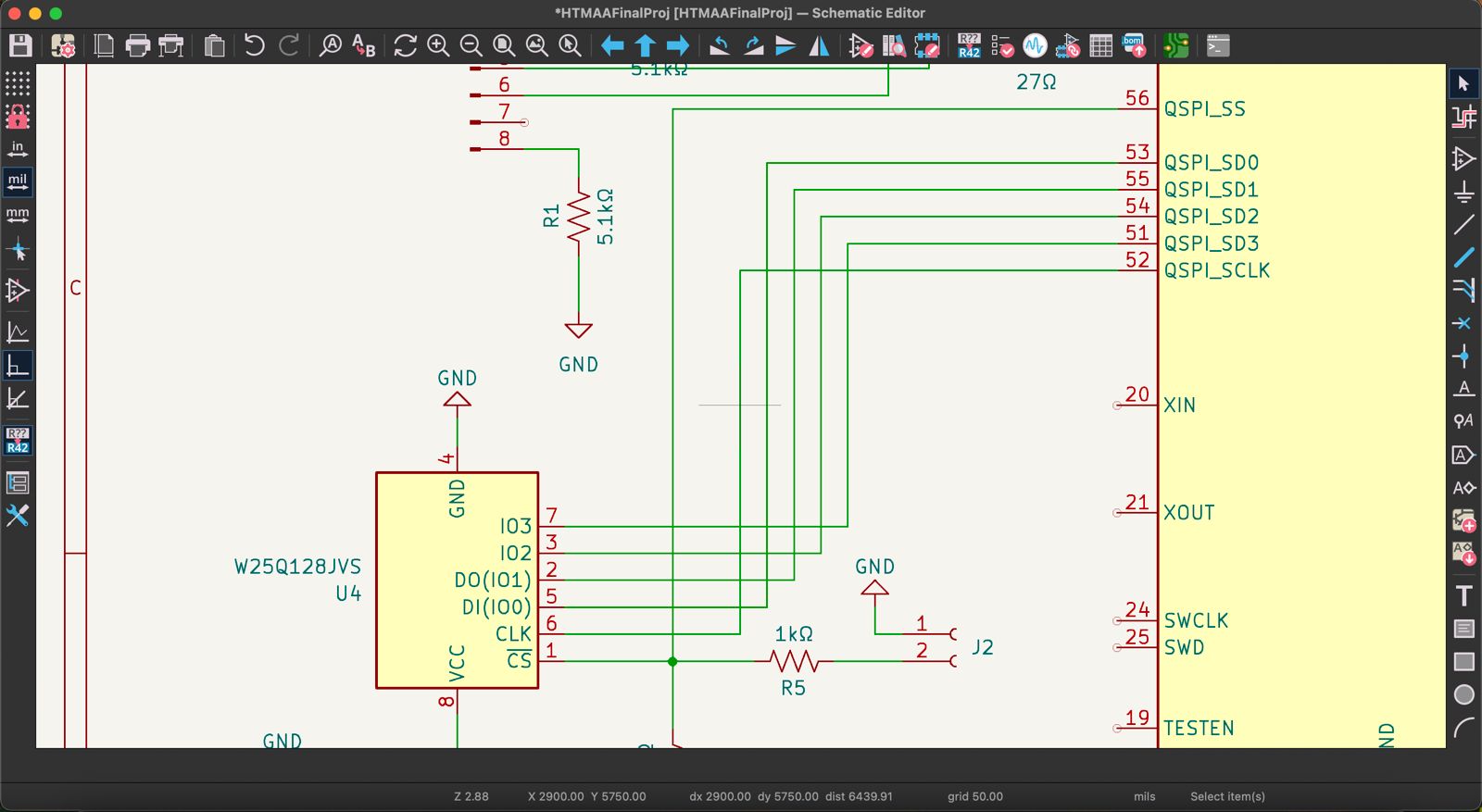
The next step is adding a flash memory system to allow the RP2040 to store program code, which it can boot and run from. The Winbond W25Q128JVS is a flash memory (quad SPI) integrated circuit recommended by the RP2040 datasheet which I added. Because this databus should frequently used, the pins should be connected directly via a short trace and also to minimize crosstalk with other circuitry. The QSPI_SS pin needs a pull-up resistor to the 3.3V supply and another to be used as the "bootstrap", for booting logic using a 2-pin socket header. The QSPI pins are then connected to corresponding pins on the RP2040.
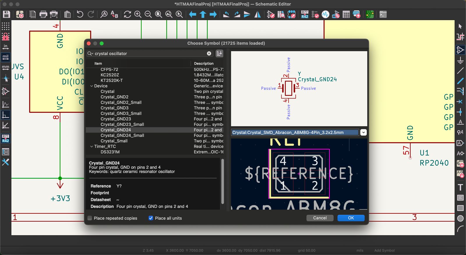
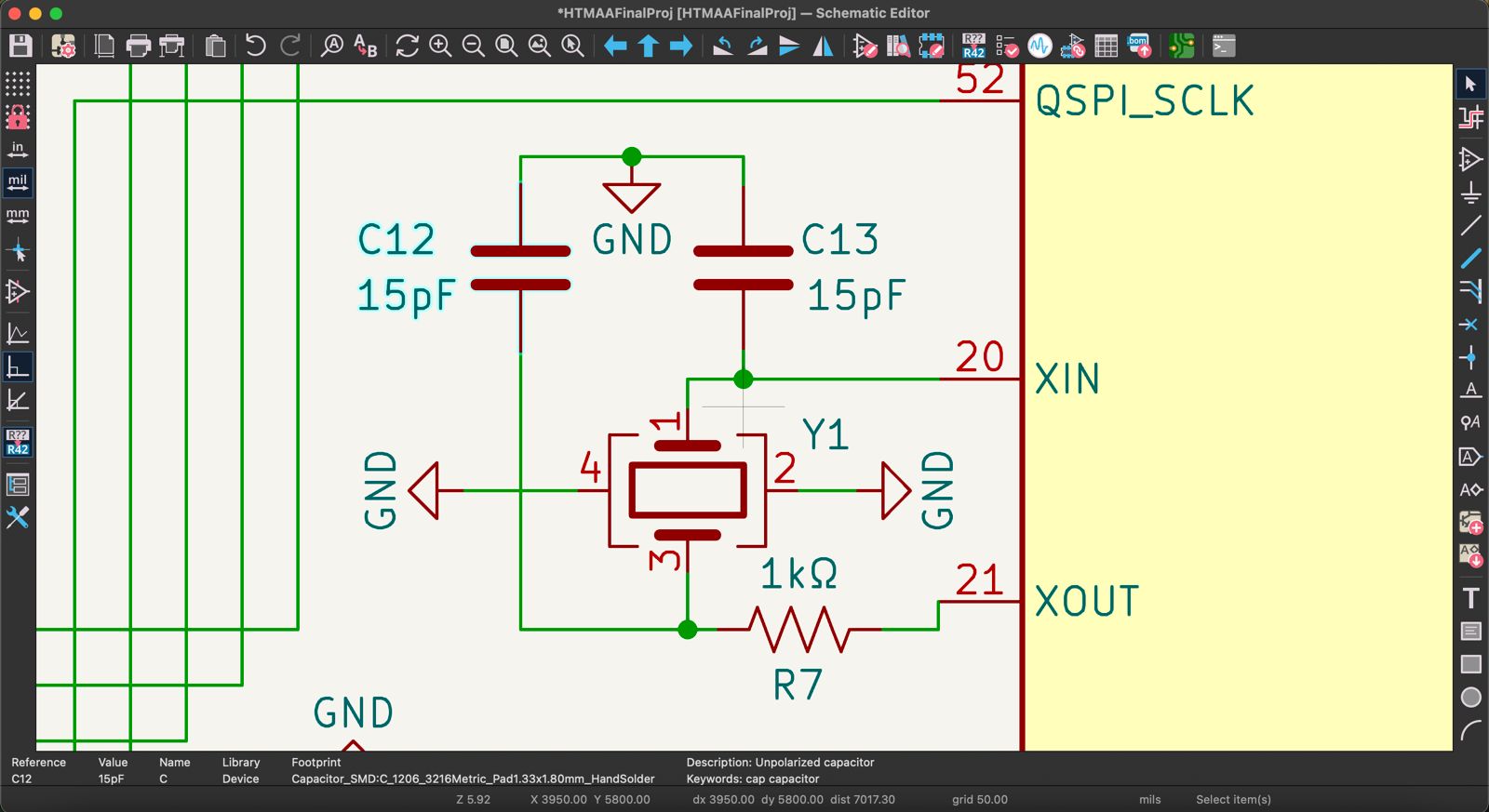
The final hardware addition we need for the RP2040 is a crystal oscillator as an external clock source. Although the MCU has an internal one, the datasheet recommends adding a frequency source for stability. The circuit connects a 12MHz cyrstal oscillator between the XIN and XOUT pins, with accompanying resistors and capacitors. Now we have assembled the RP2040 circuit with adequate power, memory, and clock source.
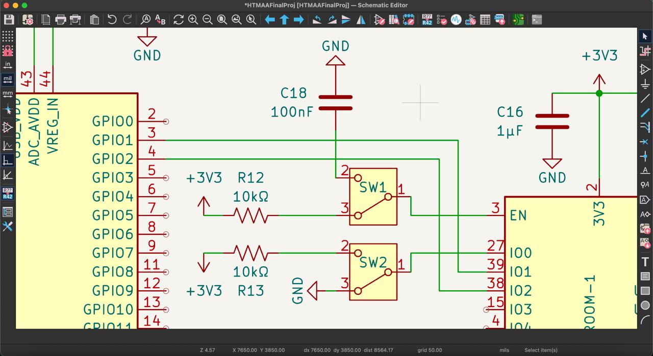
We have been ignoring the ESP32. Thankfully, the WROOM module already comes with the flash andn oscillator circuitry installed, so we will only need to add a power rail / databus (we can mimic the circuit used for the RP2040). This means we need to add a second USB-C connection, connect from a different COM port on my computer, and each MCU will have its own software program to run. However, the ESP32 only has a hardware boot trigger while the RP2040 can also be triggered via software (ex. the Upload button in the Arduino IDE). This means we need to add BOOT and EN buttons to the MCU to help with programming / debugging just in case, which is done with pull-up resistors. If the GPIO is HIGH (aka the button is not pressed), the ESP32 runs the main program. When the GPIO is LOW (aka the button has been pressed) the chip reboots and loads the new program. We will connect the BOOT / EN pins to the 3.3V power with a 10kΩ, with a 100nF capacitor for stability, each with an open push-button that closes the circuit to GND when pressed.
ESP32 PowerPush Button SwitchEN BOOT Circuit
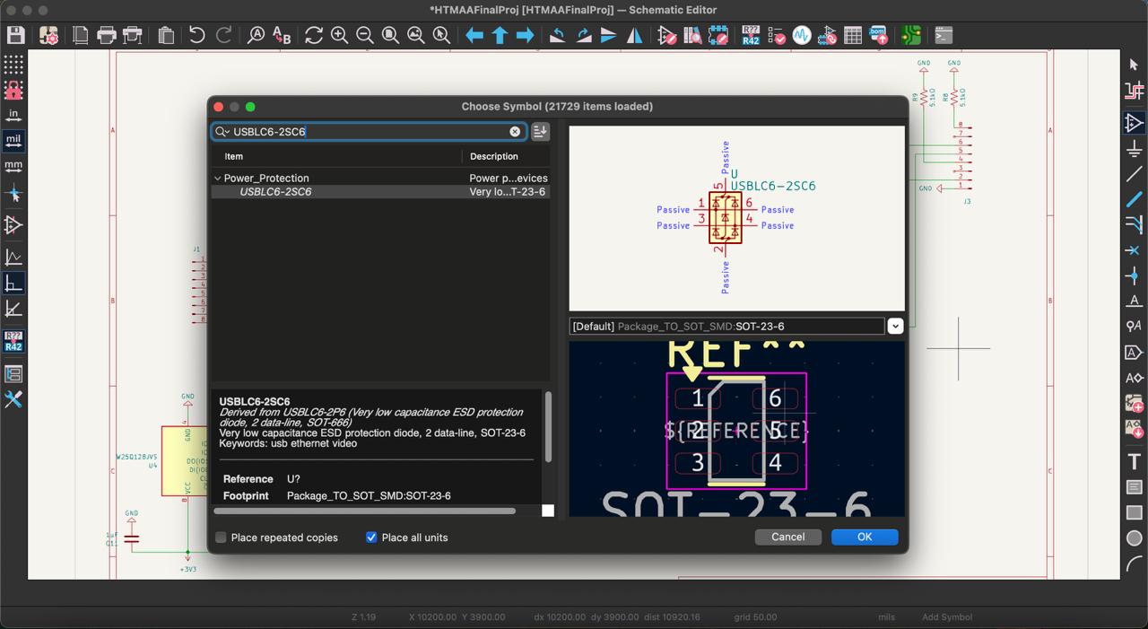
The last thing we need to add for stable, functioning MCUs is electrostatic discharge (ESD) protection. This shields the chips from damaging sudden voltage spikes, like when your fingers get shocked touching something. This is done by adding a TVS Diode array IC to the USB-C power connection that does not interfere with 3.3V range signals. I placed the USBLC6-2SC6 component between the USB-C data lines and to the 27Ω resistors, which is a very simple add. Now we have two functioning MCUs connected over UART protocol, and we can start building the rest of the system with LiDAR scanning and other sensors.
TVS DiodeESD Protection USB-CDual MCU Circuit
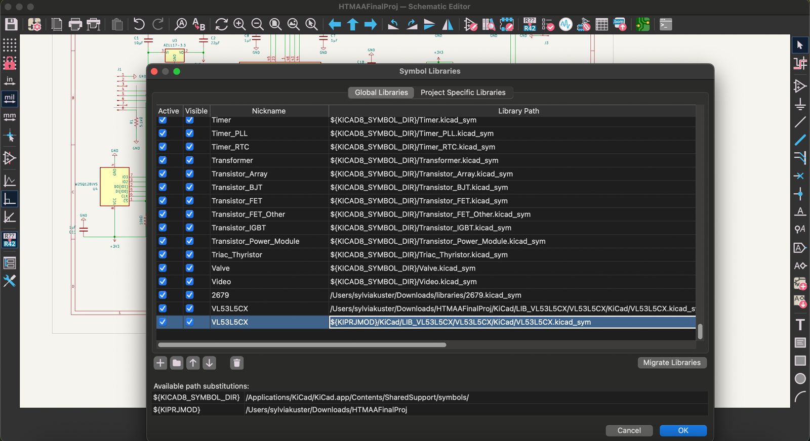
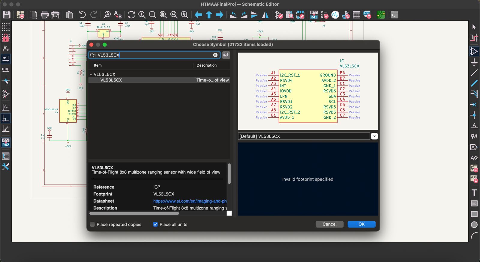
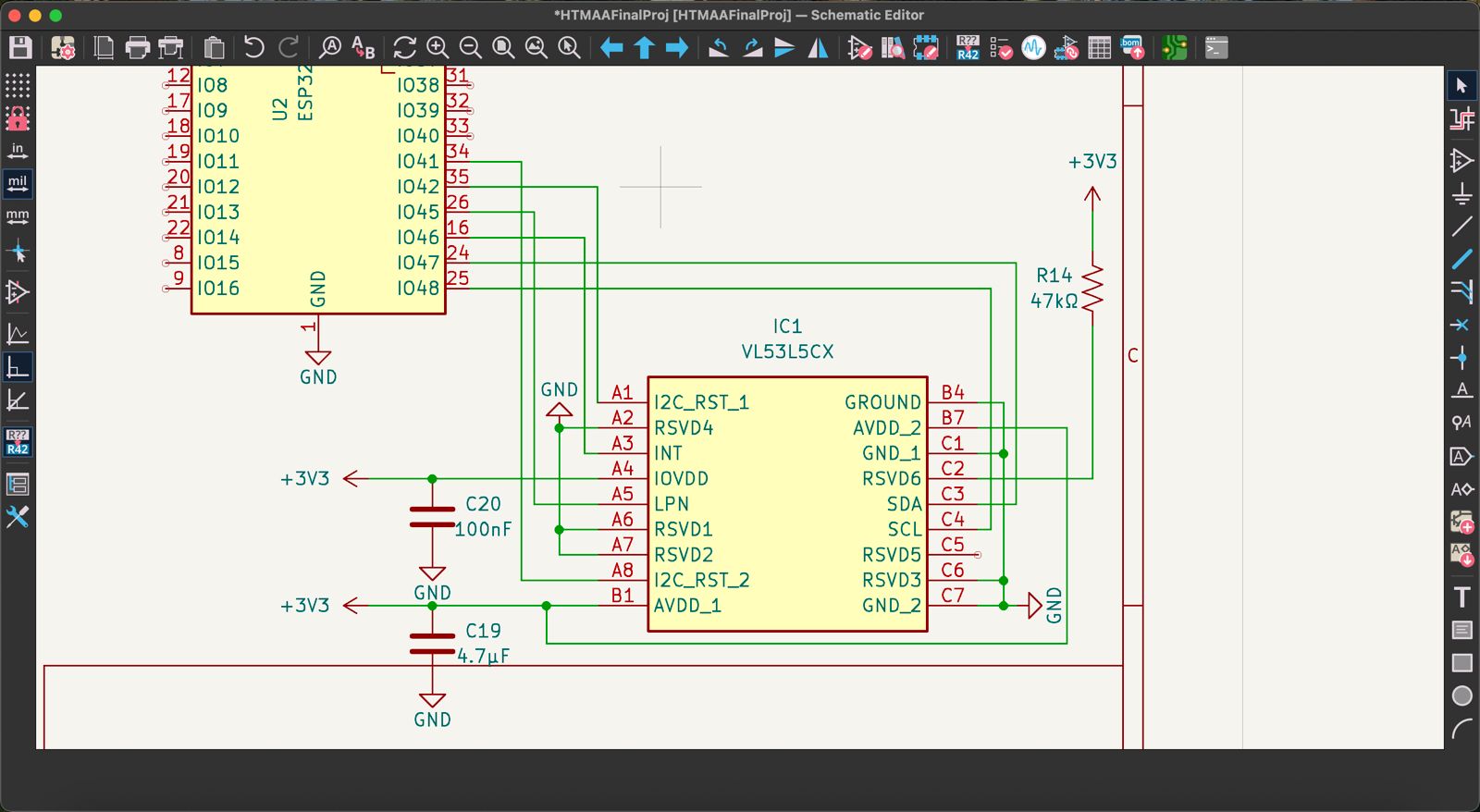
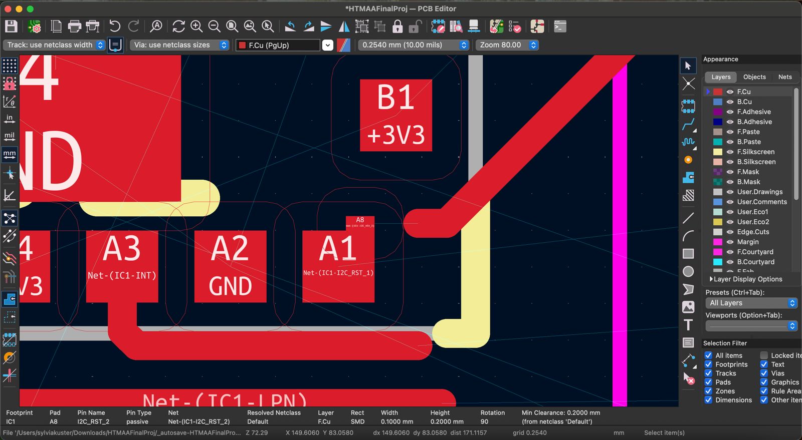
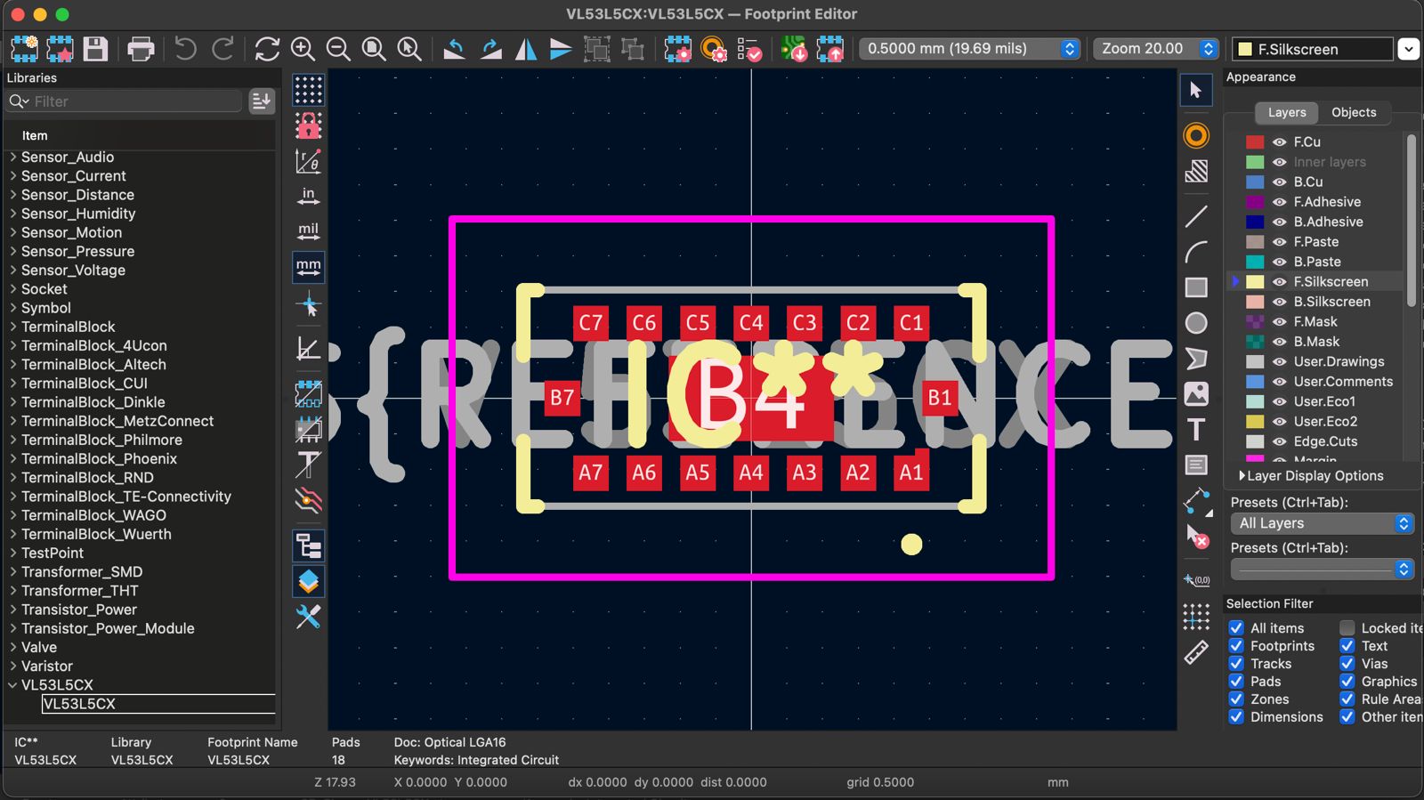
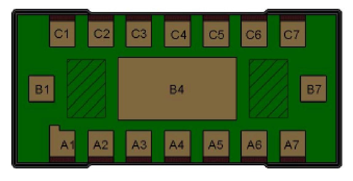
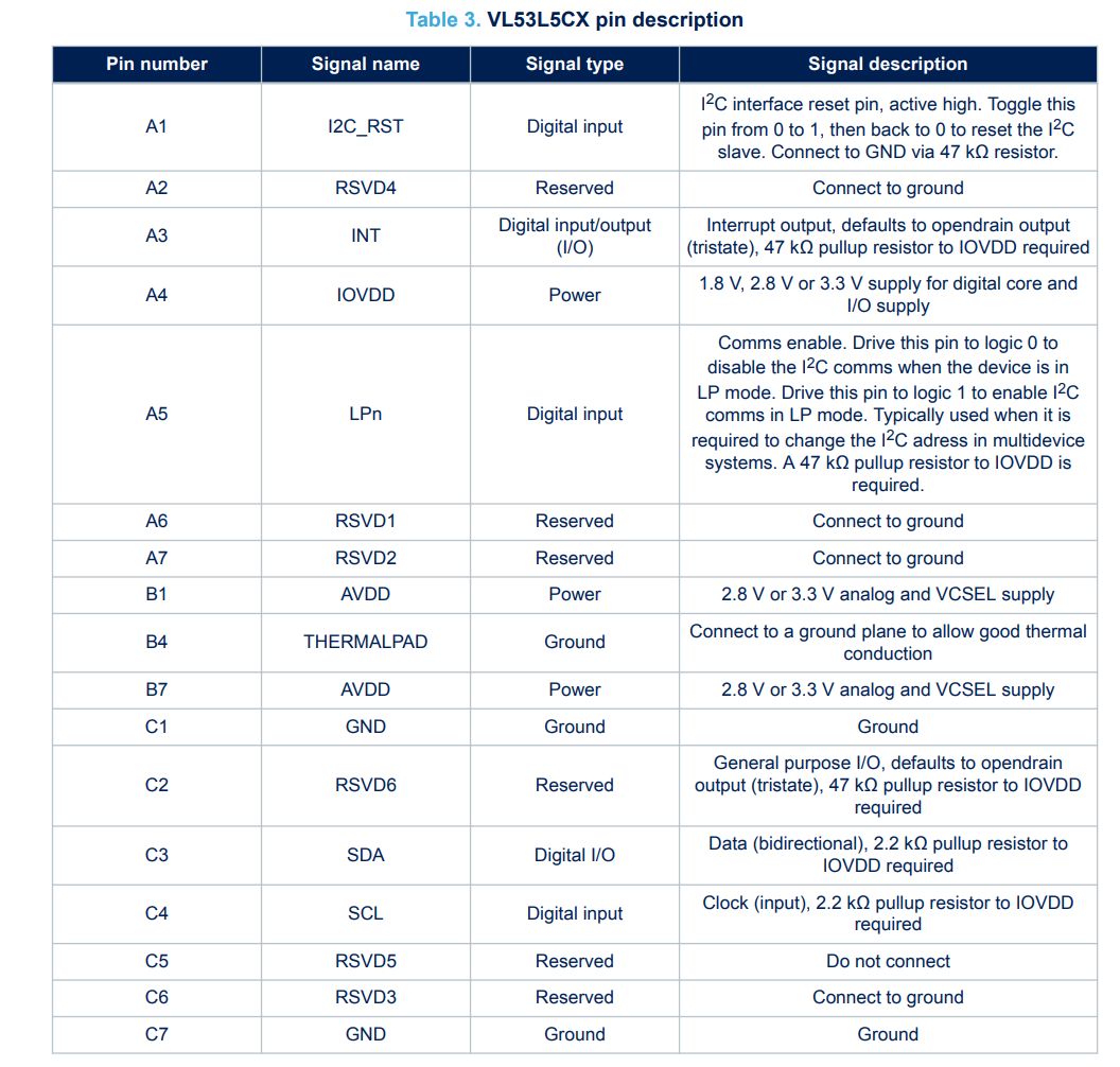
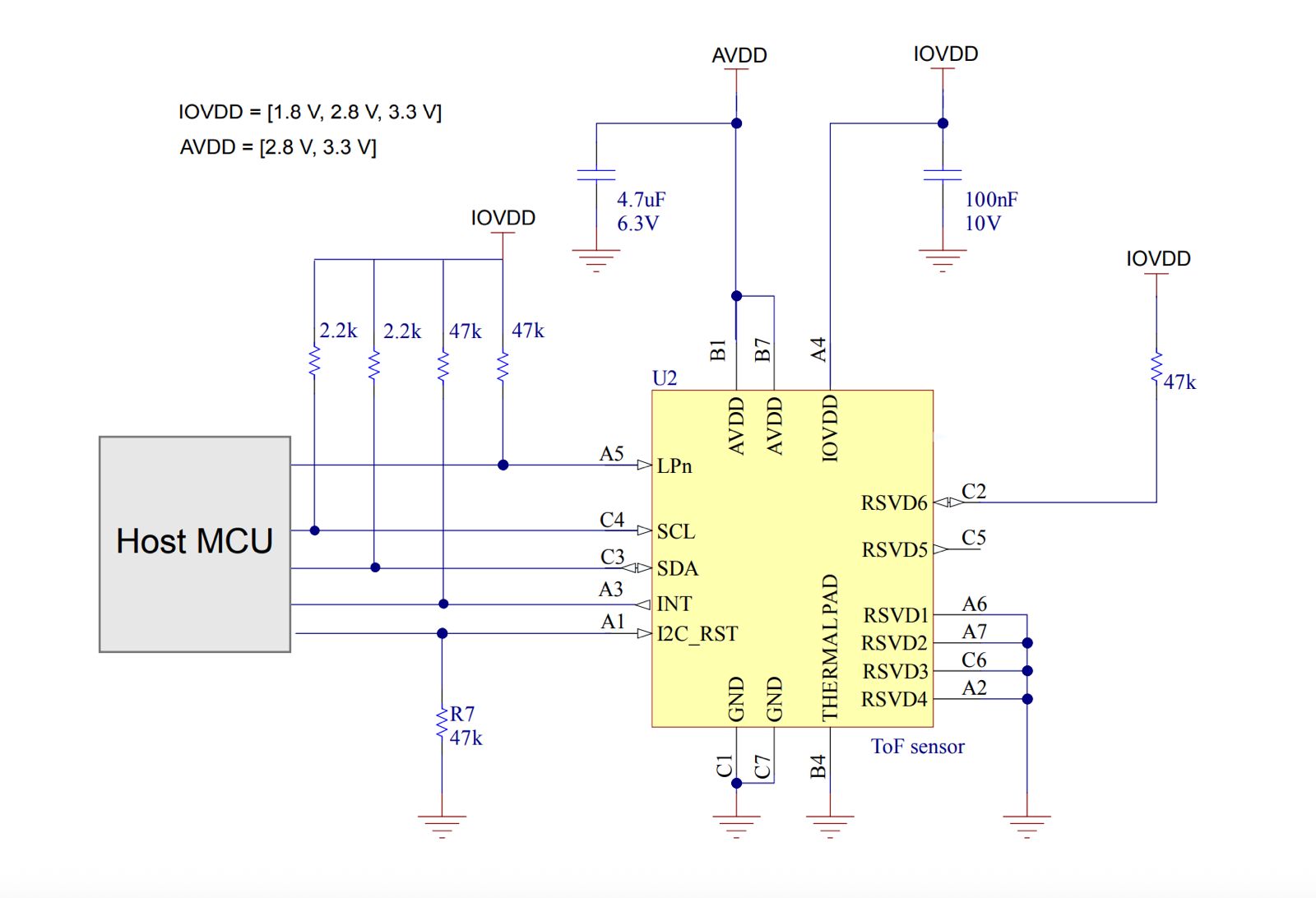
The first component needed for the laser device is a LiDAR scanner. The class inventory has the VL53L5CX module which provides a 3D depth map of the surroundings, with up to 1mm resolution and 4m range. However, the part symbol was not available on KiCad, so I downloaded a model on Component Search Engine and added it to the KiCad symbol library. I decided to use the ESP32 to handle the LiDAR tasks because of higher RAM and Wi-Fi capabilities, so I connected the VL53L5CX I2C pins to it that communicate the 8x8 (64-zone) depth map. The connections can be broken down into four main categories:
Power (A4, B1, B7): connect to 3.3V rail
Ground (C1, C7, B4): connect to common GND
Communication (C3, C4): I2C data and clock line are the SDA & SCL pins, connect to ESP32
Control (A3, A5, A1, A8): Interrupt, reset, and shutdown pins connected to power or ESP32
The remaining pins are left floating or grounded. I connected the comm pins to the MCU IO pins and followed the datasheet for accompanying circuitry (capacitors, resistors, etc). The ESP32 is flexible and can assign the I2C or Interrupt to any of the IO pins, and the pull-up resistor or decoupling capacitor principles hold here, too.
Adding Symbol LibraryVL53L5CX SymbolLiDAR Circuit
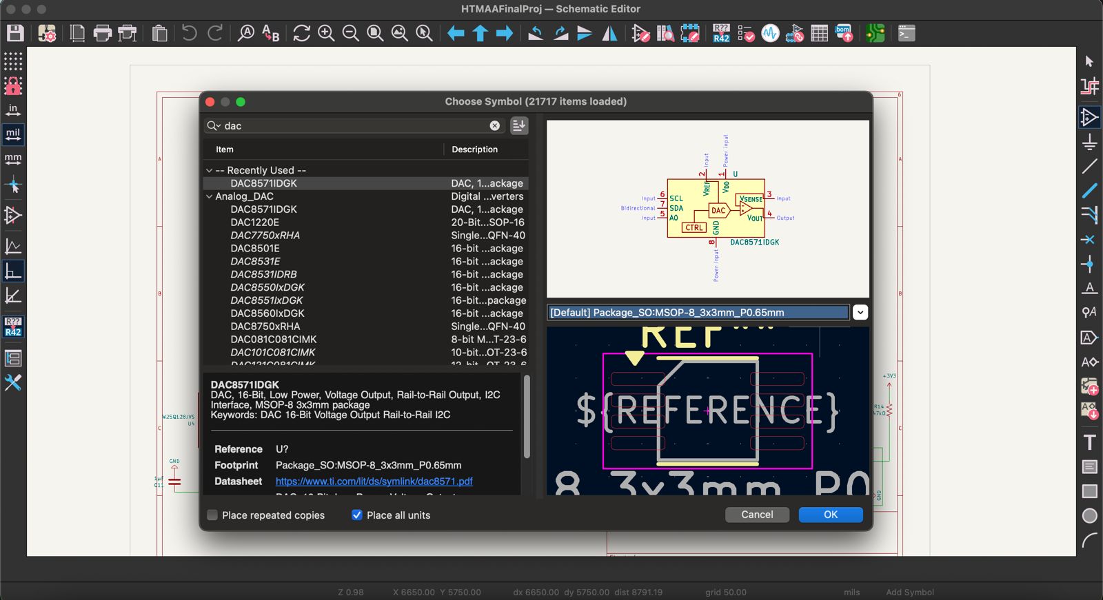
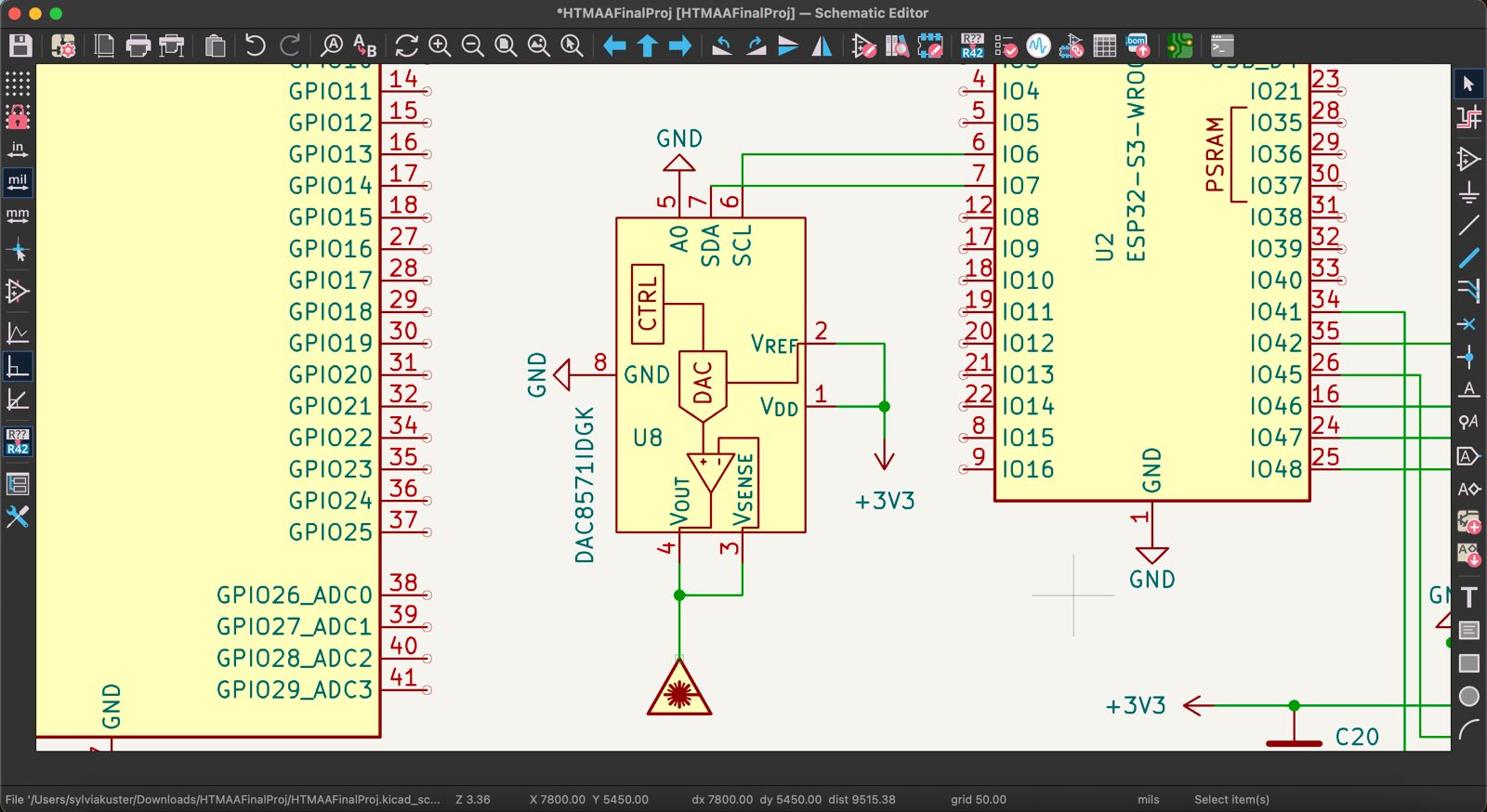
To iron out this final project, I did some more research on the types of LiDAR scanners and higher wattage lasers available. This project is the right candidate for a galvanometer laser, which uses mirrors to deflect the LiDAR beam along the XY axes. Once the LiDAR has detected a mosquito, the same galvanometer mirrors would instead direct the high power laser and hopefully hit the mosquito. The VL53L5CX component might no be the right fit, as it only provides 64-zone depth map which might not have enough resolution for this application. For now, I will include it in my sketch and pair it with a laser diagram to illustrate the concept. The galvanometer is an analog motor and the driver requires an analog signal from our ESP32 module, so we will also add a DAC component which will be attached to the galvo set. That will be my completed schematic circuit for now.
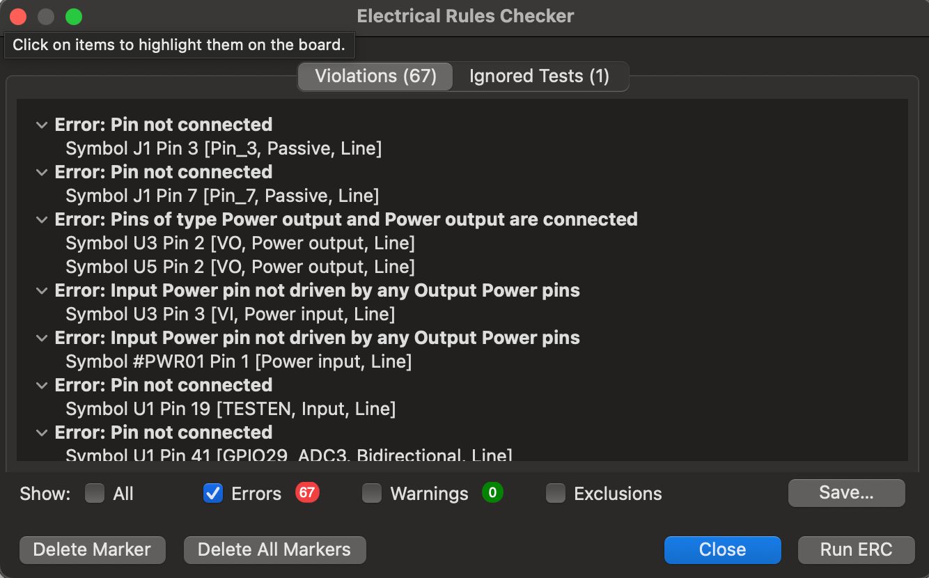
Once the schematic is assembled, it is important to use the Electrical Rules Checker and make sure that your design is not problematic. Go to Inspect -> Electrical Rules Checker -> Run ERC. My ERC resulted in errors related to many pins being left unconnected, which is not a major problem so I will intentionally leave it as is. If there is a clear short (ex. the outputs of two different regulators connected) then the design must be changed before moving on to the PCB Editor. The last thing is also to ensure that all footprints have been assigned for the components, which I confirmed mine were.
Run ERC ListERC Error Schematic
PCB Editor
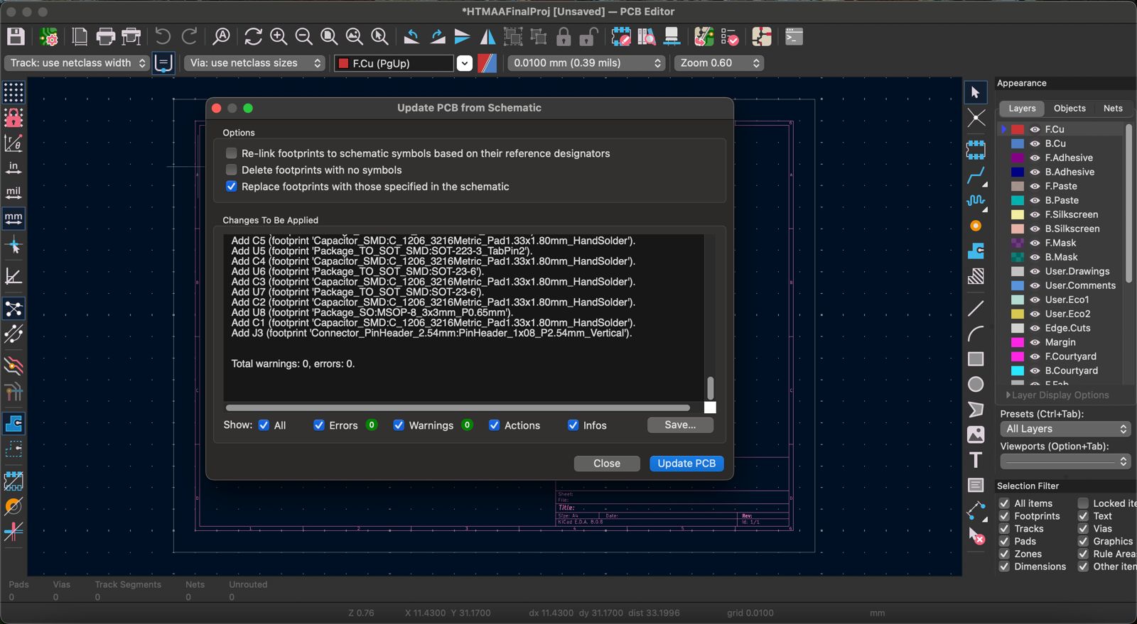
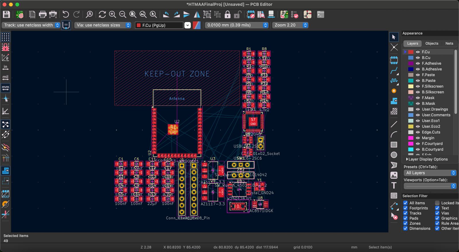
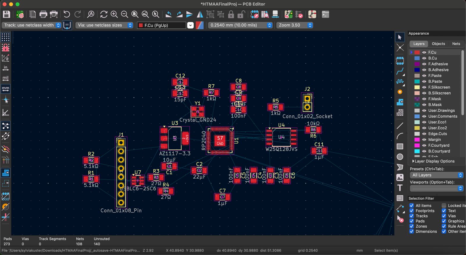
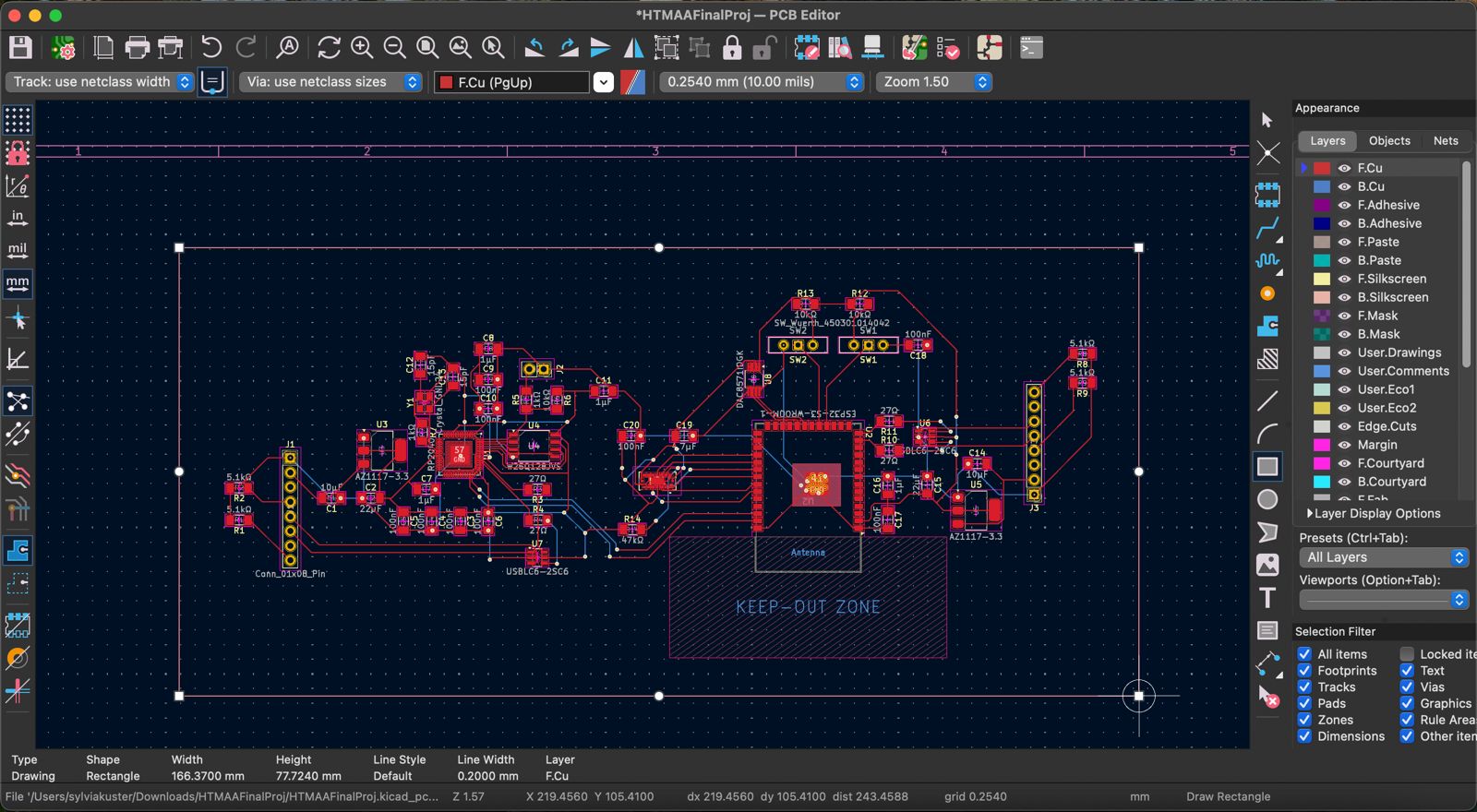
Once the schematic is done, the PCB Editor is used to physically design the placement of components on the board. I updated the PCB from the Schematic and verified that there were no errors. The "rat's nest" loaded in with all the logical connections (light blue lines shown) between pins and components which I had to untangle and properly place.
Update PCBRat's NestLogical Connections
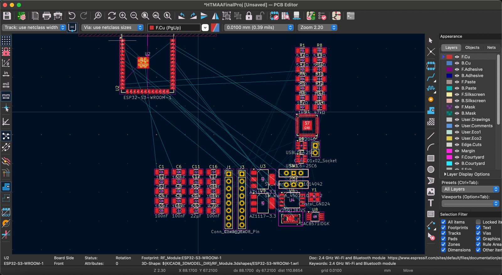
This is where the real game begins, as I tried to optimally place components to minimize crossovers. I started to work on the RP2040 module because of its standalone flash memory, crystal oscillator, and USB-C connections. Whenever there was an inconvenient connection between two pins, I sometimes was able to go back to the schematic and logically connect it through another route and then updating the PCB. This helped reduce the lines crossing over and make the routing simpler.
RP2040 LayoutESP32 LayoutSchematic Redraw
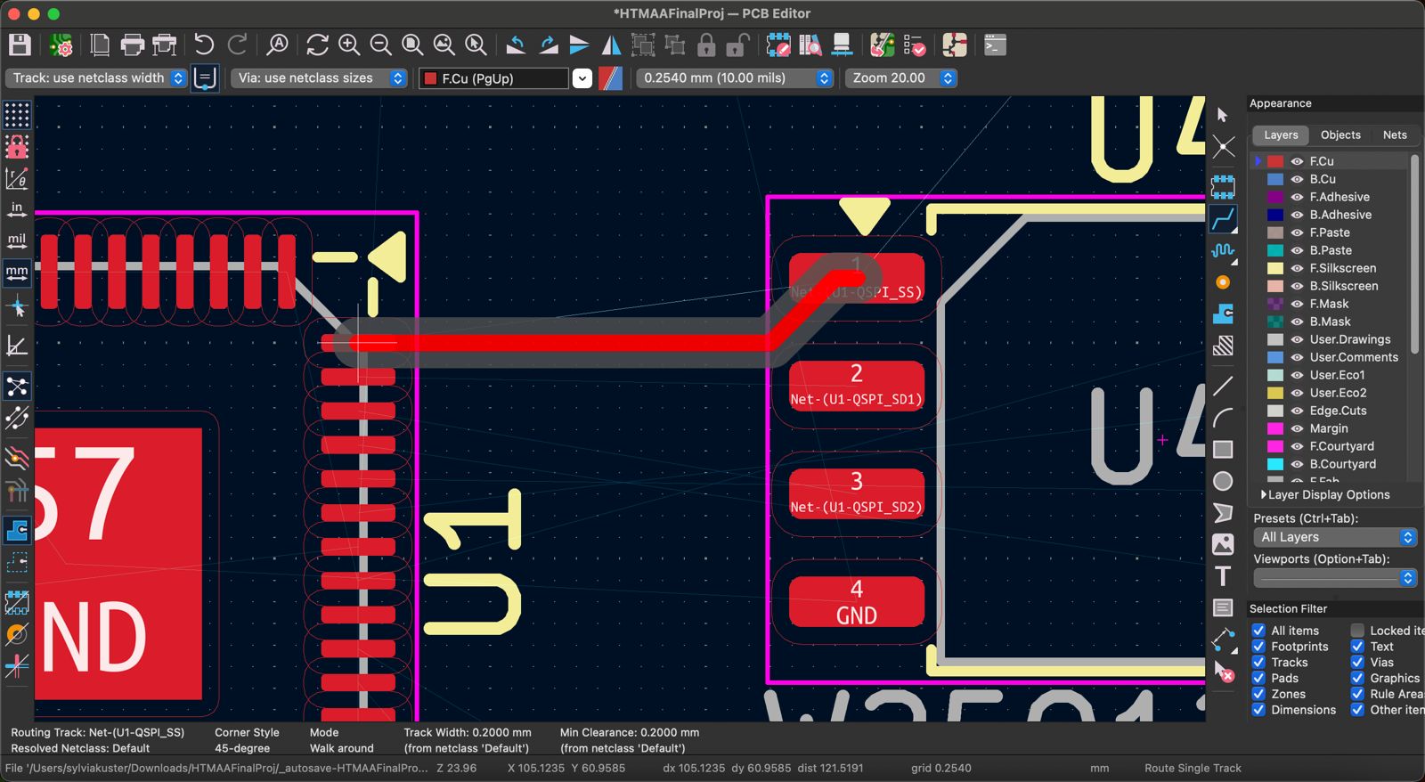
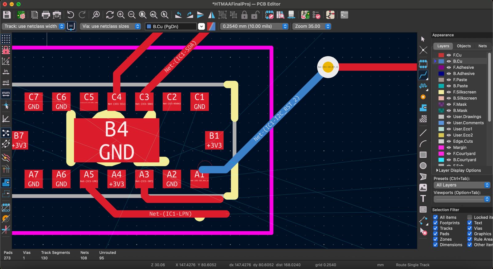
After I assembled everything in a general layout, I had to start laying down copper traces to connect pins. Vias, which are tiny holes connecting the bottom and top PCB layers, were also used to help overcome the crossovers sometimes. I started with connecting the Winbond flash memory and the RP2040 processors, making sure to keep the copper traces as short as possible to reduce latency. Selecting the wire symbol in the right menu and the red F.Cu tool, I started laying down the traces. As a via example, the VL53L5CX has a pin (A8) that is on the bottom of the pad so I connected the trace to a via that routed it on the bottom layer (B.Cu).
PCB Editor TraceA8 Trace FailA8 Via Solution
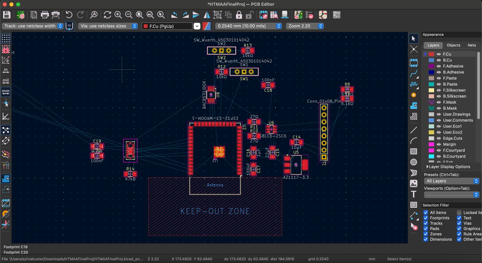
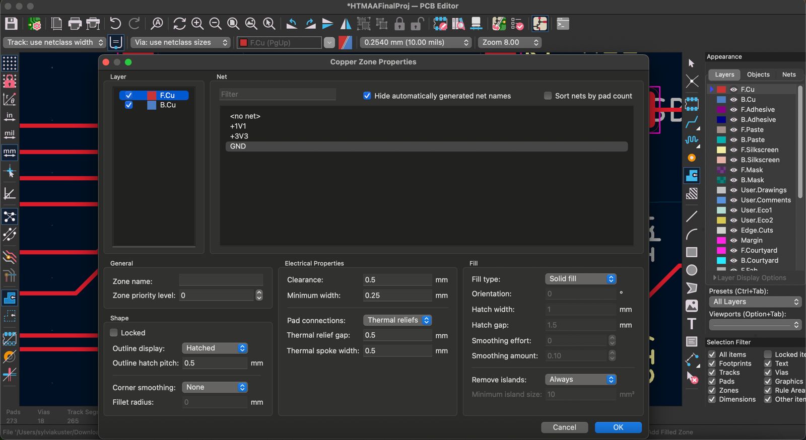
Once all pins were connected, the last thing I had to do was make sure there was a common ground between the two MCUs. I created ground pours beneath each MCU by using the Filled Zone function, selecting the area, and pressing the B key. Additional ground connections were made through copper traces and vias to this ground pour. Finally, I created a rectangle using Edge.Cuts around the PCB to delineate the boundaries for manufacturing.
Filled Zone ToolGround PourPCB Layout
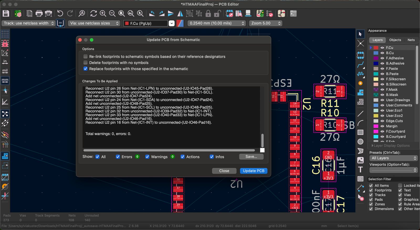
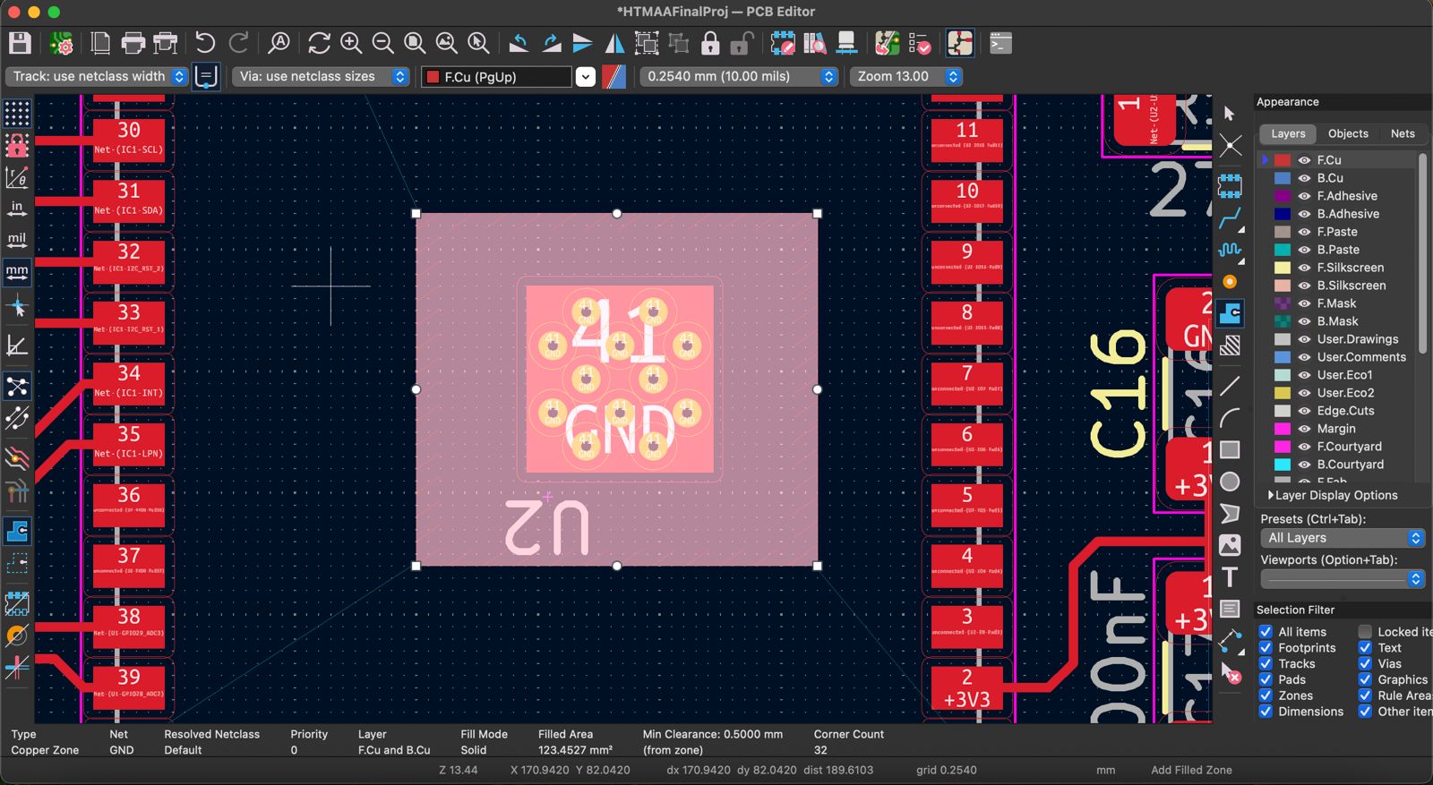
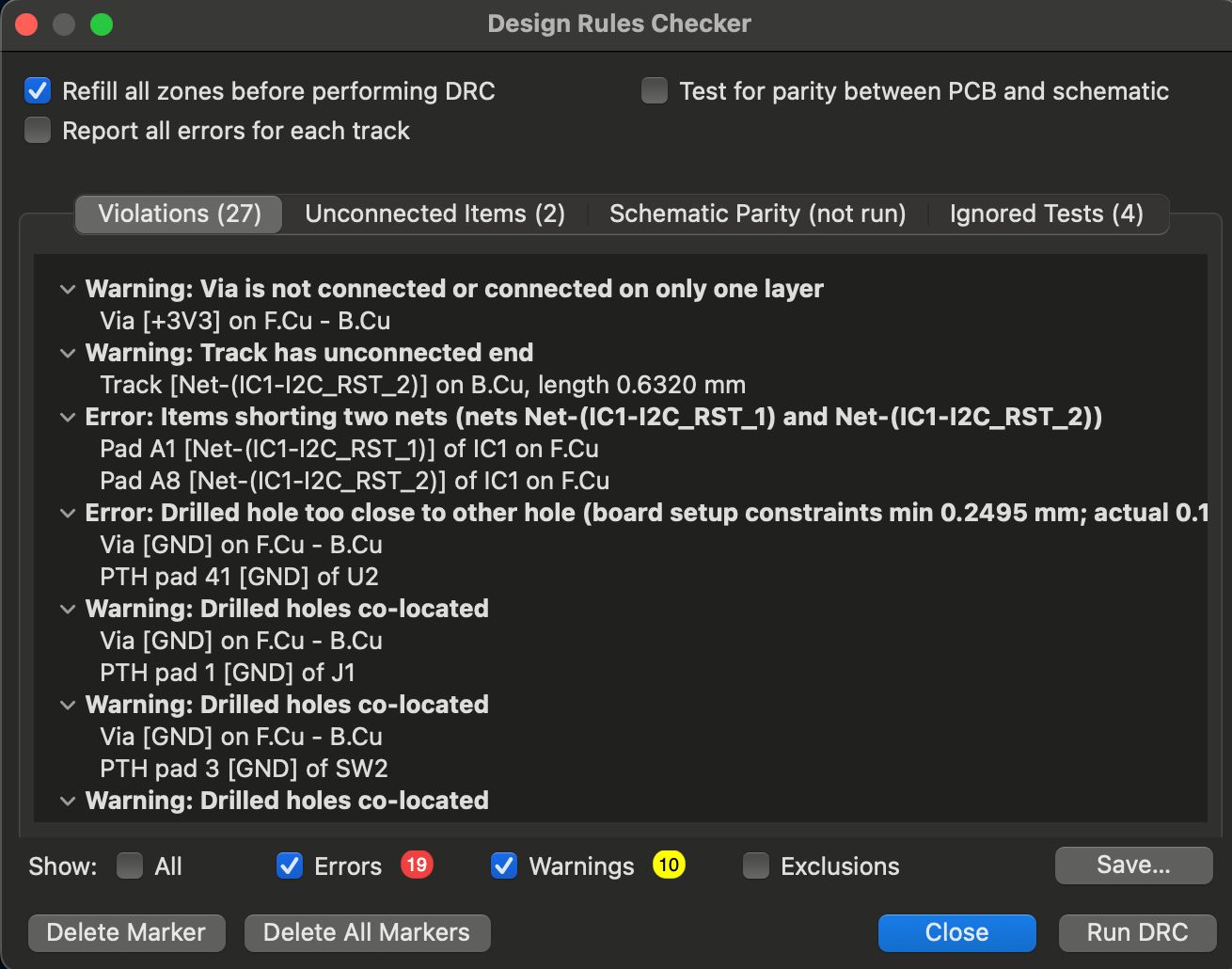
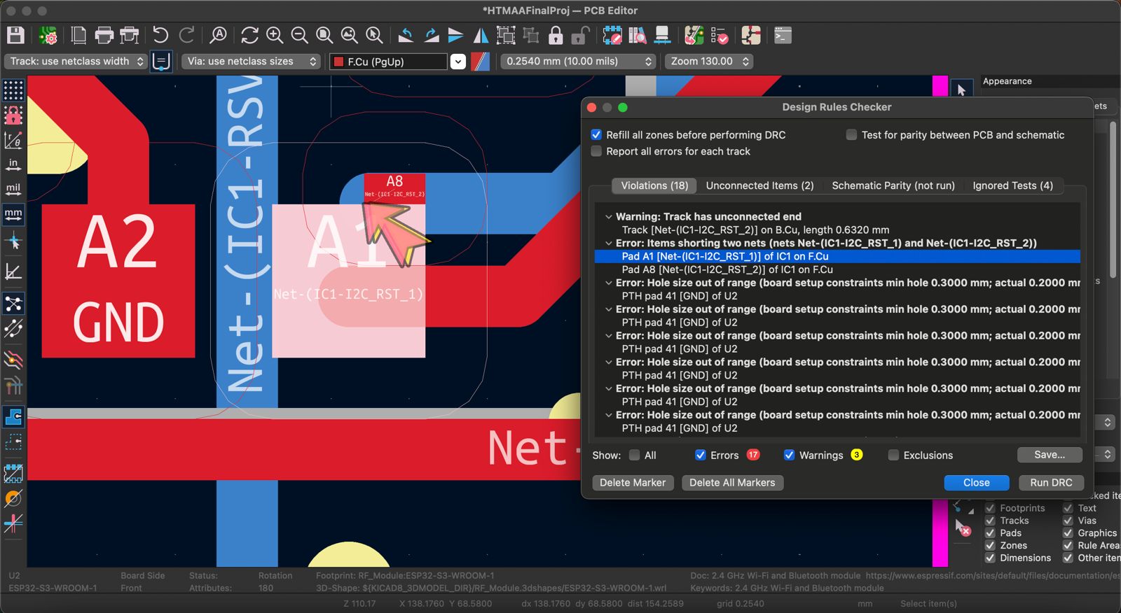
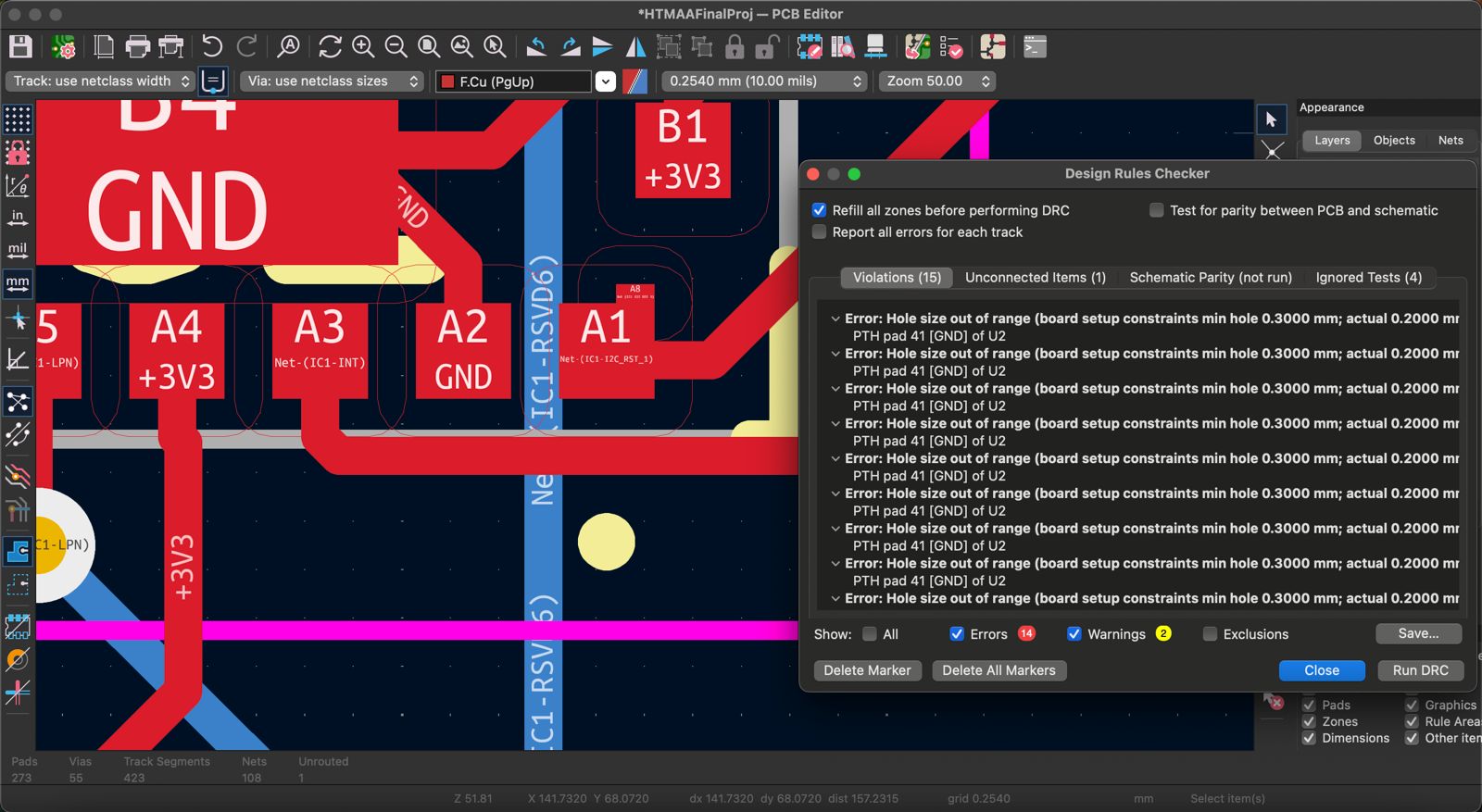
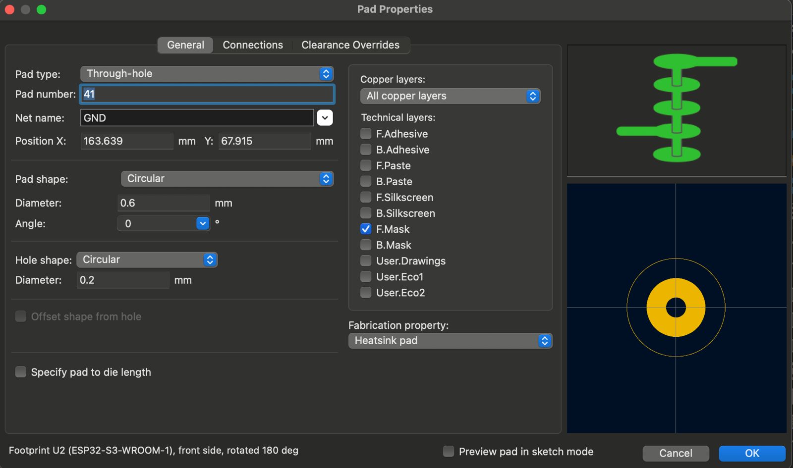
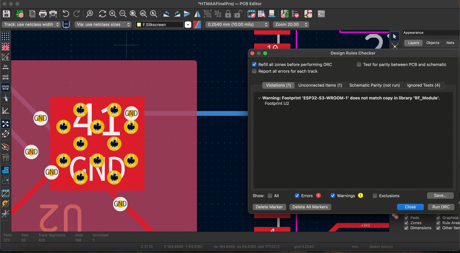
I ran the Design Rules Checker (DRC) to determine any board setup errors. The first one I noticed was about the A8 pin on the VL53L5CX module overlapped / shorted with A1. I decided to check the Footprint Editor and realized by referencing the datasheet that there should not even be an A8 pin with independent connection with the ESP32. I went back to the schematic and integrated it with A1 (the real I2C_RST channel). The second error was that the GND vias pre-loaded under the ESP32 board used for thermal diffusion had small hole diameters (0.2mm vs 0.3mm min required). I went through and edited the Properties by selecting the E key and altering the hole diameter to 0.3mm. Once this was finished, I had no errors left and could get started on simulating operation through Wokwi!
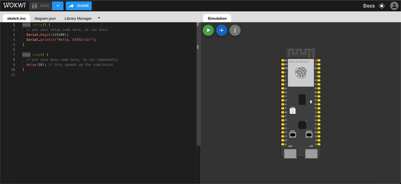
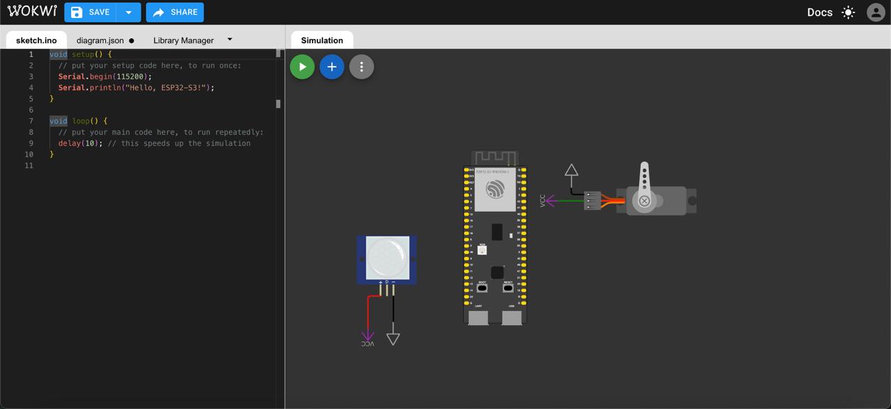
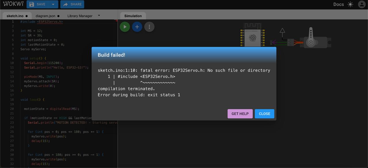
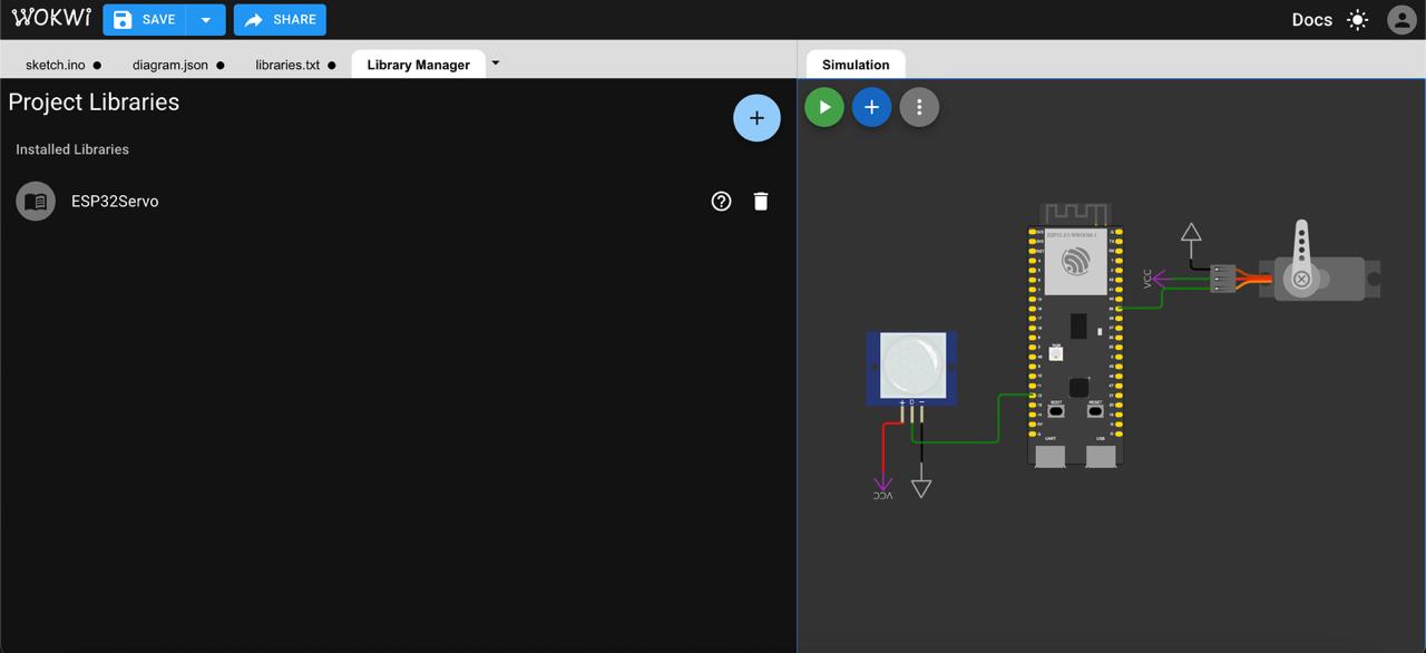
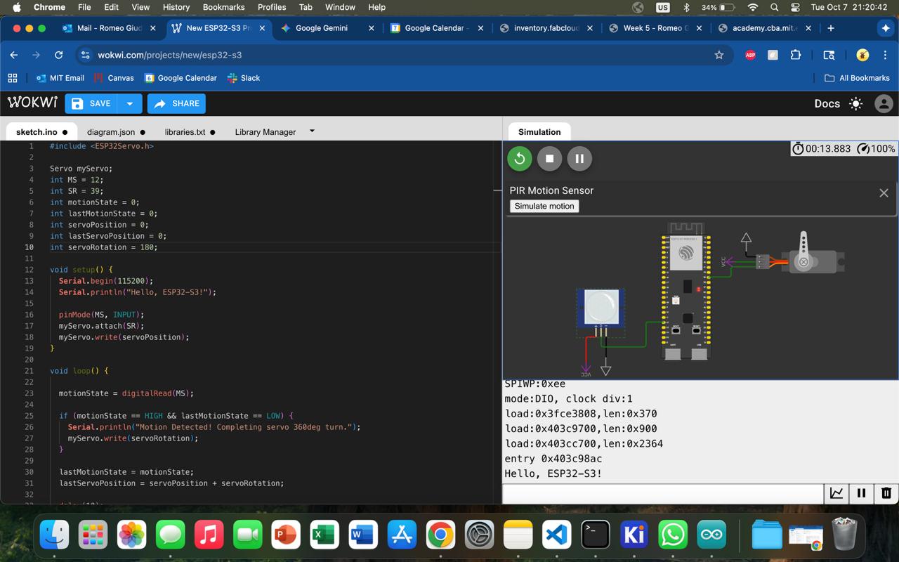
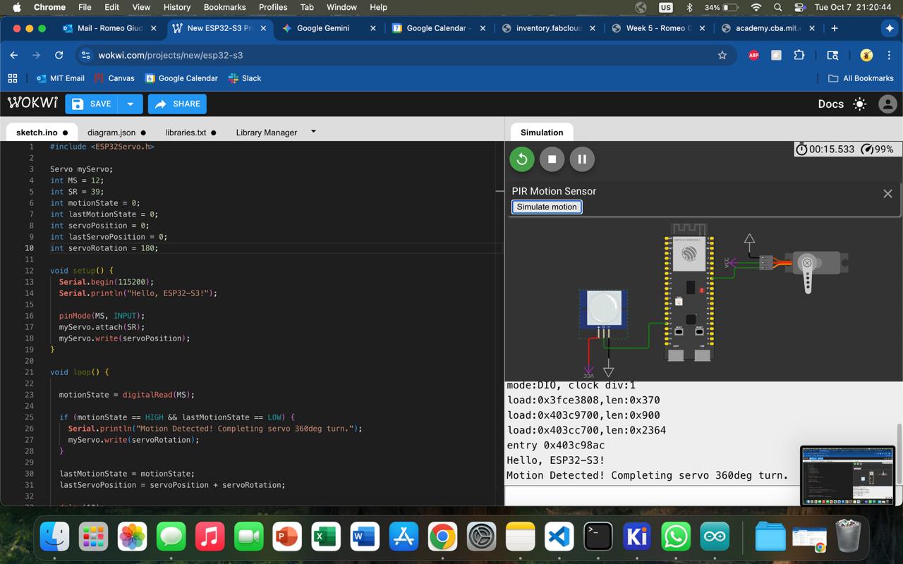
To simulate operation of a PCB design, I created an account on Wokwi and created a new ESP32 Arduino project. The software allows you to design a circuit visually on the right half, and program the MCU on the left. I decided to return to the garden project idea and create a representation of the electronics of my bird feeder idea. This would include a motion sensor that can detect when birds come to the feeder, and spins a servo to give out food like a cereal dispenser. Once I connected the circuit, I began to write the C++ on the Arduino style interface. I defined the initial variables and values, along with the Serial Monitor. Then I programmed the logic that spins the servo when the motion sensor outputs a HIGH signal, indicating motion has been detected. This dispenses food to the birds and then returns to initial position after. The first run of code flashed the error sign: "sketch.ino:1:10: fatal error: ESP32Servo.h: No such file or directory". I then went to the Library Manager and added the ESP32 Servo library formally, which fixed the error.
During office hours on Thursday, our class TA Gert kindly showed a big group of us how to use the oscilloscope, multimeter, and regulated power supply for electronics. They are great tools for debugging potential problems with boards and isolating what to fix.
Oscilloscope: voltage signal changes over time, displayed as a waveform on a graph.
Multimeter: measures electrical properties (voltage, current, resistance) through metal prongs.
Regulated Power Supply: provides stable DC voltage to test electronics on the workbench.
Link to the Architecture shop site group assignment.