Week 5: Electronics Production
Project Plan
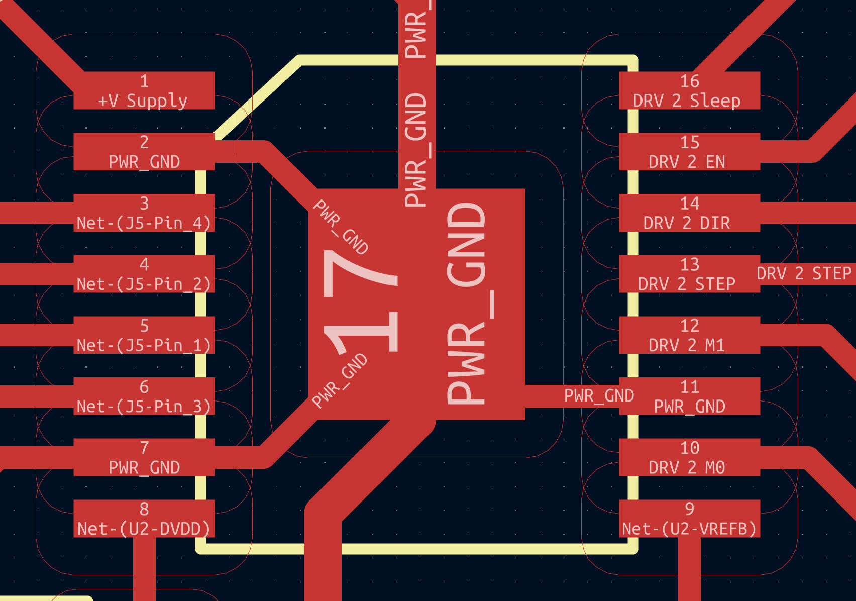
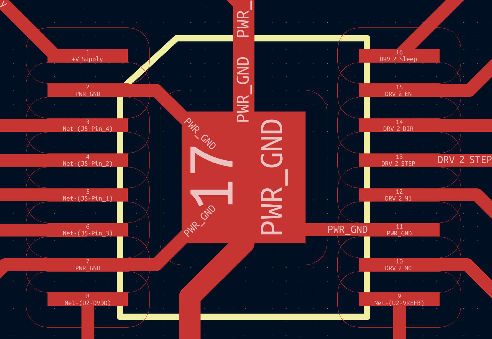
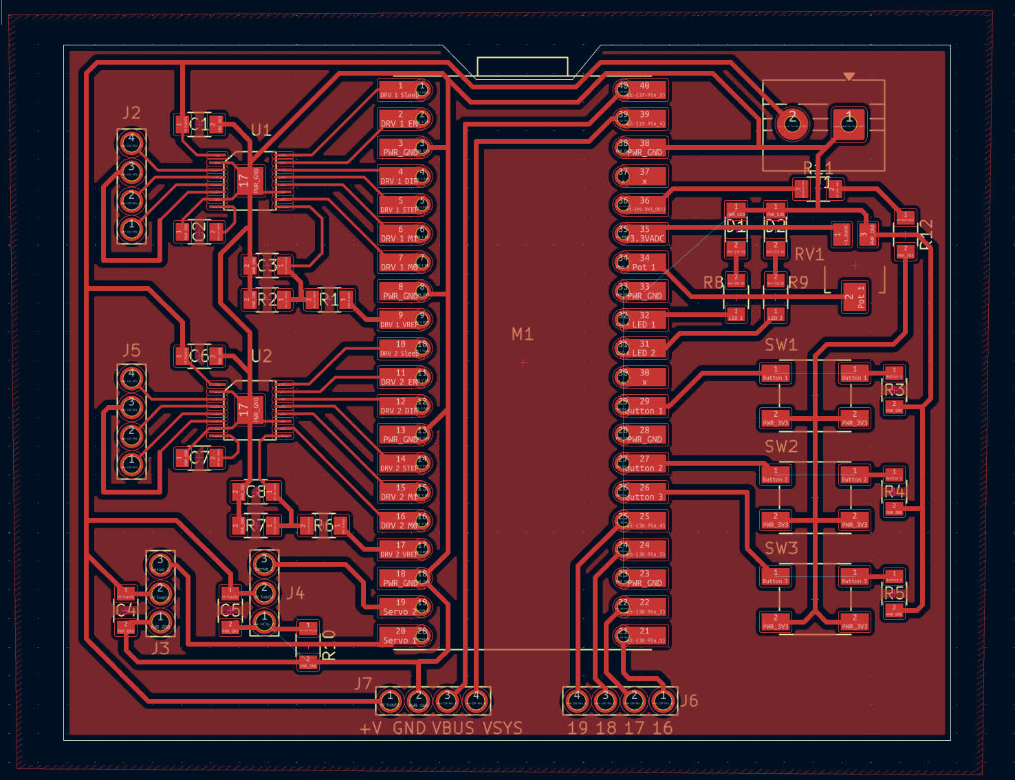
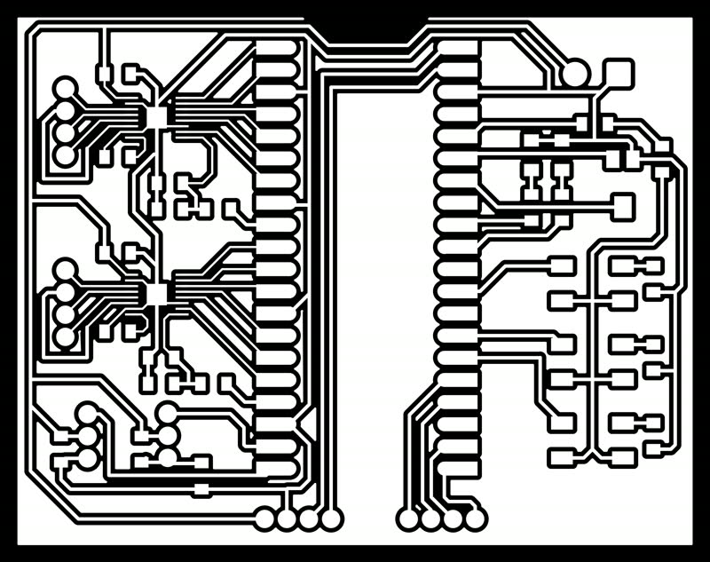
The general plan for this week is to manufacture the design from last week: the development board focused on stepper and servo motors. Before I go ahead and mill the PCB, I plan on going through the data sheet one more time to make sure that everything is connected as it should be. I also need to deal with the problem that I ignored last week, the pads on the original footprint of the DRV8428 are too small to be milled on our machine. I'll also need to go through and determine exactly what size resistors and capacitors I will need to include in my board.
The Training
I went to Jen's training on Friday to learn how to use the PCB mill in the Architecture Shop. We learned to use the Roland SRM-20. To use
this machine, we used the Mods which already has a program designed for the machine. To use Mods, we had to open it up through terminal
and then go through the website. Once on the website, we selected server programs and then found PCB mill under Roland SRM-20. With Mods open
all we had to do was open the desired PNG, and then select whether we were milling traces or cutting, calculate, and then send to the machine.
Regarding the endmills, we used the 1/64" endmill to cut the traces and then a 1/32" endmill to cut the holes as well as to free the board from
the PCB stock.
Group Assignment
To be added shortly...
Execution
I started my week by meeting with Anthony to figure out how to solve the fact that the DRV8428 pads were too small. He suggested simply going into the footprint editor in Kicad and modifying the size of the pads. If that didn't work, I could try using the engraving bit and tuning that in.
It turns out that modifying footprints is actually pretty easy! All you have to do is right click the component in the PCB editor and select
open footprint editor. Once in footprint editor, I was able to select one pad and reduce the thickness by 6.2 mil, just enough to make it so that
the endmill would fit between the pads. I found the 6.2 measurement by using the built in measuring tool and knew that I needed the gap to be 16 mil.


Milling the PCB
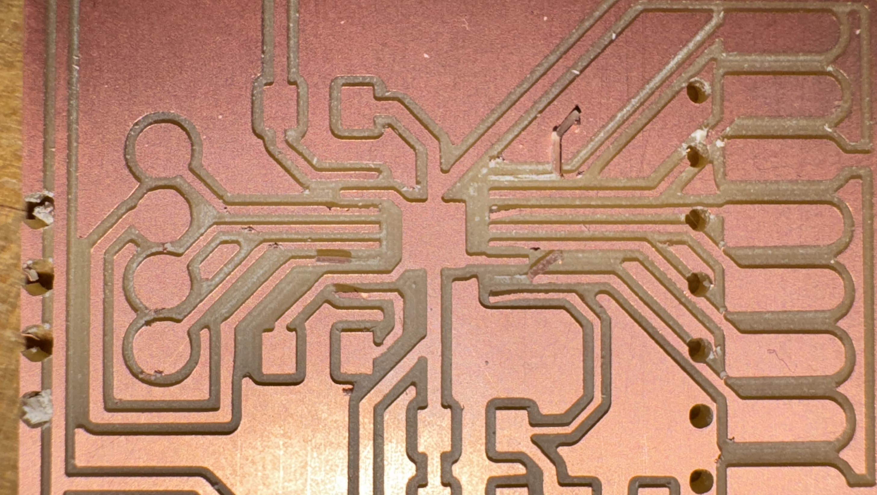
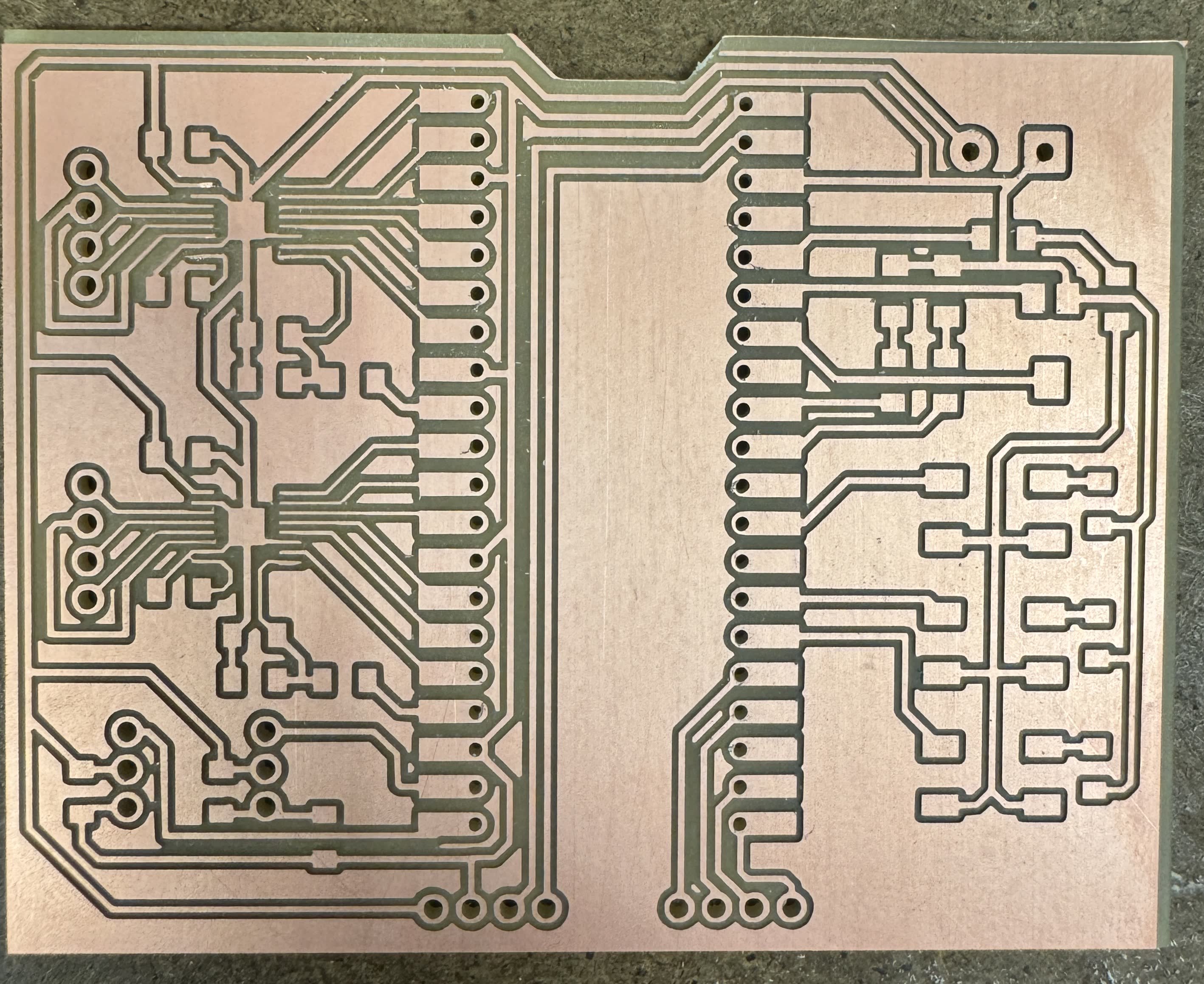
Alright, to cut to the chase, I tried milling my PCB three seperate times. None of which I can say turned out perfectly. Due to the complexity of the board,
milling the traces alone took about 25 mins and the edges and holes took another 10 mins. The first attempt failed for multiple
reasons. The most noteable was that the files did not line up with one another when they were run, hence, holes were drilled in the wrong spot and the edges
were milled in the wrong location. I didn't realize that when adding the images into Quentin's converter, I should have started with my largest image and
locked it and then added the trace PNGs after. I learned this in my second conversation with Anthony this week, more on that later though. I also learned
that you could add in multiple PNGs into one so you could for example cut the holes and edges in one run as opposed to having to run two seperate operations.
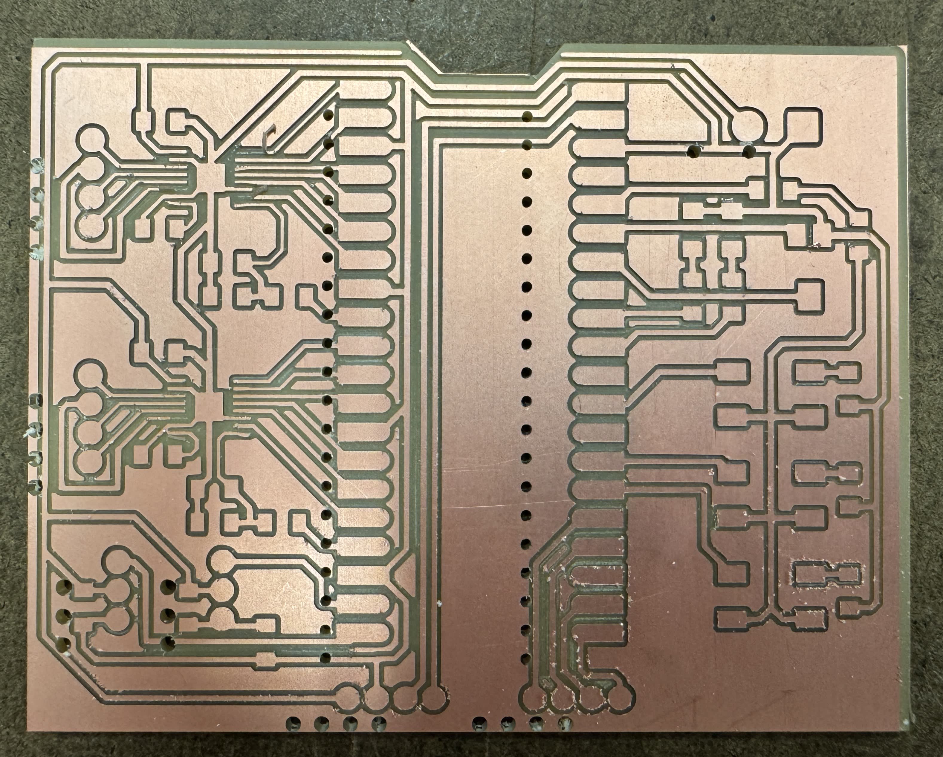
After talking with Gert, we decided that it would be worth trying again with a sharper endmill to see what would happen. I of course also reformatted my
PNGs with Quentin's converter to make sure that everyting would line up. While better, it also had some of the traces tear up during the milling process.
This sounds stupid but I have noticed over the past few weeks in my meetings with Anthony as well as other TA's, that they are far more productive, beneficial
and efficient if you come to them with a plan of exactly what you want to discuss. It wastes less of their time as well as your own.
Last week, I went to Anthony and sat there for about three hours asking questions periodically as I was doing work that I likely could have done in advance with
a little more research on my behalf. This week, however, I knew that I wanted to discuss how to solder the DRV8428s, make sure my Pico W was functioning, how to
approach the trace problem, grab a new screw terminal as the Arch Shop didn't have it in inventory, as well as a few more soldering questions. With that list in
mind, we were able to meet and answer all of those questions in less than 30 mins. Prior Proper Preperation Prevents Piss Poor Performance!
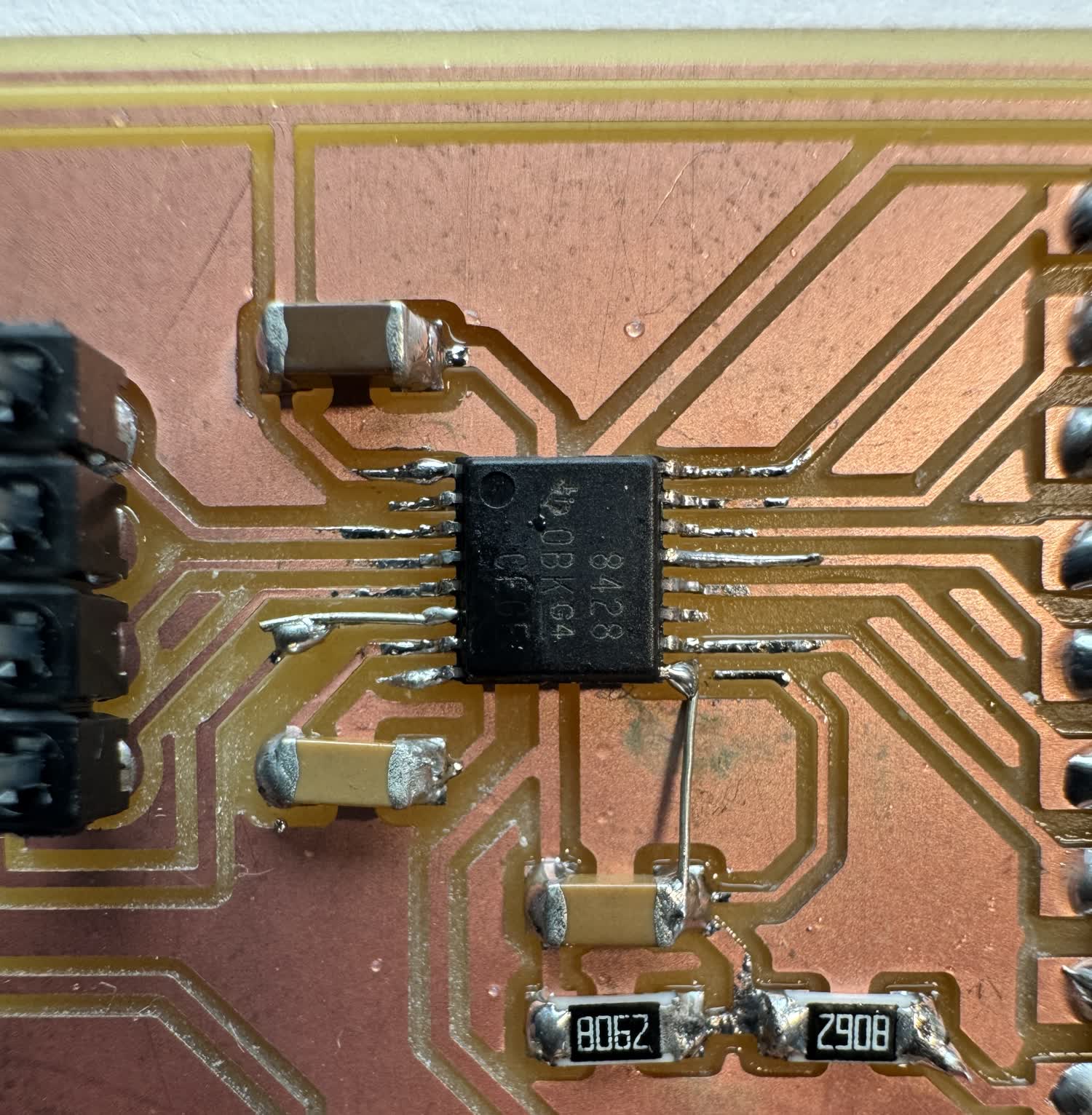
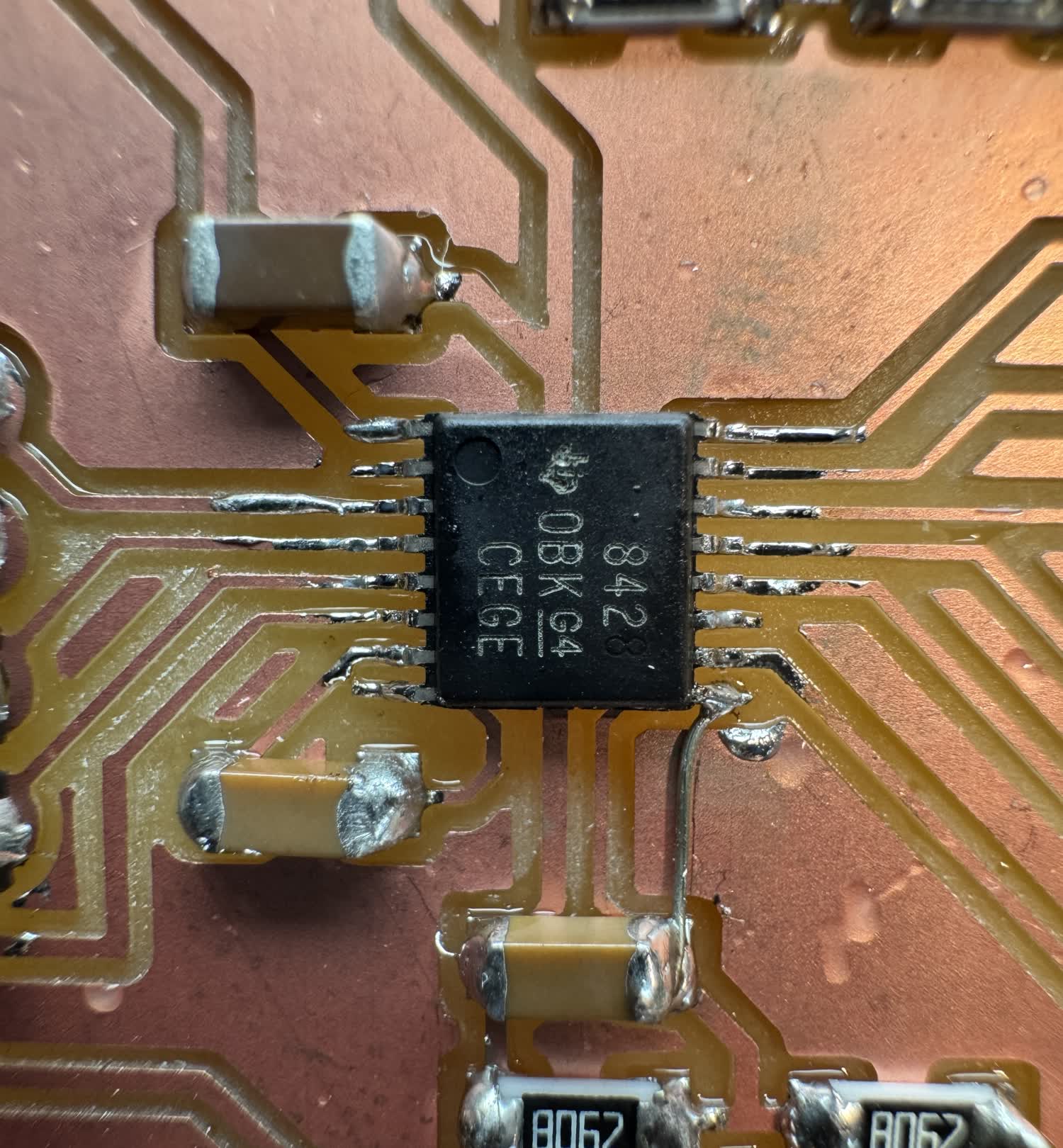
Regarding the soldering of the drivers, he suggested three different methods. I could use solder paste which was what I was originally planning on doing. I could
use a fine tipped iron and just do it by hand, one trace at a time. Or, I could make a giant glob of solder across all of the traces and then wick away the excess
after the component had been attached.
To make sure my Pico W was working, I orignially was trying to blink the onboard LED without any success. Anthony confirmed what I had seen online, the LED wasn't
connected to the actual RP2040 but rather the other MCU (I believe the Wi-Fi chip) on board the controller and I couldn't figure out how exactly to connect to it.
He suggested a far simpler and more reliable option which was simply to print to Serial which worked and confirmed that the board was infact working.
As for dealing with the traces. If I wanted to move forward with the board that I had, he recommended fully removing the broken traces and connecting the driver
to the pads that existed and then using additional wires to jump the broken traces. He also suggested that I try milling the PCB one more time except where I
decrease the cut depth into the material from the standard 4 mil to 2 mil. It turns out that the 4 mil standard is around three times deeper than it needs to be
and he thought that by reduing the depth of cut would reduce how delicate the traces were and hopefully enable them to stay.
After my meeting with Anthony, I decided to try and mill the board one more time with that shallower depth of cut to see if it would work. It didn't... Surprisingly, it actually turned out worse than the second attempt that I had done. I still am really surprised by that and wonder if the endmill wasn't the best even though Gert and I inspected it under the microscope in advance. I want to try it again just to confirm. I did unfortunatley forget to take a picture of it though. Even though the third attempt failed, it provided a great board to practice soldering on and test which method I would want to use for the drivers.
Soldering
The first thing that I wanted to do was to test the soldering methods that I discussed with Anthony to see how I should solder the drivers.
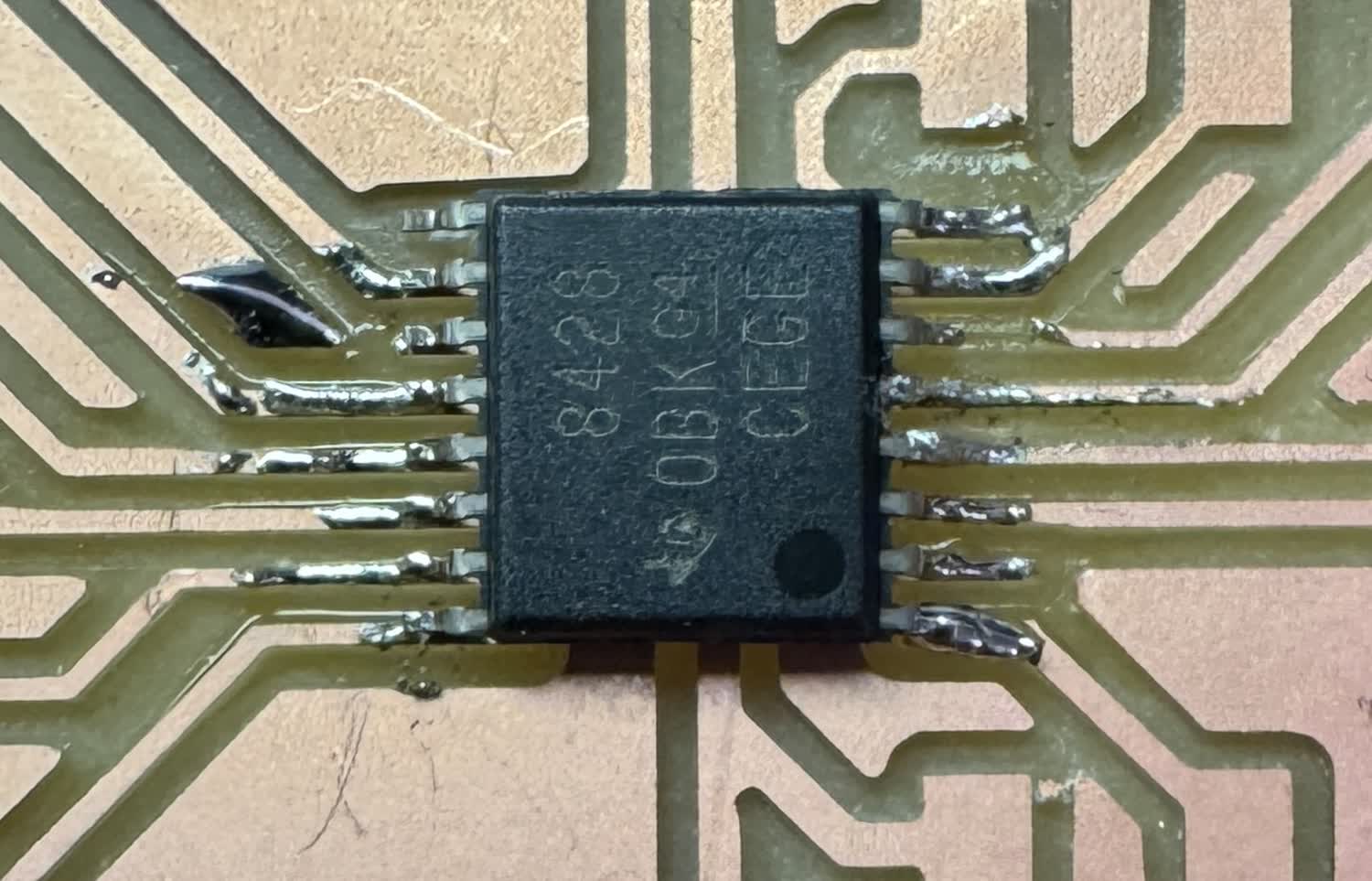
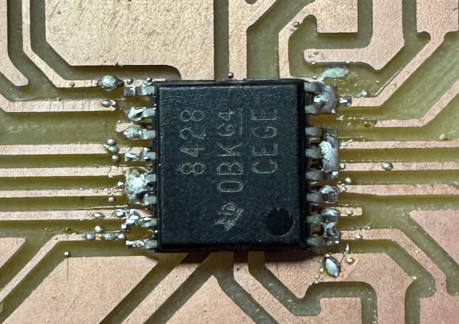
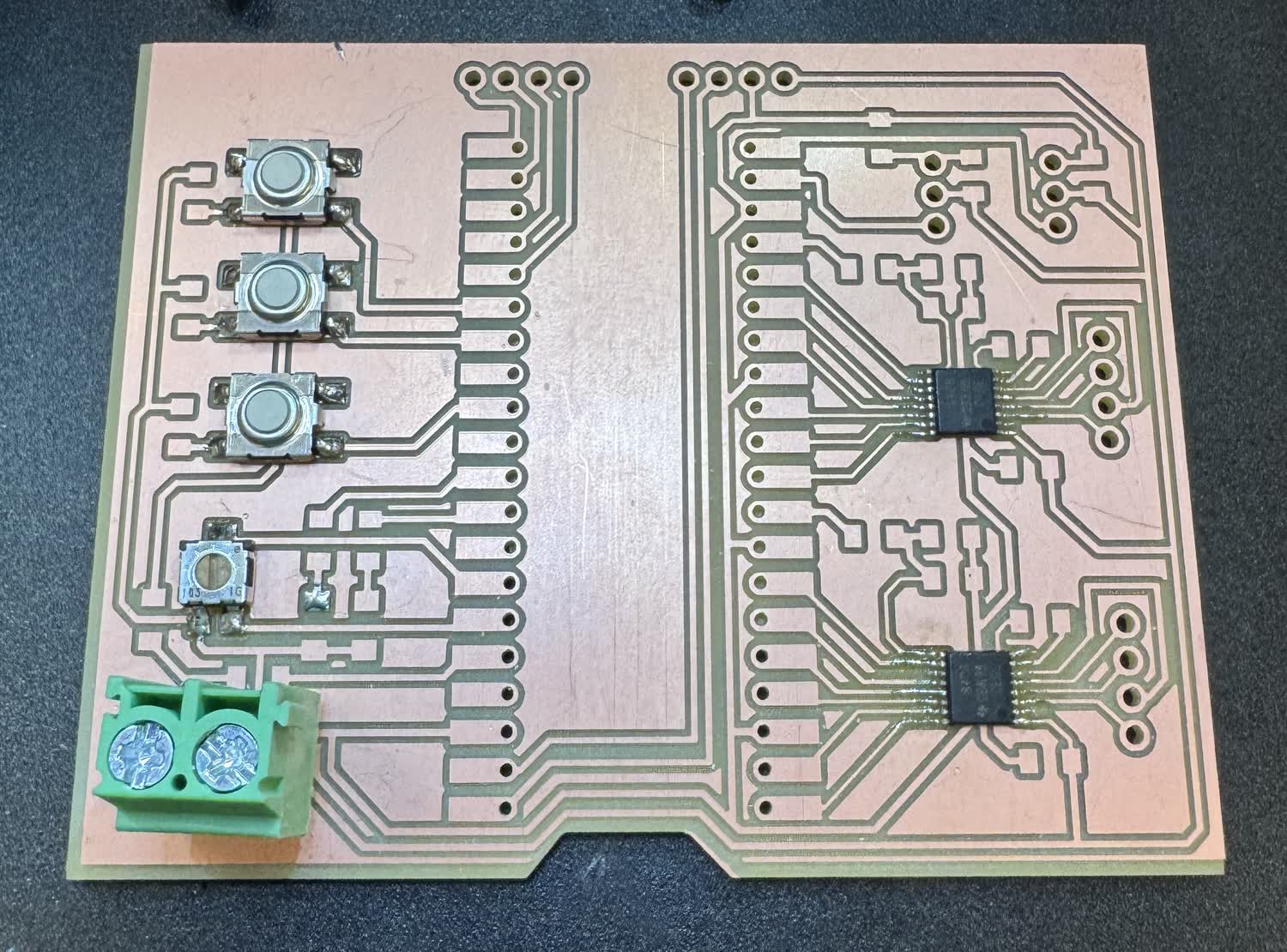
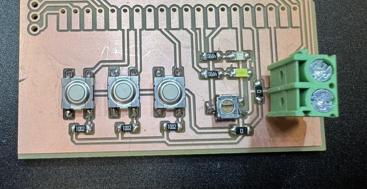
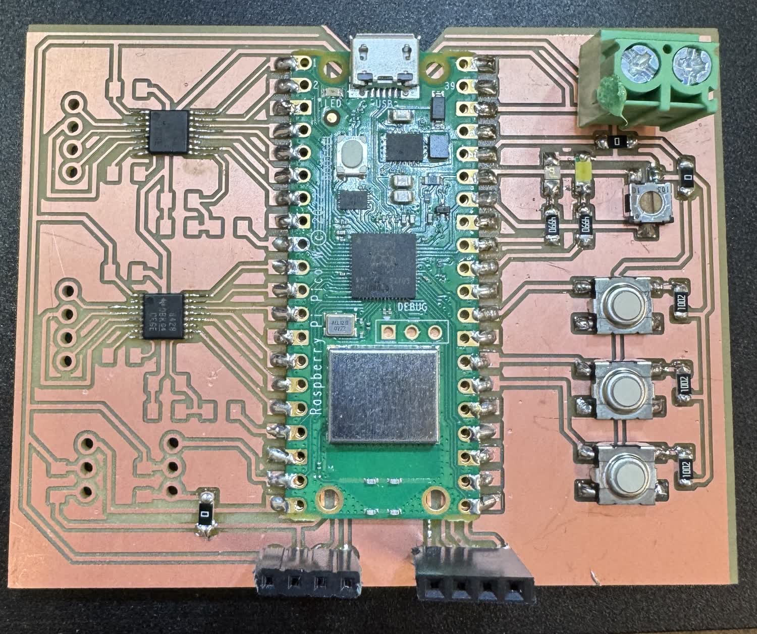
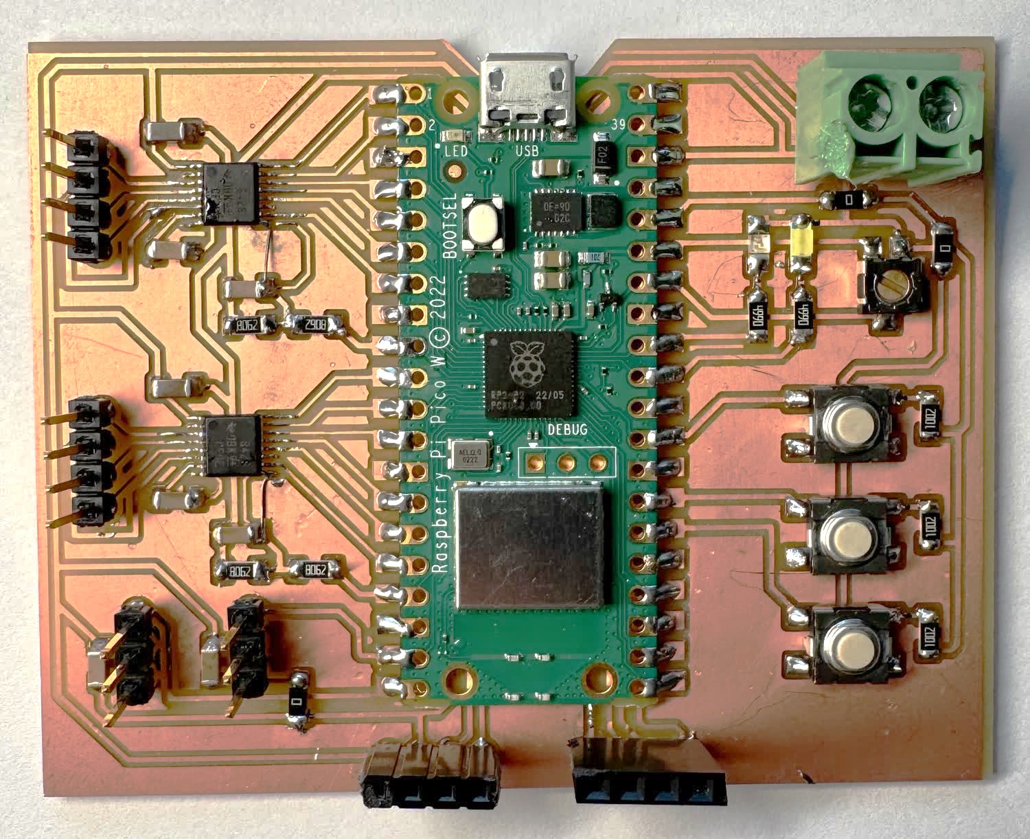
With that testing completed, I began soldering the drviers on to the final board. My plan was to solder what I could on the drivers, then the rest of the components,
and then make the neccesary jumps from the driver to the other locations as neccesary. Regarding the components that I soldered ie. resistor and capacitor selections.
I used a 499 ohm resistor for the LEDs, 10k ohm resistors for the buttons, a few 0 ohm resistors, two 1 microfarad capacitors for V_motor and then six 0.1 microfarad
capacitors for other stabilization. For the resistor set up for the Vref pins, I used four 80k ohm resistors. Below are images showing the progression of the soldering.
Testing
Unfortunatley, I don't have any video or image proof as I ran out of time and it was three o'clock in the morning, however, I incrementally tested each component on the board
and the only thing that hasn't worked so far is the drivers themselves which I would consider an amazing result! I don't think I have functioning code yet for them so I am not
ready to say that it is an issue with the board. Which leads to one of the biggest mistakes I made this week. It took me until Wednesday at 3:20 in the morning, the
day this was all due to look the component up on the class website! I don't know why I was surprised but I found a perfectly fine example of a PCB and code to test the DRV8428.
ARE YOU F****NG SH***NG ME! Needless to say, I feel an imense amount of frustration even as I'm writing this. This serves as a very valuable lesson though! So many of my troubles the past two
weeks could have been solved and I could have probably saved six hours if I simply looked on the website.
Thoughts and Reflection
What is most likley going to happen is that I will go ahead and test my drivers with the code from Neil on the class website and see if they work. When they likely do not work, I am going to redesign the PCB and model it after Neils on the website. I might also try and shrink the form factor a little bit more. I might also send it out to get manufactured.Despite all of the frustration I encountered this week, I am actually incredibly pleased with the result. I was expecting most of the board to fail and yet almost everything worked! I definitley learned a lot about the PCB millling machine and the process as a whole and feel quite comfortable with it which was the goal of the week. I have gone back and fourth on whether or not the board that I tried to make this week was too complicated for a first attempt but now that it is all said and done I think it was a great idea. I threw myself in the deepend and pushed the limits of the machine as well as my knowledge and learned a ton as a result. Even though part of the board doesn't work, I gained a ton of experience, have a plan of how to go about and fix it, and am comfortable enough with the programs and machines neccesary to execute it. I couldn't ask for more than that. I think the most important thing I learned this week is that when using a "new" component, look it up on the class website, it is almost certainley not new. Someone has likley used it before and there is likley documentation for how to work with it. Again, had I done this earlier with the driver, I could have saved myself hours of frustration and likley had a fully functioning final board. By not looking it up though, I learned a ton through pouring over a data sheet and trying to design a schematic myself which will be helpful in the long run. I do not think that this week is complete. I want to test and likely fix my stepper drivers, and will likely have to make a new PCB, I also want to add the code that I used to test the PCB. I also need to add the work for the group assignment. I just have to stop working on the project for the day as I have an exam tonight that I have to study for.