![[Profile Image Placeholder]](profile.jpg)
Week 13
Wildcard Week
Week Highlights
Key captures from the wildcare week assignment, combining fiber laser circuit engraving with UV laser glass engraving, each linked to their sections.
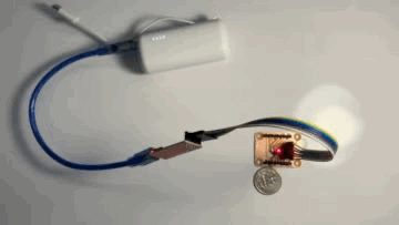
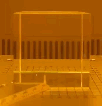
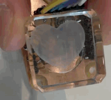
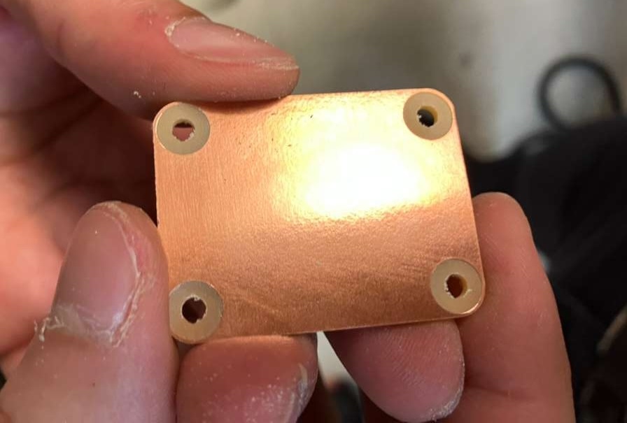
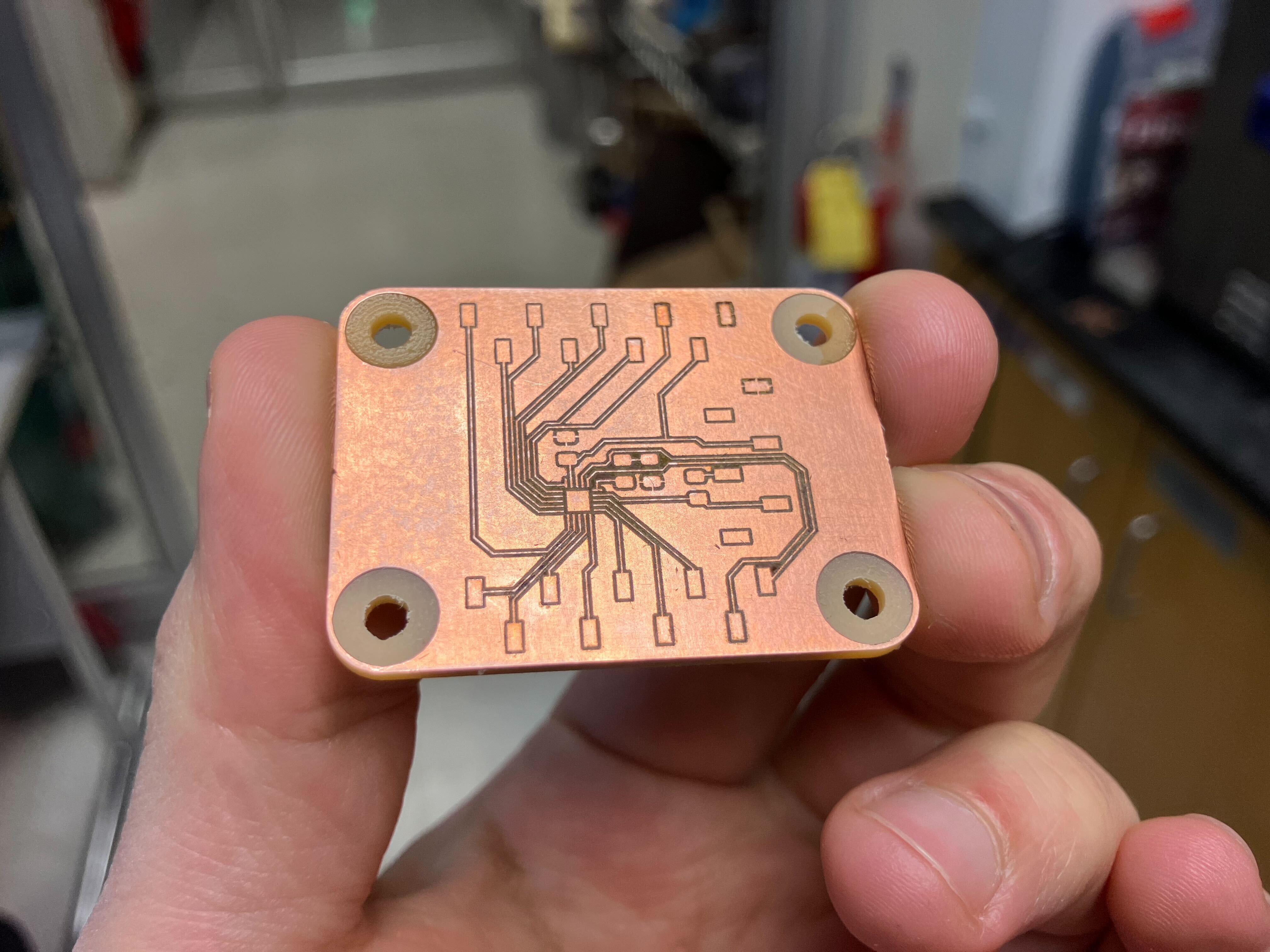
Table of Contents
Course Content
Training & Documentation
Wildcard Week
This week focuses on exploring digital fabrication processes not covered in previous assignments. We'll design and produce something using computer-aided design and manufacturing, documenting requirements and including everything necessary for reproduction. This week also includes reflection on the impact and purpose of making (almost) anything.
This Week's Goals
- Explore New Processes
Design and produce something with a digital process not covered in other assignments - Complete Documentation
Document requirements and include everything necessary to reproduce the project - Reflect on Impact
Understand the purpose and impact of fabrication labs and making
Assignments
- Wildcard Assignments
Design and produce something with a digital process (incorporating computer-aided design and manufacturing) not covered in another assignment - Assignment
Design and produce something with a digital process (incorporating computer-aided design and manufacturing) not covered in another assignment, documenting the requirements that your assignment meets, and including everything necessary to reproduce it
Tools & Materials
- Carvera (CNC Mill) — Edge cuts and hole machining
- Fiber Laser Cutter (xTool F2 Ultra) — PCB engraving
- PCB Design Software (KiCad) — Board layout and design
- ATtiny1626 Microcontroller — Target device for development board
- RP2354A Microcontroller — Complex board design
Lecture Notes
Week 13 lecture covering major announcements, week 12 review, system integration reminders, and wildcard week preview.
Theme of the Week
'Step away from the panic'
Major Announcements
- Subject evaluation: Required for funding the class. Provides feedback to the institute about the class. Important for future students if you care about successors in the class.
- Calendar alarm: Wildcard week and recitation on why make (almost) anything: impact. Friday is cutoff for assignments and orders (10s of dollars per person from inventory).
- Final presentation/final exam: Combining multiple additive and subtractive processes (not just design a board and 3D print a case). Goal is system integration out of parts. Final exam criteria:
- Did you integrate and design a complete system?
- Can you demo a final project? Here is the cool thing I did and here is how it works.
- Make a final project video! (helps but not required)
Review of Week 12 User Interfaces
- Claire Wang: Music play and Windows 3.1 interface works!
- Ryan Hoffman: DRV8251A discussion, heat sinks, breakout boards. Wildcards with waterjetting, EDM, multi-axis machining, laser cutting metal. Class in the spring on nature of mathematical modeling.
- Srikanth Nadhamuni: Background and experience to visiting fellow at MIT. Raspberry Pi W for WiFi, n8n for cloud LLM data crunching. Software: Node.js, MCP bridge server with n8n based on bridge connected to device (NGV tunnel). All set! Fantastic experience, haven't worked so hard in a very long time and learning a lot of new things. Hope to take forward and build other systems. The whole culture of doing and trying yourself fascinating, especially with failing a number of times until you figure it out. Maybe set one up at an IIT in India or AI centers of excellence with education ministry into the Indian education system (see fablabkerala.in or vigyam ashram).
- Ray Song: Not here.
- Tyler Jensen (Lincoln Lab, Group 81): Final project discussion (nylon printer). Week 13: Easy for web serial interface for XIAO! Web server to TFT (I think I forgot to load the camera pins with my code for it).
- Aditi Ramakrishnan: Sloan MBA and strategy consulting background. Discrete time filter (FFT is blown) in skimage.filters — make a bandpass filter, then run a series of these filters, much less computing only adds and multiplies for filtering in realtime.
- Alexandros Gravalos: Not here.
- Edward Chen: Check final watch project by Gulati into watch form factor. Clear print on the Form Labs printer, 0.1. Kaman filter for sensor fusion (in the spring class). For position — LSM6DSV16X from input devices. Acceleration at 7 kHz (at audio frequency).
Show and Tell
- Handle to sensor WiFi user interface
- Plug to audio LLM user interface
System Integration Reminders
- Mount electronics
- Strain relief the final projects
Preview for Wildcard Week
Assignment: Design and produce something with a digital process (incorporating computer-aided design and manufacturing) not covered in another assignment.
Recitation Notes: Why Make (Almost) Anything
Recitation exploring the purpose, impact, and scaling of fabrication labs and making infrastructure.
Map of Fab Labs
Why Make a Fab Lab?
- Used to create a community
- Building things for the community
- Sustainability
- Prototyping quickly
How Impact?
- How to make spaces: How to measure impact. What is important about fab:
- Fablabs in cities vs rural areas: The ability to decide their own futures and change their lives fundamentally. 'Safecast revolutionized citizen science' e.g. radiation map.
- Bringing back manufacturing: Reducing reliance on supply chains.
- Rural sustainability: Working with indigenous communities on creating technologies themselves at scale and measure their usefulness and efficacy to preserve their ancestral knowledge:
- How to establish labs there
- How to make sure the labs get used
- Hygiene technologies with Proctor and Gamble: Highly commercial. Lots of plastic waste. How can we change how they produce? How to make their products get there through resellers?
- Trip to Peru and ran workshops, questionnaires, analysis: Collaboration developed into how to produce the products but also how to test their products to be market valuable e.g. mosquito repellents. Out of three plants, two worked better and one wasn't working at all (which is important to know!).
What Does It Mean to Design Infrastructure?
- What did we want this lab to be able to do?
- Workshops and questionnaires
- How much you educate people based on the info they have with the issues the community is facing
- Energy concerns to consider, some machines just drain the grid and can't be used. Solar powered, battery powered machines, reducing energy consumption of machines. Many concerns important.
- Ethical questions
- How to maintain resources
Case Study: Water Purifier Packets
Use them, change them, source them locally, ingredients found locally, how to distribute them globally.
Funding Models
First few fablabs were NSF funded. Now corporate CSR, regional funding, labor funding (10 different ways). Successful fablabs are heterogeneous with lots of ways of funding. The ones that fail usually just have one sponsor.
Example: DIY Raman spectrometer for water purification (even after purifications still have sulfates and improving that too).
What Does It Mean to Scale Infrastructure?
(Besides a lot of meetings!) What is a reasonable way to design a data collection process about what is needed and how to achieve it.
Back to the Map: Expansion
Timeline of development, cocreation, portable, skin analysis, water testing, biomaterial tech, microscopy.
Initial Results from Boston
How to Confront Local Impact
- Collab with University of Hamburg. Motivation for how much food can be produced in Boston. Where food waste goes and what Boston produces locally. Make things for yourself locally.
- Impact directly in the community you're living in.
Hatchspace
Focused on rehabilitation of addicts with woodworking. (Vermont is wood producing state).
Example Course Program
- All-in session and systemic impact
- Natural and cultural context
- Skills and workshop
- Economic vitality
- Skills and workshop
- Co-work session
- Solutionspalooza
In the Course
Hands-on component (no physical robot exists that can do it) and community component is also important. Inclusion is important. Solving unconscious and institutional biases.
- 'Fabrica! Lab' — Creating new laboratory spaces for female high school students, courses aimed for women in technology, online advising sessions for females interested in tech.
- Makerspaces — Access to tools behind closed doors at universities, makes a huge difference for people who don't have the ability to prototype for themselves.
- Materiom — Fablab affiliated project on organic waste for biomaterials.
- Fablab León
- Skylab workshop experiment — How to run a noodle shop out of a fablab (creating food from the community).
- Academany — Global distributed campus for high school education. Fablab all-in (belonging, impact, community), fab futures (future vocational skills), bio academy (synthetic biology), fabricademy (textiles, fab, bio), fab academy (digital fab apps and implications).
Trade-off Between Impactful and Dangerous
People could be doing bad, but not because doing it with a group people with values.
Questions
Clarification: Adding infrastructure to existing fablab infrastructure to help support specific community needs (not specialized fab labs).
Foundations for Fab Futures
July 27-31, 2026 at Fab Boston 2026.
Useful Documentation
Essential resources for wildcard week digital fabrication processes and PCB design.
Class Page
Comprehensive resource covering wildcard week assignment requirements and possibilities including grinding, multi-axis machining, electrical discharge machining, waterjet cutting, flatbed cutting, plasma cutting, laser metal cutting, laser micromachining, welding, molding and casting, folding, robotics, electronics, embedded programming, food, materials, biotechnology, textiles, and composites.
Key Topics
- Machining: Grinding, multi-axis machining, electrical discharge machining, waterjet cutting, plasma cutting, laser metal cutting, laser micromachining
- Molding & Casting: Vacuum forming, rotocasting
- Folding: Mathematics, form and function, kirigami
- Robotics: Arms, construction, soft actuation pneumatic inflatable
- Electronics: Pick and place, programmable logic
- Embedded Programming: Machine learning, machine vision
- Textiles: Fiber processes, knitting, embroidery (PEmbroider, Ink/Stitch), Fabricademy
- Composites: Various composite fabrication techniques
ATtiny1626 Development Board References
- ATtiny1624-26-27 DataSheet (DS40002234A) — Official Microchip datasheet for ATtiny1624, ATtiny1626, and ATtiny1627 microcontrollers
- Tindie: ATtiny1626 Development Board — Commercial development board reference and pinout information
- AVR Freaks: ATtiny1626 Discussion — Community forum discussion on ATtiny1626 development
Embedded Programming Course Resources
Course resources for embedded programming with ATtiny412 microcontroller examples:
Embedded Programming - MIT Academy
- t412-blink-4: Pin pro, sch, pcb, board, components, traces, interior, blink.ino
- t412-blink-3: Pin board, components, traces, mask, traces+exterior, interior, blink.ino, blink.c, make, video
- t412-blink-2: Pin board, components, traces, traces+exterior, interior, blink.ino, video, ring.ino
- t412-echo: Board, components, traces, traces+exterior, interior, echo.ino, video, echo.c, echo.make, video
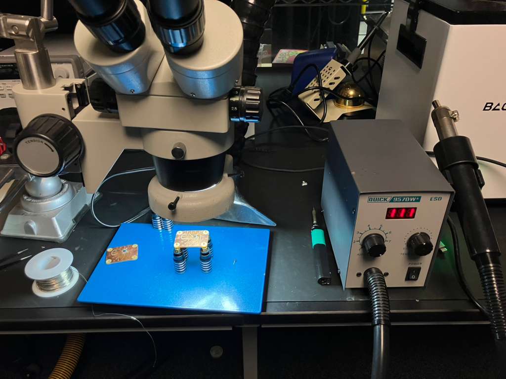
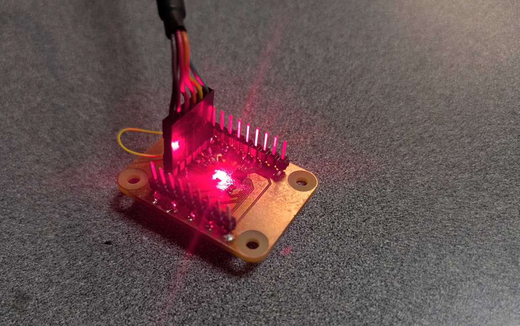
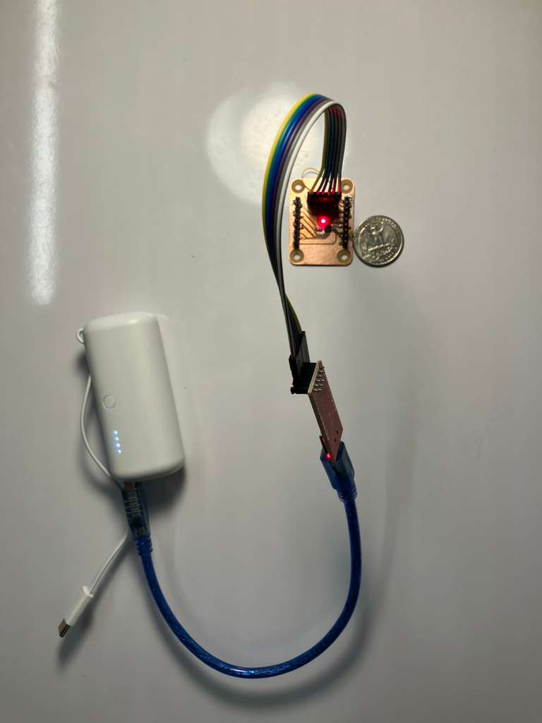
Assignment: PCB Engraving with Fiber Laser
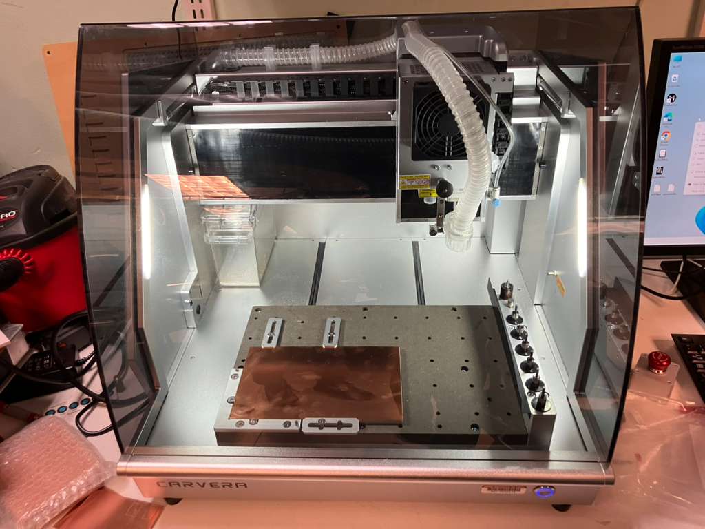
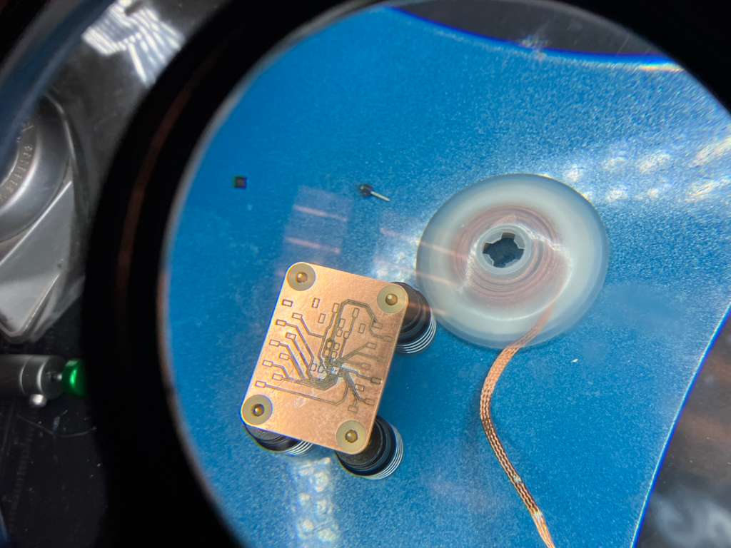
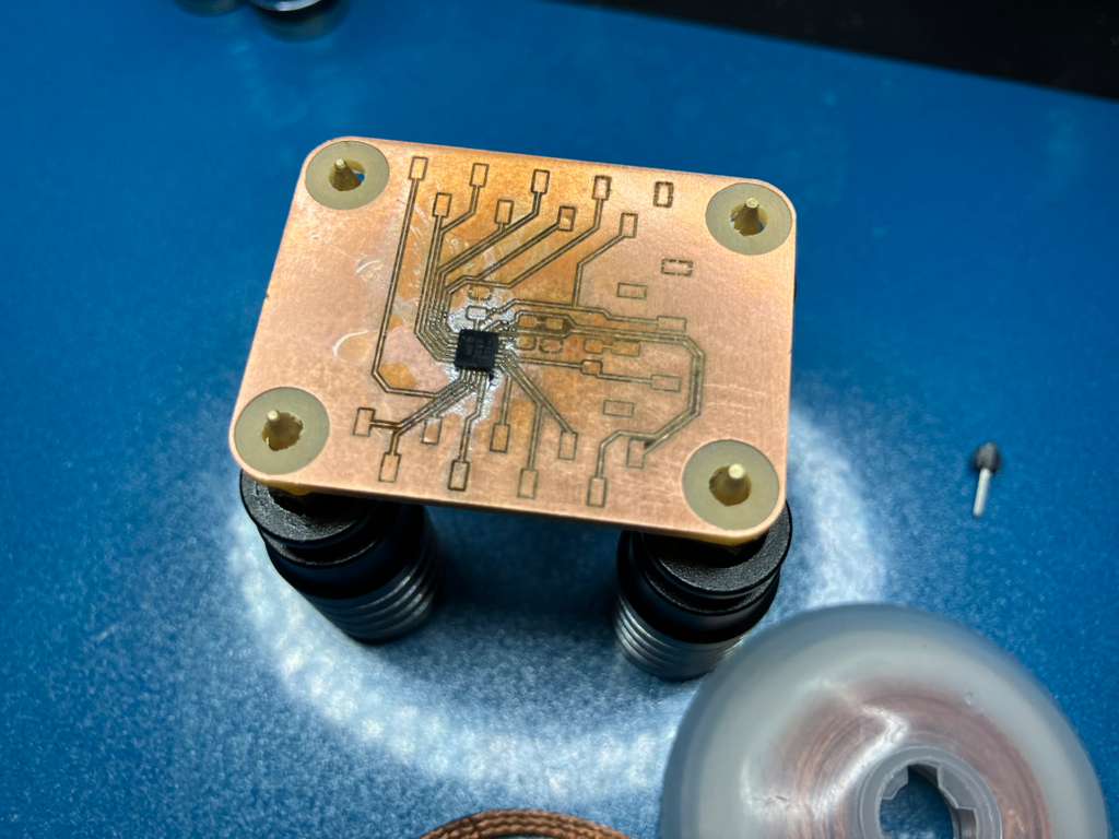
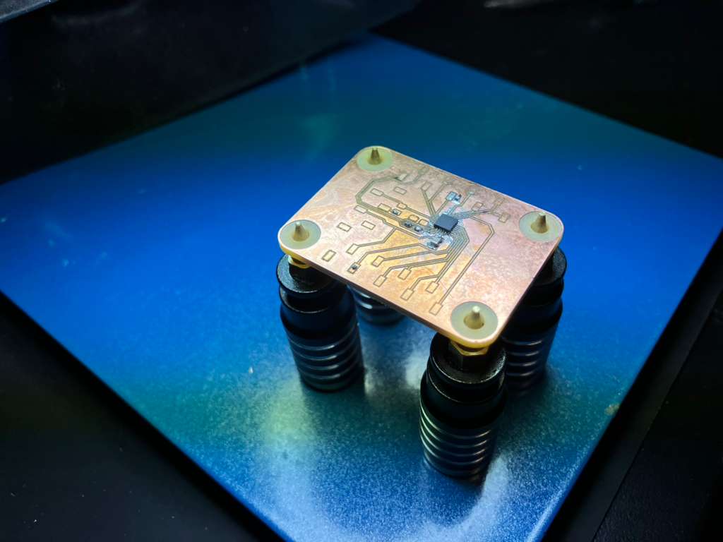
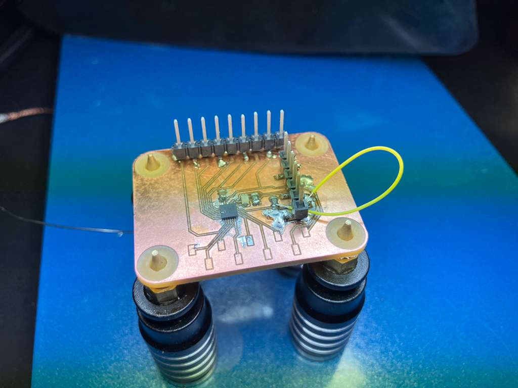
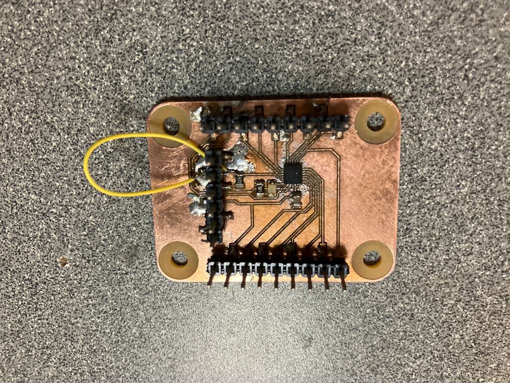
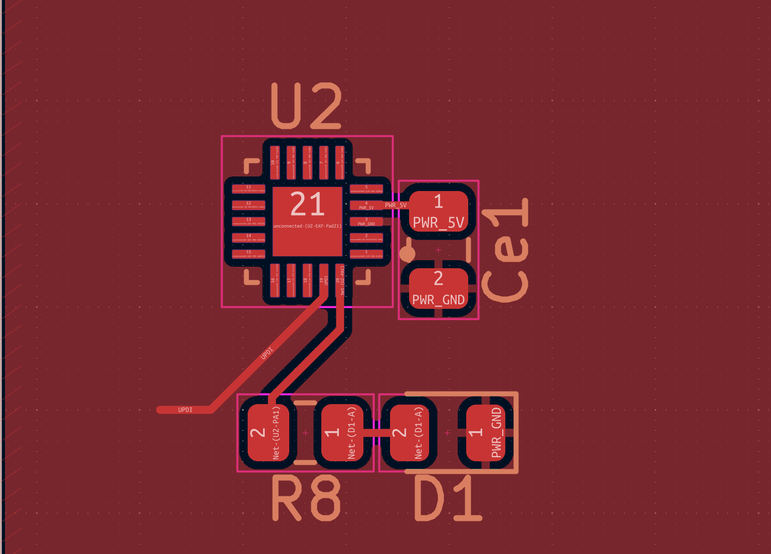
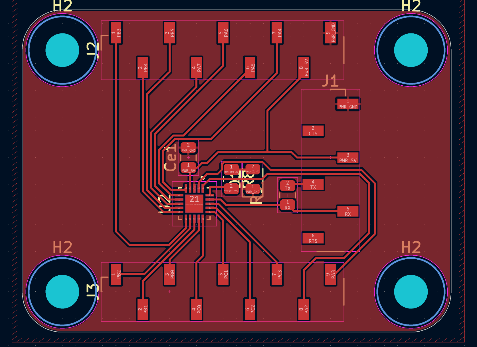
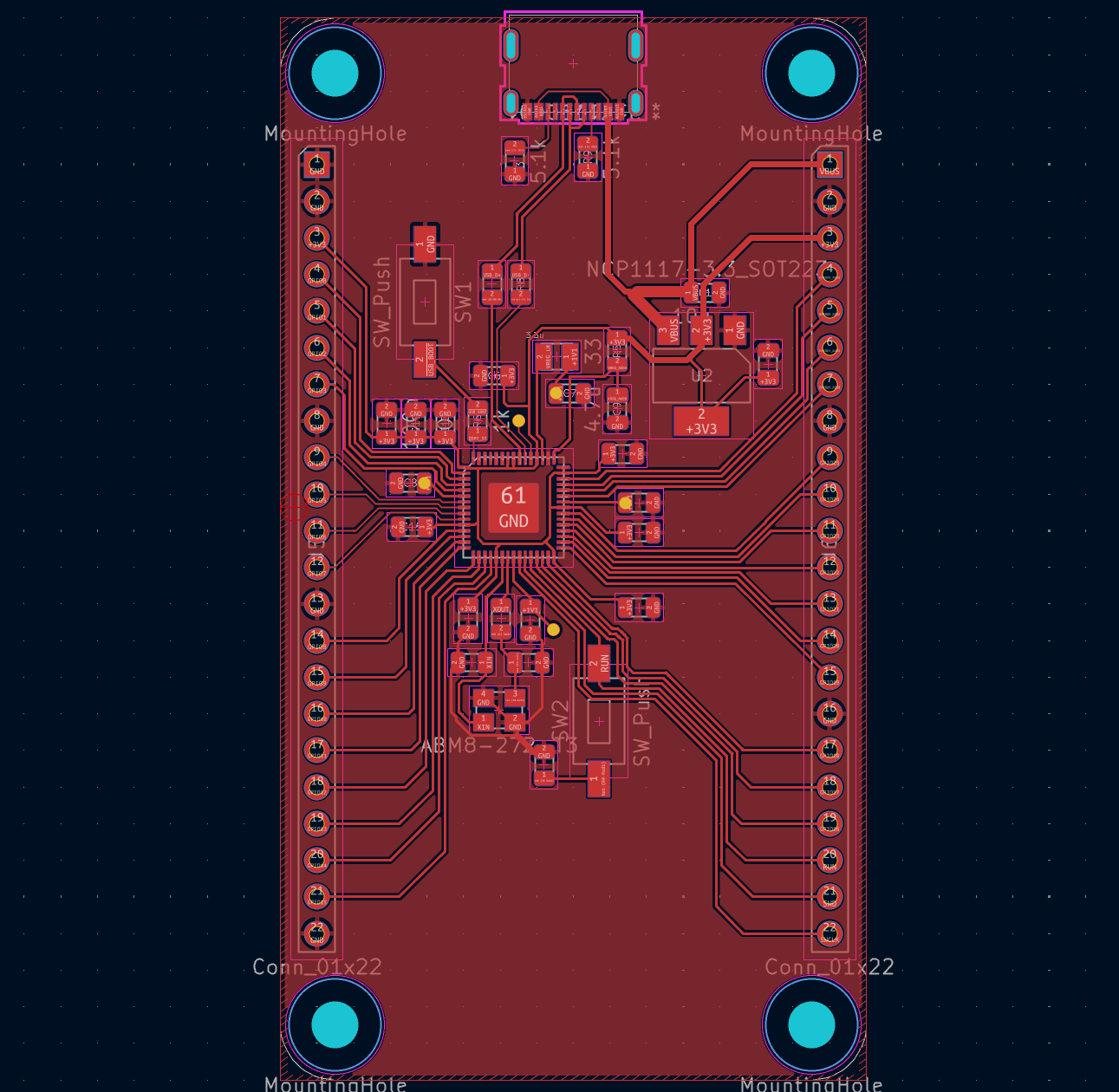
Design and produce something with a digital process (incorporating computer-aided design and manufacturing) not covered in another assignment. This assignment demonstrates PCB design and fabrication using a combination of CNC milling (Carvera) for edge cuts and hole machining, and fiber laser engraving (xTool F2 Ultra) for trace creation on copper-clad boards. The project includes designing and fabricating two development boards: a simple ATtiny1626 development board and a complex RP2354A development board.
PCB Engraving Process
This project explores PCB fabrication using fiber laser engraving, a process not covered in previous assignments. The workflow combines subtractive manufacturing techniques: CNC milling for mechanical features (edge cuts and holes) and laser engraving for electrical traces. This approach enables rapid prototyping of custom PCBs without requiring chemical etching or specialized PCB manufacturing facilities.
Tools and Equipment
- Carvera (CNC Mill): Used for edge cuts and hole machining. The laser cannot effectively cut through the board material, so mechanical cutting is required for board outline and mounting holes.
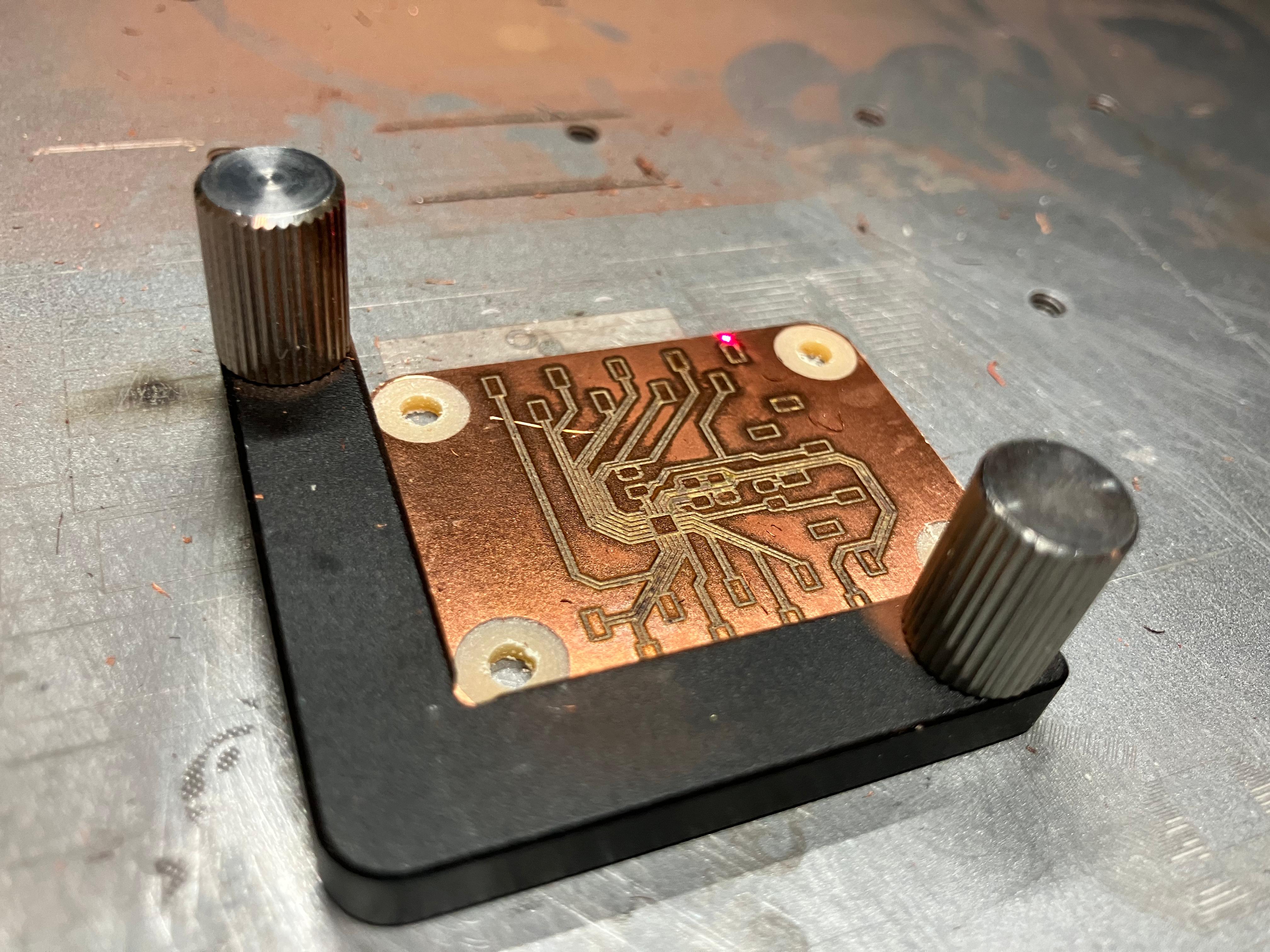
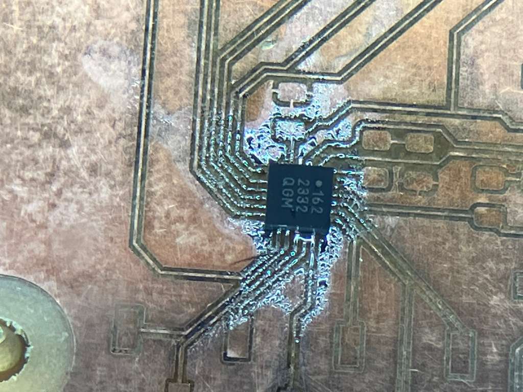
- Fiber Laser Cutter (xTool F2 Ultra): Used for PCB trace engraving. The laser removes copper from the board surface to create electrical traces and pads.
- PCB Design Software (KiCad): Used for schematic capture, PCB layout, and design rule checking.
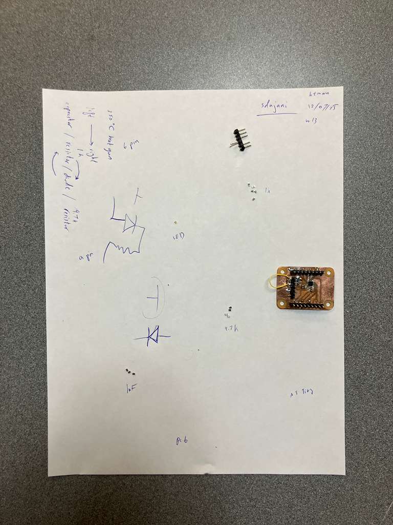
Boards Designed
- Simple Board: ATtiny1626 development board with connectors, resistors, LED, and capacitor
- Complex Board: RP2354A development board with more advanced routing and component placement
Board Design Considerations
- Connector Placement: Top and bottom for connectors, right side for flashing. Connectors along edges to minimize form factor and maximize space usage.
- Vertical Connectors: Used instead of horizontal connectors because horizontal connectors risk being snapped during use.
- Black Area Avoidance: Avoid large black areas because laser does not work well with that (keep traces closer and further to minimize black areas). Note: Need to characterize maximum black until it burns the board because dumping too much heat in one place can damage the board.
- Breadboard Compatibility: Put connectors on 100mil spacing grid size for breadboardability.
- Pin Count Adjustment: Missed six pins in initial design, so switched from 6-pin headers to 9-pin (distributed six on top and bottom).
- I2C Resistors: No SDA or SCL resistors included to keep flexibility for future use. May add spot for zero-ohm or pull-up resistor later but keeping it simple for now.
- Mounting Holes: Added aligned mounting holes (M3 usually — for 3mm screws) for mechanical mounting.
- Rounded Edge Cuts: Do 90 degrees, copy, drag, and complete the shape for rounded corners.
Design Rules
- 0.1 mm spacing minimum
- 0.15 mm trace width minimum
- 0.15 mm clearance between plane and the rest
Ports and Pins
ATtiny1626 is an 8-bit microcontroller with 8 pins maximum per port. Each port has 8 pins maximum (some less). Need to specify port letter and pin number:
- PA (0-7)
- PB (0-7)
- PC (0-7)
Postprocessing
- For Carvera: Add new layer with just the holes in Photoshop (only holes for machining).
- For Laser Engraving: Get rid of the holes for the F2 tools engraving in Inkscape (the frame and the board for alignment, then only engrave the board, not the edges).
Carvera Machining
Using mods → mill 2D PCB workflow:
- 0.12mm cut depth and max depth
PCB Engraving Process
Using xTool F2 Ultra fiber laser:
- Use tape for laser alignment
- Run a test first on spare copper before the Carvera cut board to make sure focus is good (2.7mm thickness setting worked, board is actually 1.6-1.7mm thick)
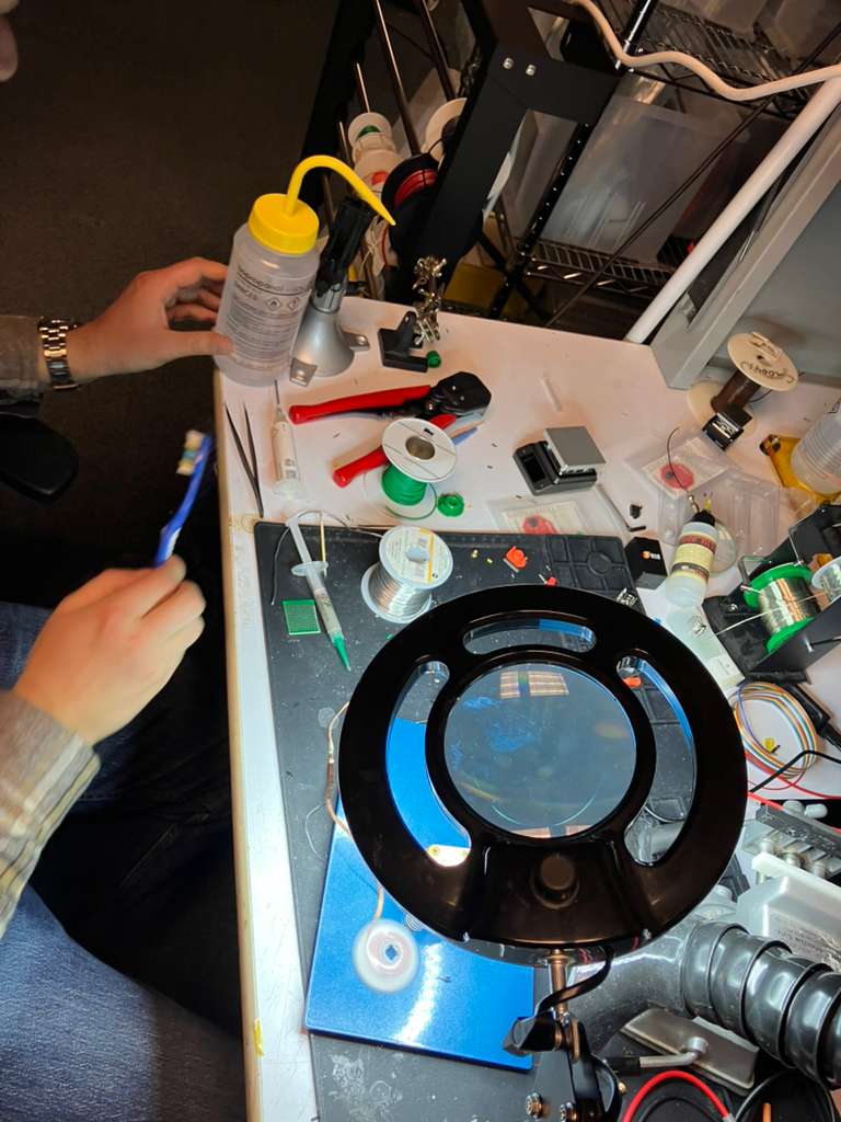
- Sand after engraving to clean up any residue
- Worked with Bantam Tools FR1 (not random Amazon copper)
- Perform short circuit test after engraving
Soldering
Using solder gun (heat gun) for component assembly.
Components
- 1x 6-pin flipflop headers
- 2x 9-pin flipflop headers
- 1x 4.7k resistor
- 1x 1k resistor
- 1x LED
- 1x 1uF or 10uF capacitor
Design Files
Download design files: ATtiny_QFN.zip and RP2354A-dev-v1.1.zip
Process Documentation


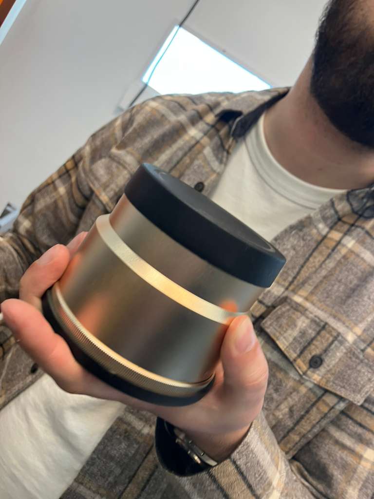
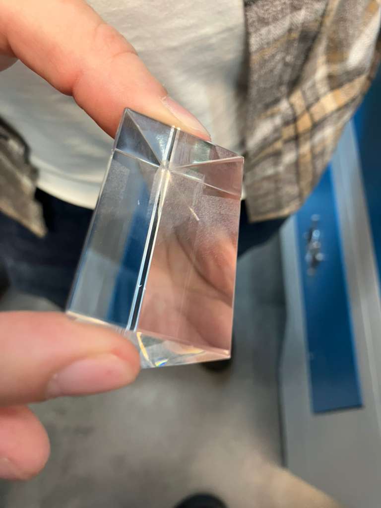
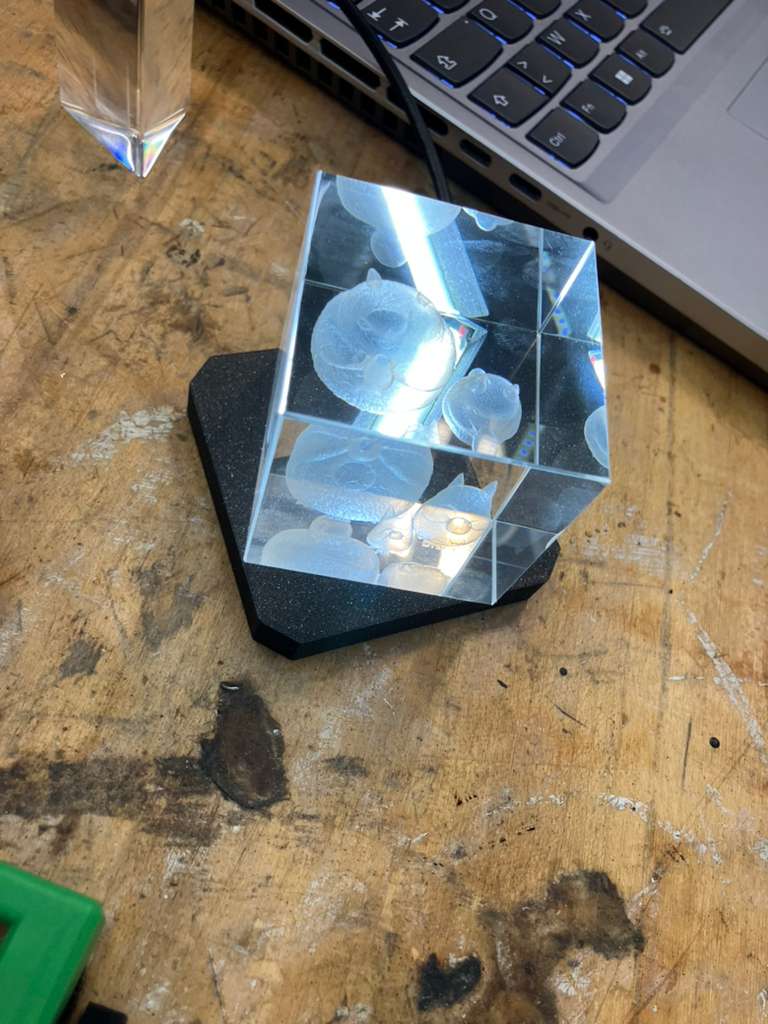
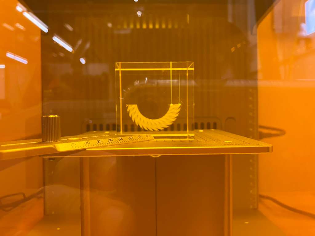
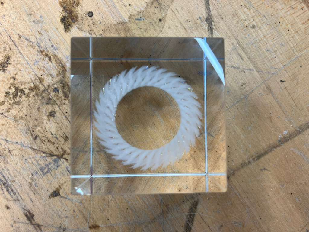
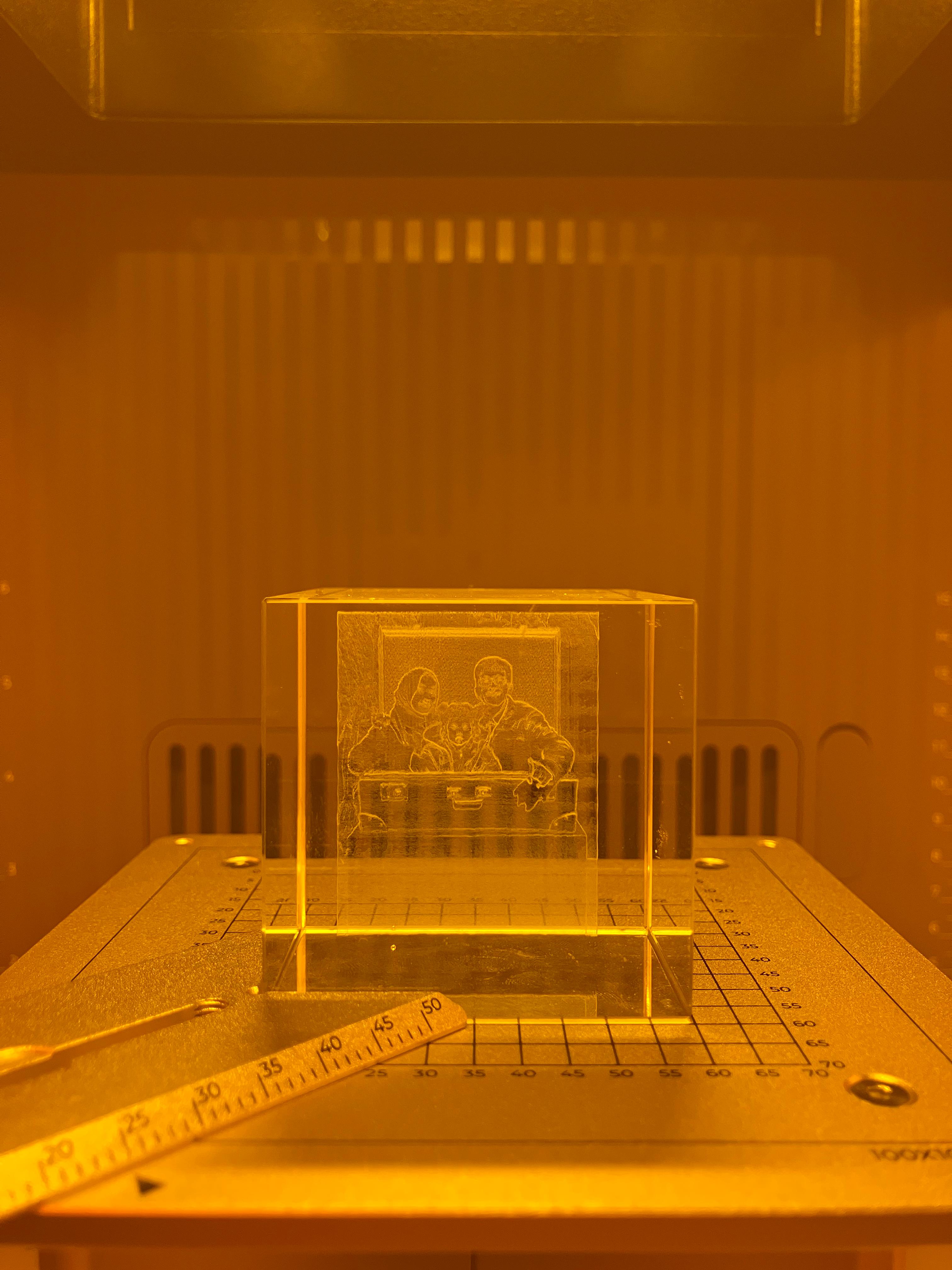
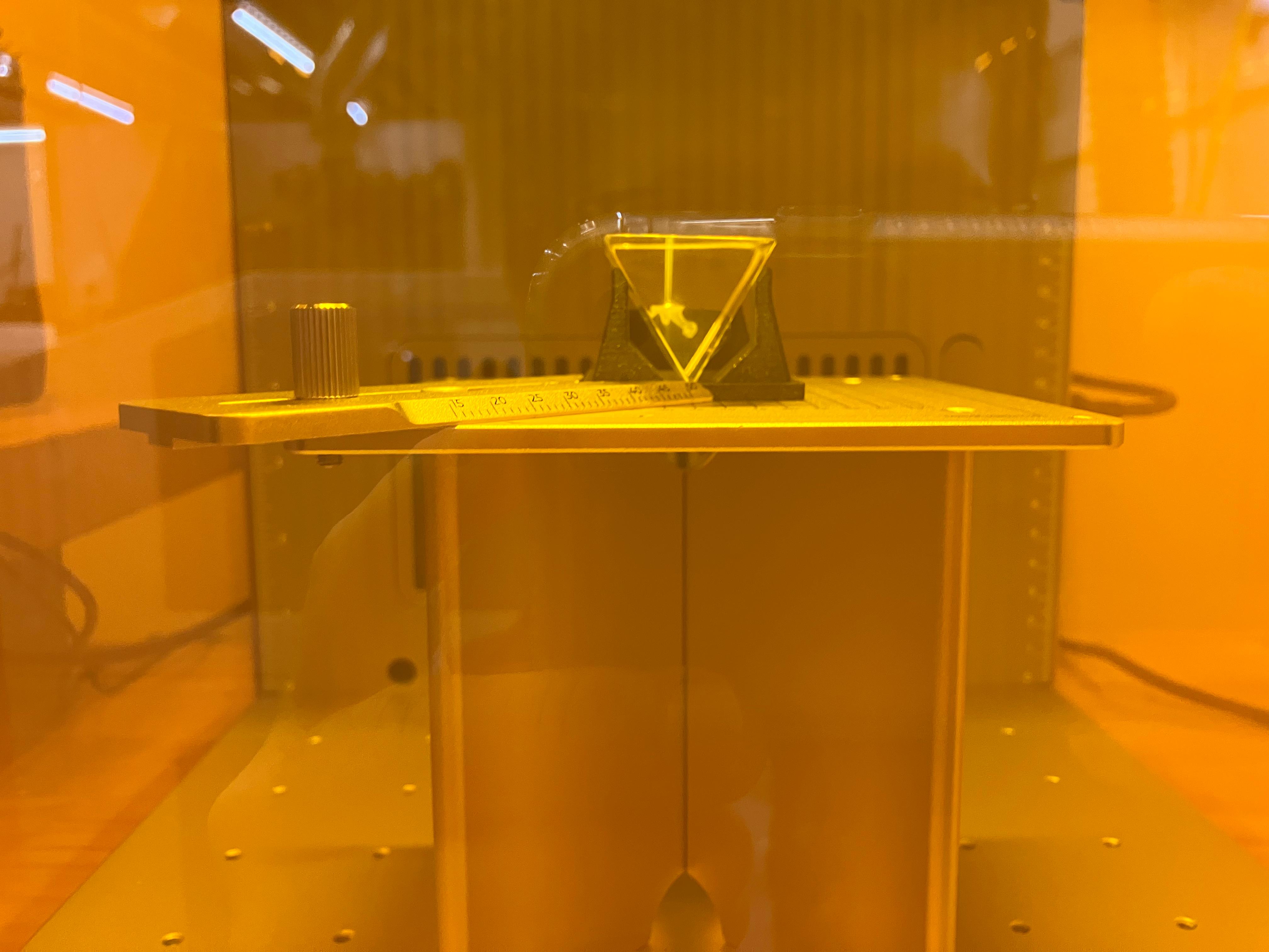
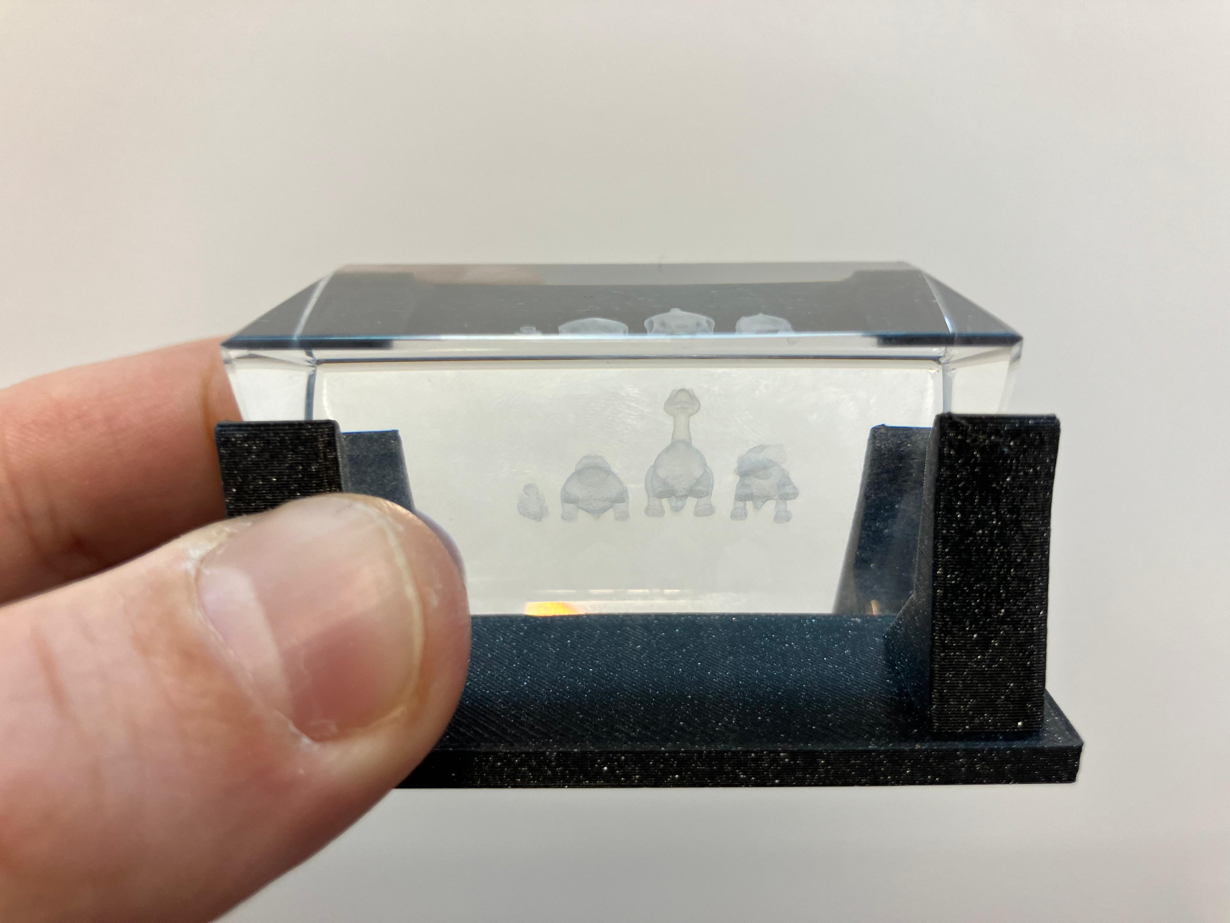
Assignment: Glass Engraving with UV Laser
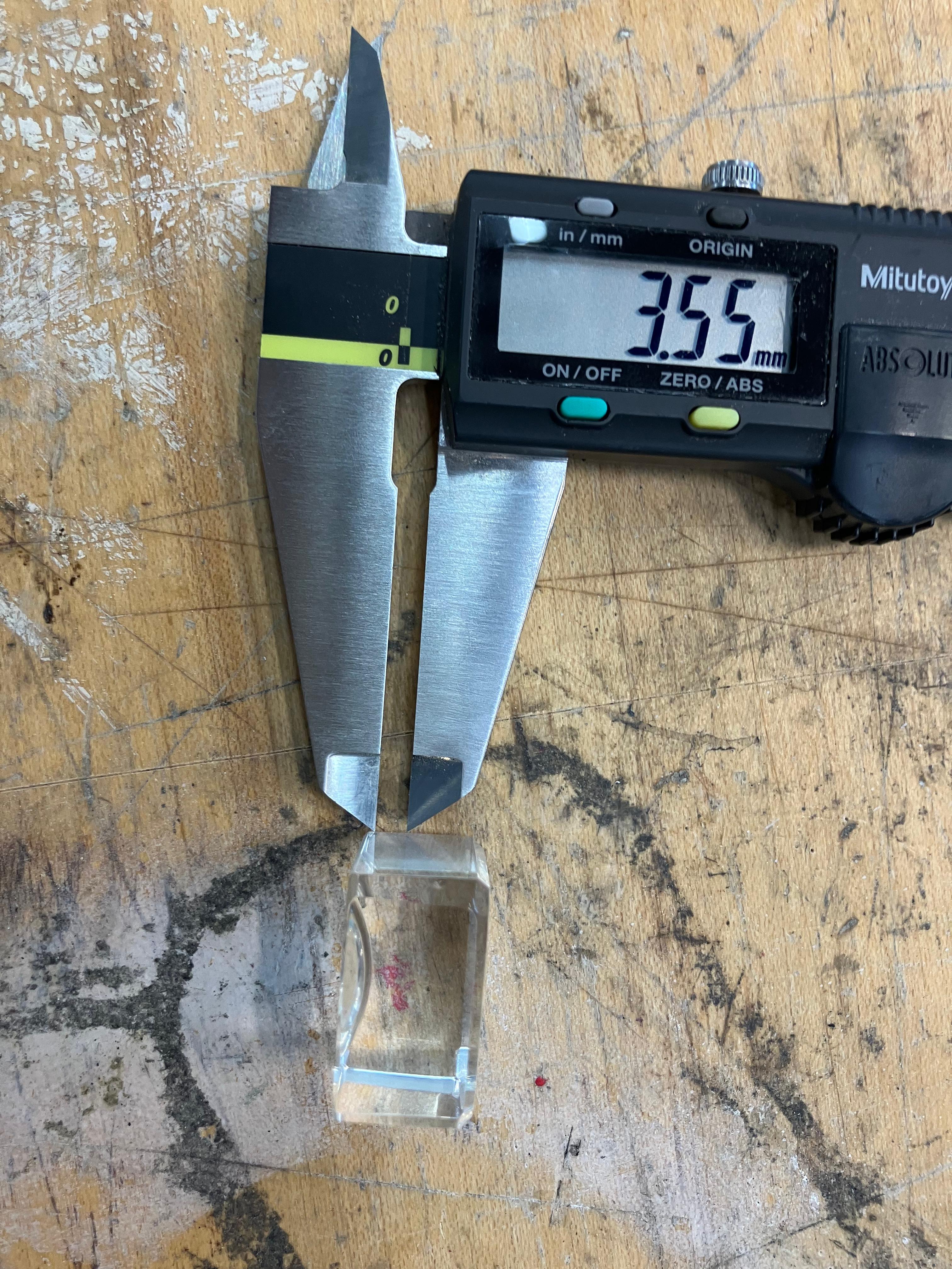
Design and produce something with a digital process (incorporating computer-aided design and manufacturing) not covered in another assignment. This assignment demonstrates glass engraving using UV laser technology to create volumetric engravings in K9 glass, enabling both surface and volume engraving techniques with different focal length lenses.
Glass Engraving Process
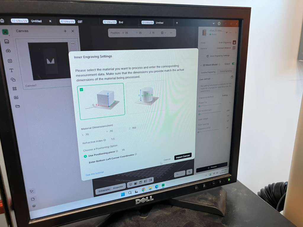
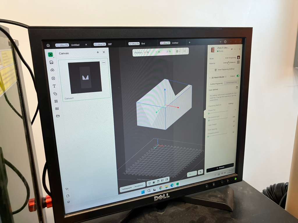
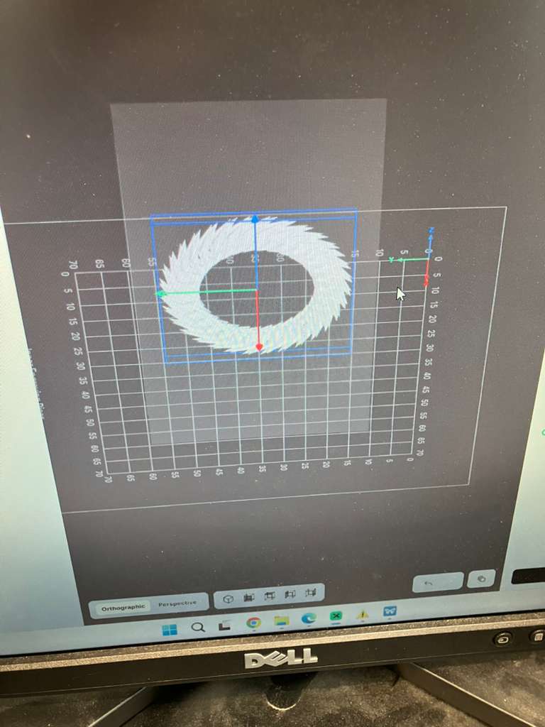
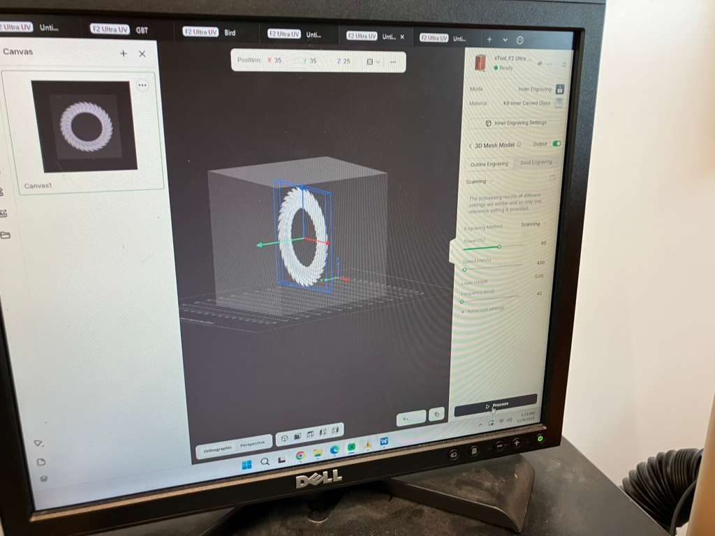
This project explores volumetric glass engraving using UV laser technology, a process not covered in previous assignments. The workflow involves preparing 3D geometry, selecting appropriate lenses for surface or volume engraving, and using scanning mode to create detailed engravings in glass substrates.
Tools and Equipment
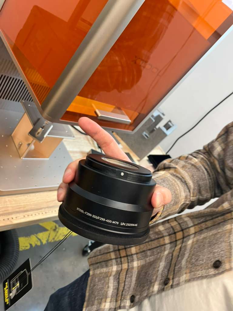
- xTool F2 Ultra UV Laser: UV laser engraver capable of volumetric glass engraving with configurable focal length lenses
- xTool Software: Control software for geometry loading, parameter configuration, and laser operation
Lens Selection
Two types of lenses are available for different engraving applications:
- Long Focal Length: Optimized for surface engraving with lower angle and reduced focus penetration
- Short Focal Length: Optimized for volume engraving with higher angle and increased focus penetration
Workflow
- Start with a test piece to verify settings and focus
- Load the geometry of your glass object (cube, prism, etc.) into the software
- Configure scanning mode with default parameters
- If device not connected, click the connection tab at the top and connect the F2 Ultra
- Begin engraving process
File Formats
The software accepts any 3D file format, including STL files for geometry engraving.
Starting Material
- K9 Glass: Standard glass substrate for UV laser engraving. Available options:
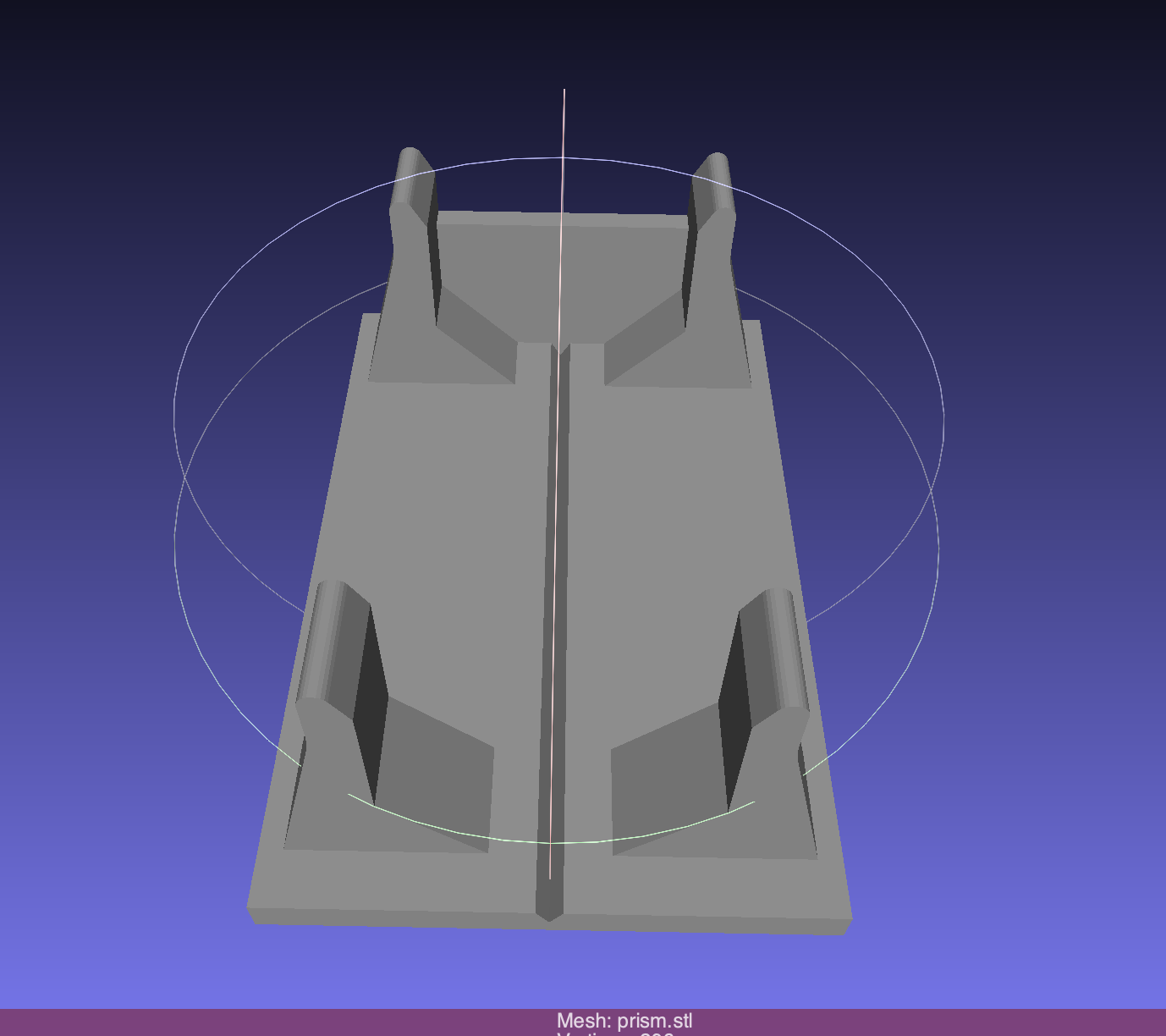
- Flat Surface Requirement: Requires a flat enough face for optimal engraving. Easiest with cubes, or prisms mounted on 3D-printed holders
Design Tools
- PrusaSlicer: Combine multiple STL files into a single design
- Image2STL: Convert images to STL format for image engraving (imagetostl.com)
Engraving Process Documentation
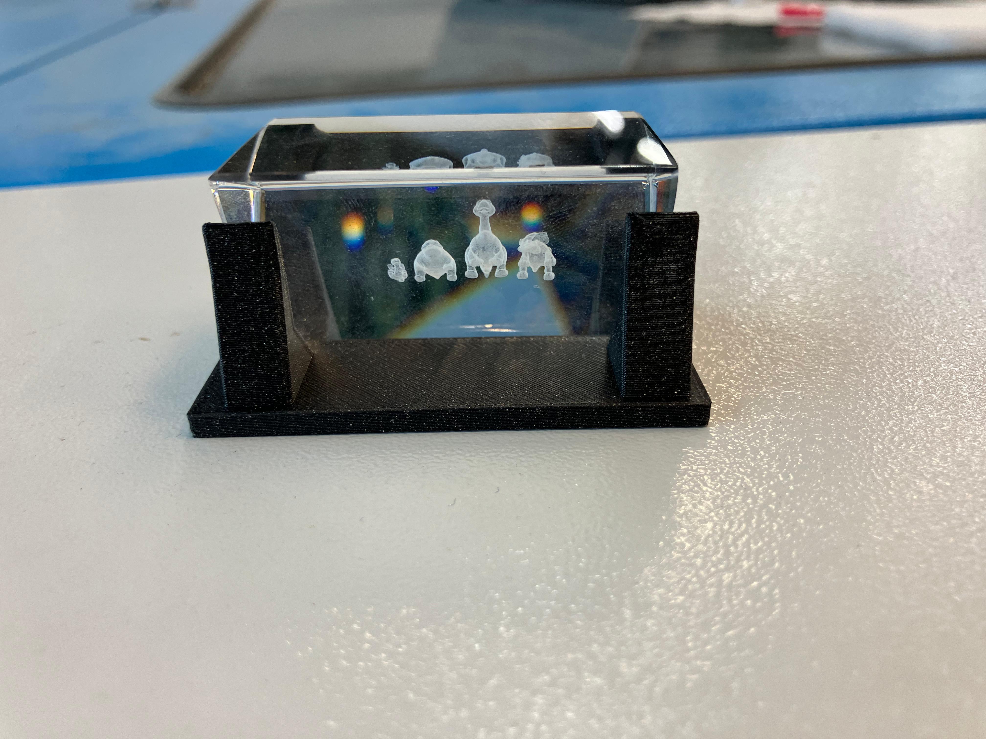
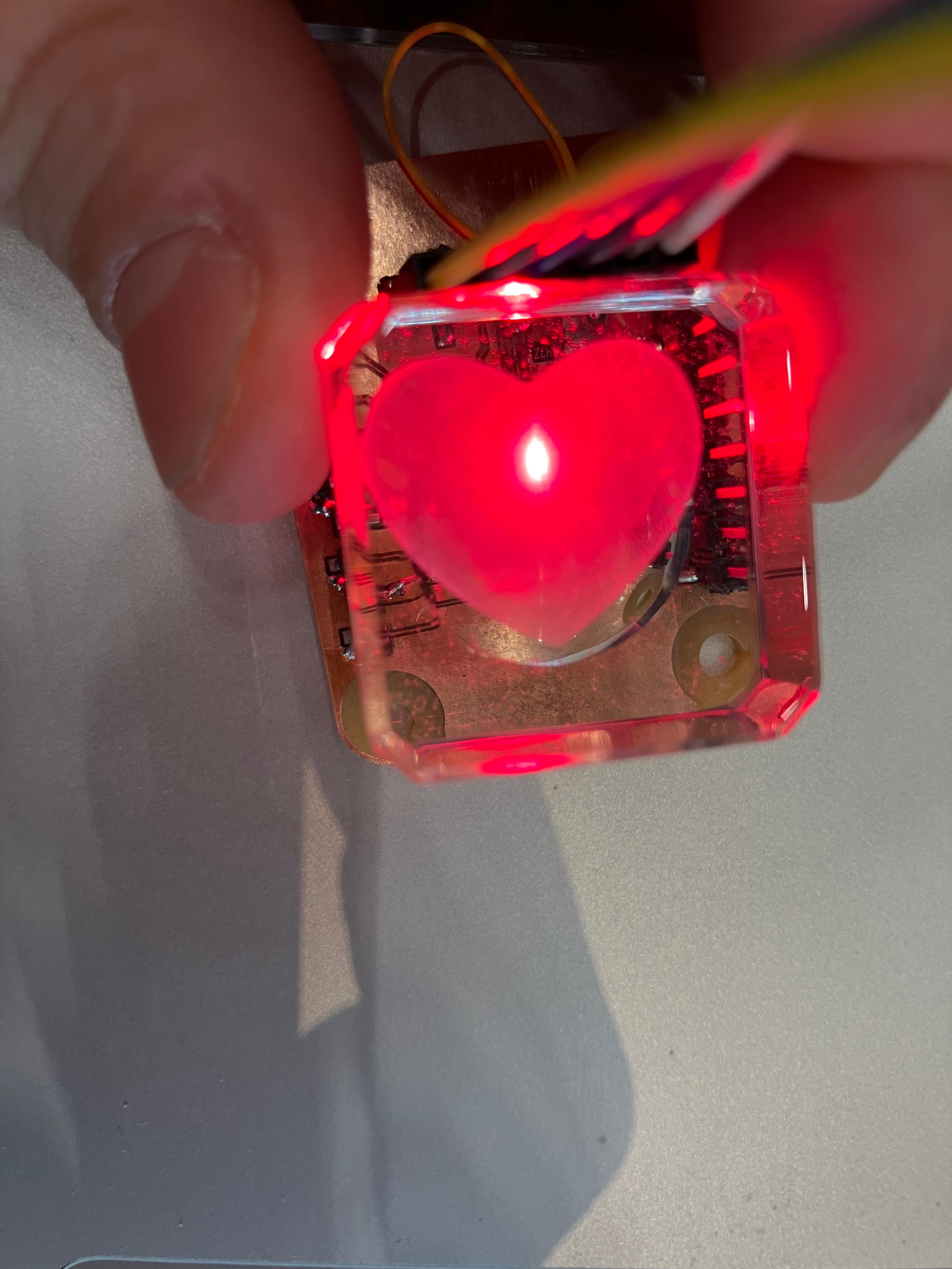

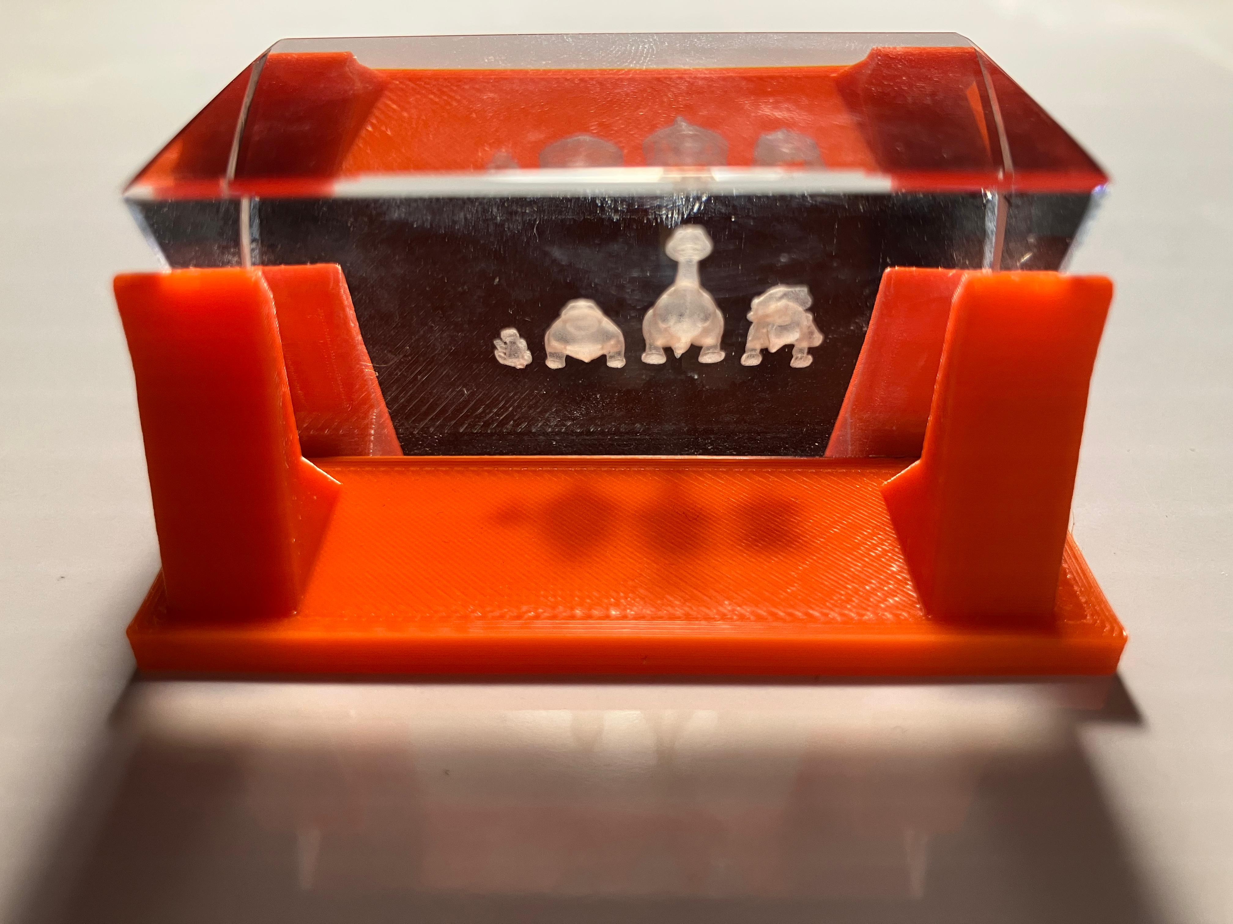
Wildcare Integration: Tiny Blinking Heart
Integration of PCB engraving and glass engraving techniques to create a combined system demonstrating the potential for heart rate visualization through engraved glass from a tiny engraved PCB.
Integration Process
This project combines two wildcard week processes: PCB engraving with fiber laser and glass engraving with UV laser. The engraved PCB contains a blinking LED circuit, while the glass piece features a tiny heart engraving. By centering the engraved heart on top of the blinking engraved PCB, the LED light passes through the volumetric glass engraving, creating a visible blinking effect.
This integration demonstrates the potential for using a back LED to visualize data through glass engravings. For the final project, this technique will be used to demonstrate heart rate readings through a glass engraving from a tiny engraved PCB, creating an elegant visual feedback system that combines digital fabrication processes with embedded electronics.
Wildcard Assignments: Wildcard Week Digital Process
Design and produce something with a digital process (incorporating computer-aided design and manufacturing) not covered in another assignment. This group assignment explores various digital fabrication processes available during wildcard week.
Wildcard Week Possibilities
The wildcard week assignment allows exploration of digital fabrication processes not covered in previous weeks. Possibilities include (but are not limited to):
Machining
- Grinding
- Multi-axis machining
- Electrical discharge machining (EDM)
- Waterjet cutting
- Flatbed cutting
- Plasma cutting
- Laser metal cutting
- Laser micromachining
Welding
Various welding techniques for joining materials.
Molding and Casting
- Vacuum forming
- Rotocasting
Folding
- Mathematics
- Form and function
- Kirigami
Robotics
- Arms
- Construction
- Soft actuation pneumatic inflatable
Electronics
- Pick and place
- Programmable logic
Embedded Programming
- Machine learning
- Machine vision
Food
- Printing
- Gastronomy
Materials
- Synthesis
- Mechanical
- Rheological
Biotechnology
- DIYbio
- iGEM
- HTGAA
- Bio Academy
Textiles
- Fiber processes
- Knitting
- Embroidery (PEmbroider, Ink/Stitch)
- Fabricademy
Composites
Various composite fabrication techniques.
Design Files
Design files for PCB engraving projects including ATtiny1626 and RP2354A development boards.
ATtiny1626 Development Board
Simple development board for ATtiny1626 microcontroller with connectors, resistors, LED, and capacitor. Designed for breadboard compatibility with 100mil spacing grid.
Download Design Files
- ATtiny_QFN.zip — Complete KiCad project files for ATtiny1626 development board
RP2354A Development Board
Complex development board for RP2354A microcontroller with advanced routing and component placement.
Download Design Files
- RP2354A-dev-v1.1.zip — Complete KiCad project files for RP2354A development board
Prism Holder for Glass Engraving
UV laser engraving requires a flat surface for optimal focus and engraving quality. Quentin and Jake designed this 3D-printed holder to securely position prisms during the engraving process, ensuring consistent results on curved glass surfaces.
Download Design Files
- prism.stl — 3D model file for the prism holder
ATtiny1626 Blinking LED Test Code
Simple Arduino-compatible test program for the ATtiny1626 development board. The code configures pin PA1 as an output and toggles the LED on and off with 200ms delays, providing a basic functionality test to verify successful board fabrication and programming.
Code
// ATtiny1626 Blinking LED Test Code
// This simple test program verifies board functionality by blinking an LED

// Define the LED pin using ATtiny1626 port/pin notation
// PIN_A1 refers to Port A, Pin 1 (PA1) on the ATtiny1626 microcontroller
#define PIN_LED PIN_A1

// Setup function runs once when the microcontroller starts or resets
void setup() {
  // Configure the LED pin as an output pin
  // This allows the microcontroller to control the voltage on this pin
  pinMode(PIN_LED, OUTPUT);
}

// Loop function runs continuously after setup() completes
void loop() {
  // Set the LED pin to HIGH (3.3V or 5V depending on board voltage)
  // This turns the LED on by allowing current to flow through it
  digitalWrite(PIN_LED, HIGH);

  // Wait for 200 milliseconds (0.2 seconds)
  // This keeps the LED on for a visible duration
  delay(200);

  // Set the LED pin to LOW (0V)
  // This turns the LED off by stopping current flow
  digitalWrite(PIN_LED, LOW);

  // Wait for another 200 milliseconds
  // This keeps the LED off before turning it on again
  delay(200);

  // The loop() function automatically repeats, creating a continuous blink pattern
  // Total cycle time: 400ms (200ms on + 200ms off)
}
Download Design Files
- ATtiny1626_testcode_blinkingLED.ino — Arduino sketch for blinking LED test on ATtiny1626
ATtiny1626 Library Installation
To program the ATtiny1626 microcontroller in Arduino IDE, you need to install the megaTinyCore board package. This core provides support for the ATtiny series microcontrollers, including the ATtiny1626. Installation instructions are available at the megaTinyCore GitHub repository.
Installation Steps
-
Add Board Manager URL: File → Preferences, enter the following URL in "Additional Boards Manager URLs":
http://drazzy.com/package_drazzy.com_index.json
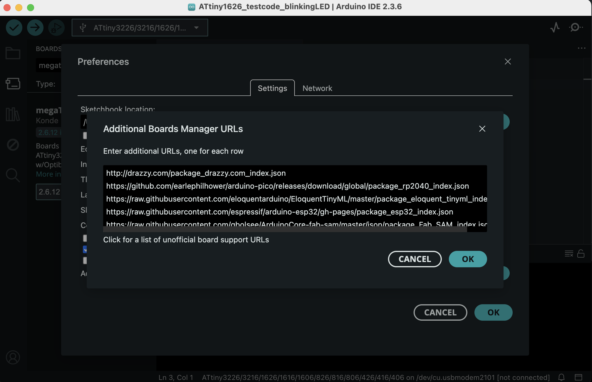
Adding board manager URLEnter the megaTinyCore board manager URL in the Preferences dialog under Additional Boards Manager URLs. -
Open Boards Manager: Tools → Boards → Boards Manager... and search 'megaTinyCore' under the libraries tab. Install "megaTinyCore by Spence Konde".
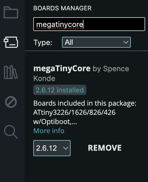
Installing megaTinyCoreSearch for 'megaTinyCore' in the Boards Manager and install the package by Spence Konde. - Wait for installation: Wait while the list loads (takes longer than one would expect, and refreshes several times).
-
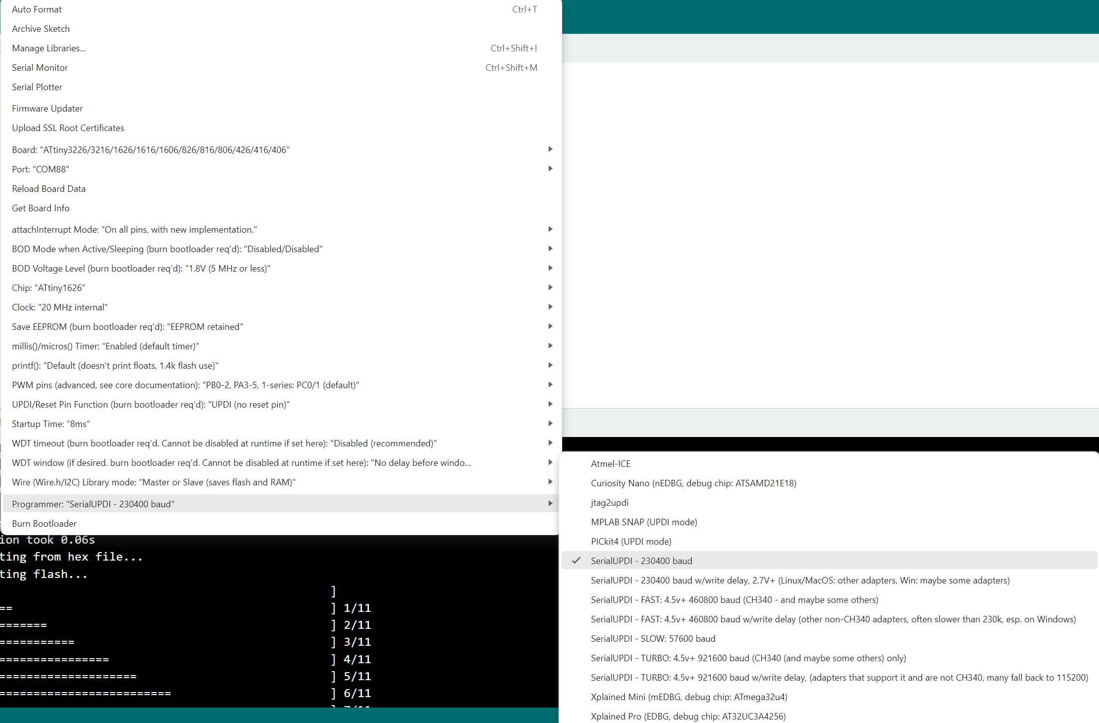
Select board: Select the board 'ATtiny3226/3216/1626/1616/1606/826/816...' option (without OptiBoot) from the Tools → Board menu.
Board selection menuNavigate to Tools → Board to select the ATtiny1626 board. 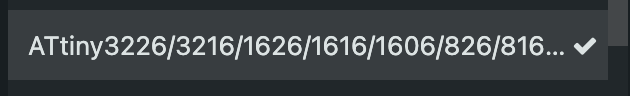
ATtiny1626 selectedSelect 'ATtiny3226/3216/1626/1616/1606/826/816...' (without OptiBoot) from the board list.
Reflections & Learnings
Key insights and learnings from this week's wildcard activities, including glass and PCB engraving.
Key Points
- Advanced fabrication techniques (fiber laser PCB engraving, UV laser glass engraving) require understanding material properties and machine parameters
- Material-specific parameters (power, speed, focus) significantly impact engraving quality and depth
- Achieving desired aesthetic and functional results with new tools demands iterative experimentation
- Integrating diverse fabrication methods enables novel design possibilities and material combinations
- Wildcard weeks provide opportunities to explore advanced techniques beyond core curriculum requirements
Wildcard Week Insights
- Exploring advanced fabrication techniques like fiber laser PCB engraving and UV laser glass engraving.
- Understanding the material properties and machine parameters for novel processes.
- Challenges in achieving desired aesthetic and functional results with new tools.
- Integrating diverse fabrication methods into a cohesive project.
Contributions
Acknowledgements and team roles for wildcard week PCB engraving work.
Wildcard Week Session
- Quentin and Anthony: Ran the wildcard week PCB engraving session, providing guidance and support for PCB engraving projects.
- Quentin: Designed the RP2354A development board before the session and finished the ATtiny1626 design with us during the wildcard session.
- Quentin: Running the glass engraving session and helping us with glass selection andthe design files.
Ethical AI Use
Transparent documentation of AI assistance used in this week's wildcard week assignment page creation.
📋 General Guidelines: See General Commands for Cursor on the homepage for standard guidelines and commands used consistently throughout documentation development.
Week 13 Assignment Page Creation
Complete Cursor AI transcript for Week 13 wildcard week assignment page creation. This comprehensive conversation covers the creation and population of the Week 13 HTML page, including lecture and recitation notes, PCB engraving assignment documentation, design files integration, and comprehensive page structure development. The transcript demonstrates the collaborative process of building professional documentation with structured content, embedded media, and comprehensive design file documentation.
Related to: Complete Week 13 documentation including Lecture Notes, Recitation Notes, Assignment, Group Assignment, Design Files, and overall page structure
Week 13 Glass and PCB Engraving Updates
Complete Cursor AI transcript for Week 13 glass engraving and PCB engraving assignment updates. This conversation covers the addition of glass engraving assignment documentation, updates to PCB engraving process documentation with step-by-step media, design files additions including prism holder and ATtiny1626 test code, highlights reorganization, and image sizing optimizations for better step-by-step documentation flow.
Related to: Glass Engraving Assignment, PCB Engraving Assignment, Design Files, Week Highlights, and Wildcare Integration
 This work is licensed under a
Creative Commons Attribution-NonCommercial-ShareAlike 4.0 International License
This work is licensed under a
Creative Commons Attribution-NonCommercial-ShareAlike 4.0 International License