Electronic
Design
Mastering the art of PCB design. From probing I2C signals on an oscilloscope to designing a custom development board for the Xiao RP2040 using Fusion 360 Electronics.
- Group Assignment: Use the test equipment in your lab to observe the operation of an embedded microcontroller.
- Individual Assignment: Use an EDA tool to design an embedded microcontroller system using parts from the inventory, check its design rules for fabrication, and simulate its operation.
01 · Group Assignment: Oscilloscope Probing
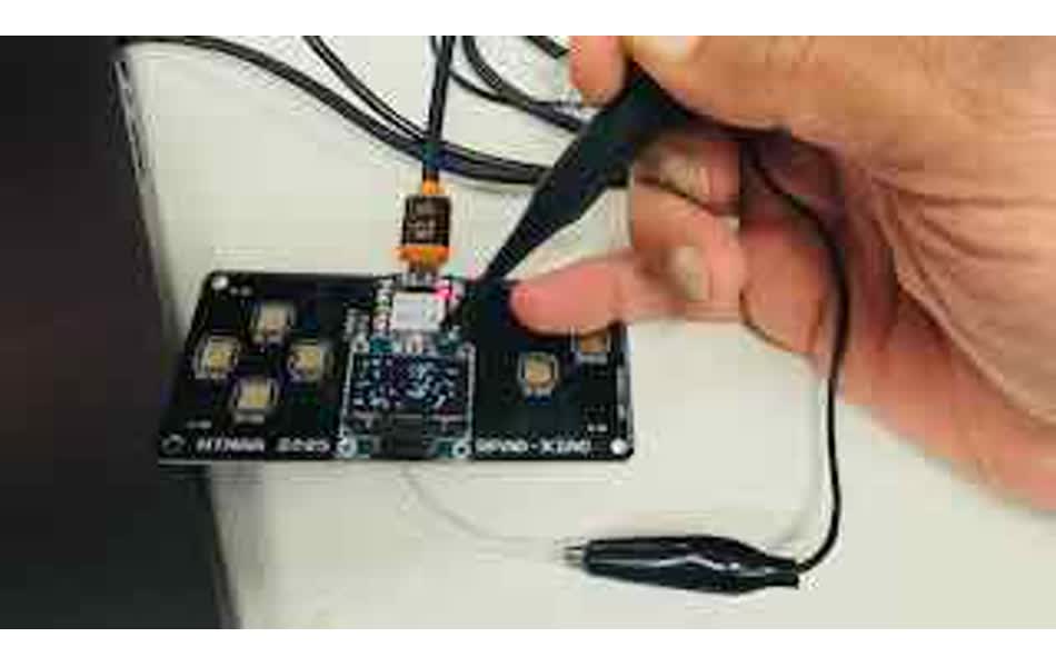
I took my XIAO with RP2040 that we had soldered on the PCB board earlier in Week 03 and hooked it up to my computer running Arduino IDE. I probed the signals coming out of the output pins of the XIAO package, specifically the I2C lines driving the display.
Checking the SCL (Serial Clock Line)
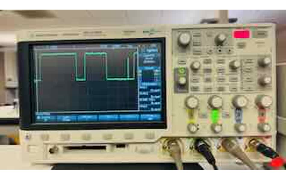
Below is the oscilloscope trace of the SCL from my OLED display's I²C communication while the Game of Life program is running.
- The square wave pattern represents the clock pulses generated by the RP2040.
- Each high–low transition corresponds to one clock cycle, synchronizing data transfers.
- The voltage level is around 3.3V, confirming proper logic levels.
Checking the SDA (Serial Data Line)
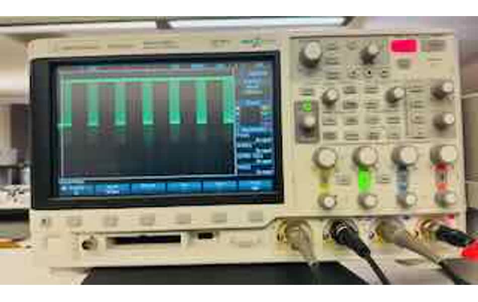
The SDA pin carries the actual data. It's a bidirectional line used for sending commands and receiving data.
- The uneven waveform represents the binary data (1s and 0s) being transmitted.
- Bursts of activity correspond to data frames sending pixel updates.
- Short idle periods indicate the bus is waiting for the next frame.
02 · Individual Assignment: EDA with Fusion 360
I used AutoCAD Fusion Electronics to design an embedded controller system. I decided to align this project with my final project, the SmartPi Agentic Assistant, using the Raspberry Pi Pico RP2040.
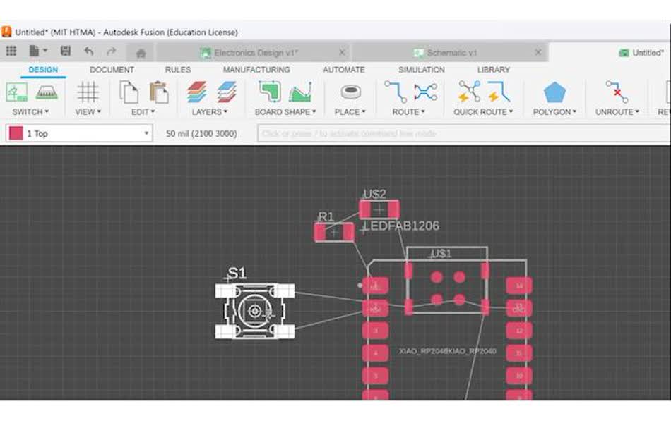
Schematic Capture
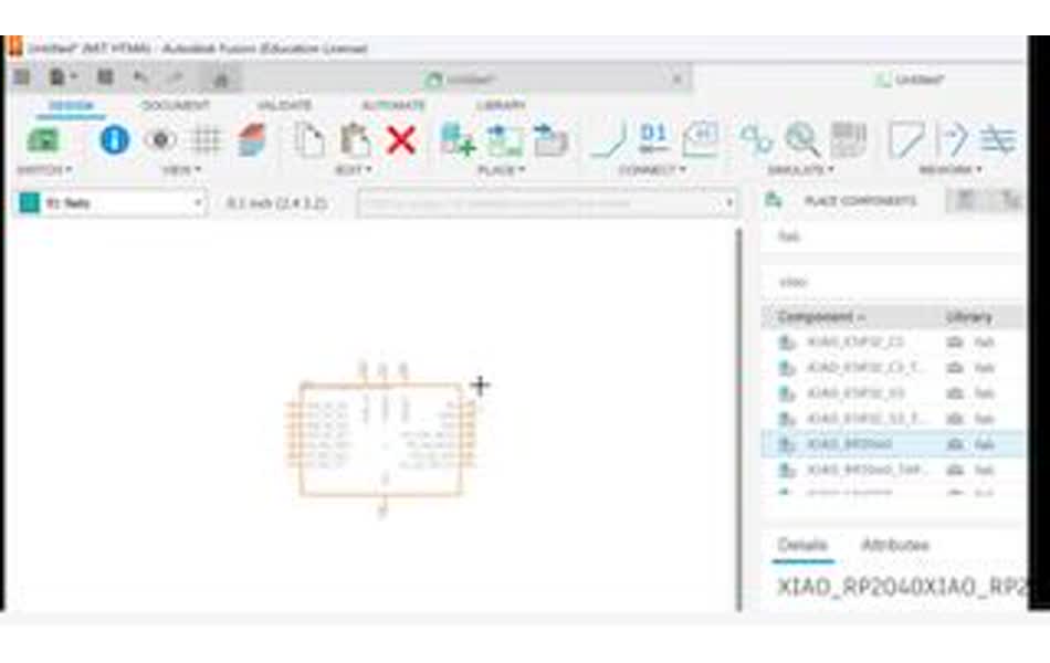
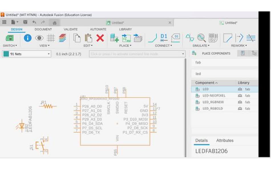
1. Component Selection: Picked the XIAO_RP2040 from the library. Added a switch, a
resistor, and an LED.
2. Connections: Connected the components using Nets. Added labels to keep the
schematic clean.
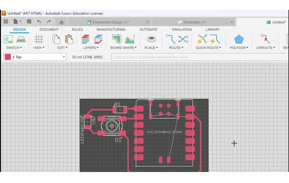
PCB Layout
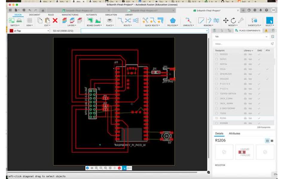
Moved to the PCB editor to arrange components and route traces.
- Placement: Arranged components to minimize trace lengths.
- Design Rules: Updated clearances to 16mil (from default 6mil) for easier milling.
- Routing: Routed traces avoiding 90-degree angles.
- Board Shape: Resized the board, ensuring the USB-C connector sticks out for easy access.
03 · Final Project PCB Design
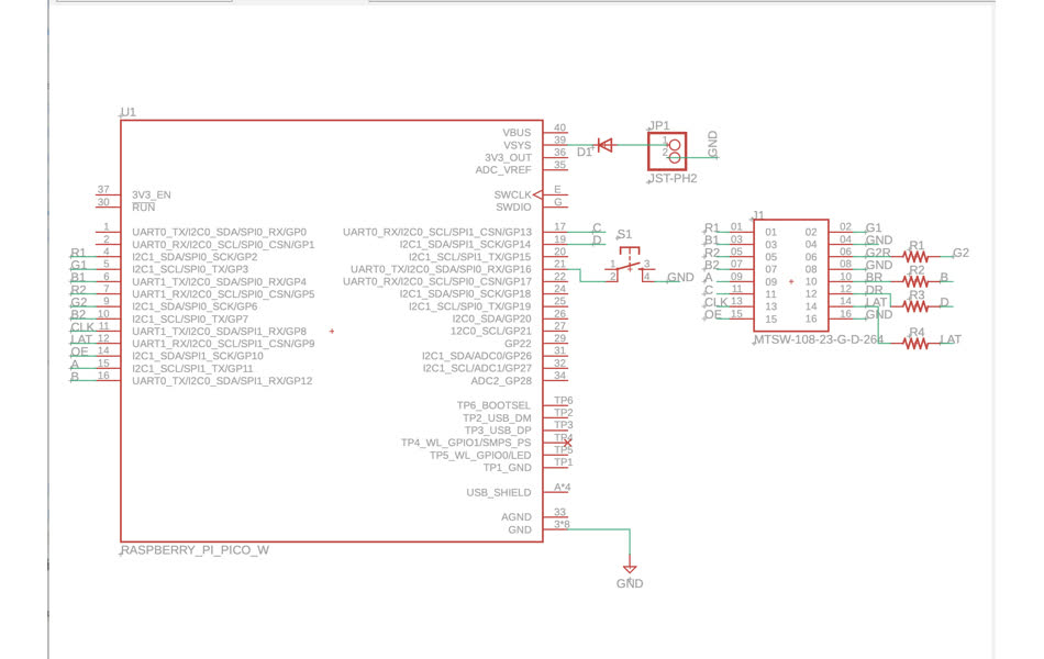
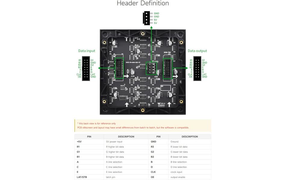
I also designed a PCB for my Final Project, the SmartPi Agentic Assistant. This board acts as a "hat" or carrier board for the Raspberry Pi Pico W, breaking out connections for the HUB75 LED matrix and power.
Carrier Board Design
The design includes a connector for the Pico, a HUB75 connector for the matrix, and power management.
