This week focused on learning how to design, simulate, and fabricate electronic circuits from scratch. We explored the fundamental components—resistors, capacitors, diodes, LEDs, voltage regulators, and microcontrollers—and learned how they come together to form functional circuits. Using tools like KiCad, we designed and routed custom printed circuit boards (PCBs) while understanding schematic capture and design rules. We also learnt about simulating our circuits to verify connections and performance before fabrication. Finally, we became familiar with test equipment such as multimeters, oscilloscopes, and power supplies to troubleshoot and validate our boards, bridging the gap between digital design and real-world electronic behavior.
Group Assignment: Use the test equipment in your lab to observe the operation of an embedded microcontroller
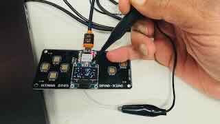
- I took my XIAO with RP2040 that we had soldered on the PCB board earlier in Week 03 Embedded Programming class and hooked it up to my computer running Arduino IDE. Downloaded a sketch (program) into my raspberry pi 2040 and made sure it was working as designed - LED blinking, Hello World on the display screen as well as touch sensors detecting capacitance on the finger, plotted on the Arduino IDE virtual plotter.
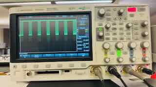
- Now to try and probe the signals coming out of the output pins of the XIAO package, I soldered a small wire to the ground pin of the XIAO (left most pin of the display unit). I clipped the ground wire to the ground clamp of the Oscilloscope and pressed the probe onto the SCL and SDA display pins connected to the XIAO through the pcb.
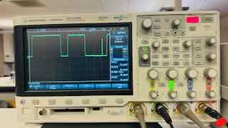
Checking the SCL or Serial Clock Line on the oscilloscope
Below you're looking at the oscilloscope trace of the SCL (Serial Clock Line) from my OLED display's I²C communication while your Game of Life program is running on the XIAO RP2040.
Here's what's happening:
- The square wave pattern you see represents the clock pulses generated by the RP2040's I²C controller.
- Each high–low transition corresponds to one clock cycle, which synchronizes the data transfers on the SDA line.
- The consistent pulse width shows that the microcontroller is regularly updating the display — in this case, sending pixel data for each new frame of your Game of Life animation.
- The voltage level of the signal (typically around 3.3 V for the XIAO RP2040) confirms proper logic levels for I²C communication.
- If you zoomed in on the SDA line at the same time, you'd see data bits changing state while SCL is low — the paired SCL/SDA timing is what defines valid I²C transfers.
In short, the waveform confirms that your RP2040 is actively clocking data to the OLED, with each burst of pulses representing a new screen update as your Game of Life evolves.
Checking the SDA or Serial Data Line on the Oscilloscope
The SDA pin carries the actual data between the master and slave devices. It's a bidirectional line used for both sending commands to and receiving data from the display.
In this oscilloscope image, you're observing the SDA (Serial Data Line) from your OLED's I²C connection while your Game of Life program runs on the XIAO RP2040.
Here's what's happening:
- The uneven waveform—a mix of long and short high and low pulses—represents the binary data (1s and 0s) being transmitted from the microcontroller to the OLED.
- Each data bit on the SDA line is synchronized by the clock pulses on the SCL line (which you saw earlier). When SCL is high, the SDA line remains stable; when SCL is low, SDA can change state to transmit the next bit.
- The bursts of activity you see correspond to data frames, each containing bytes of information such as display commands or pixel updates.
- These data bursts occur repeatedly as your Game of Life simulation updates the display, sending new pixel patterns for each generation of the cellular automaton.
- Between bursts, you may notice short idle periods where the line stays high—this indicates that the I²C bus is momentarily inactive, waiting for the next frame update.
In essence, this trace is a live view of the RP2040 streaming display data to the OLED: every pulse is a packet of bits that redraws part of your evolving Game of Life grid.
Individual Assignment: Use an EDA tool to design an embedded microcontroller system using parts from the inventory, check its design rules for fabrication, and simulate its operation
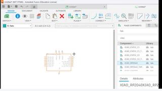
AutoCAD Fusion Setup for doing an Electronic Design
We used the AutoCAD Fusion EDA tool to design an embedded controller system. Anthony took us through the Fusion PCB tutorial
- On Fusion join the MIT HTMA team on the show-data-panel button, top left drop down
- Theres a copy of the fab - part library which we load, have write access on the directory with my name on it for 2025.
- We pick "New Electronics Design" under the file dropdown top left (2nd) and click "New Schematic" under the 'Common' tab.
- Imported the fusion library, open library manager, import lib button, on HTMAA top pick fab library
Creating a New Schematic in Fusion
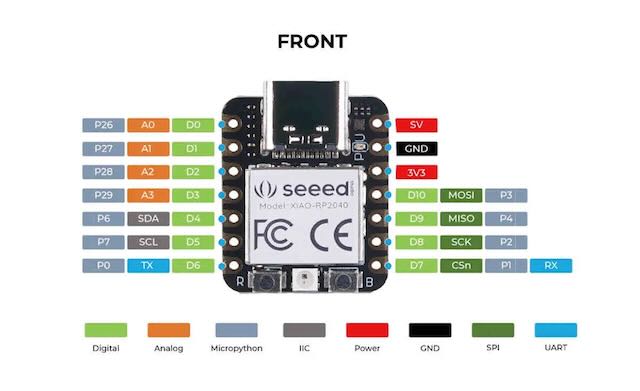
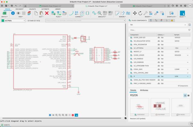
I decided to align my "Electronic Design" week05 project to my final project, esp. Since I'm going to miss about 2weeks in the middle due to an unavoidable India trip. See Final Project link wrt details of my final project. Decided to use the Raspberry Pi Pico RP2040 since it has a lot of pins which meant I could expand my final project without having to design a new PCB from scratch.
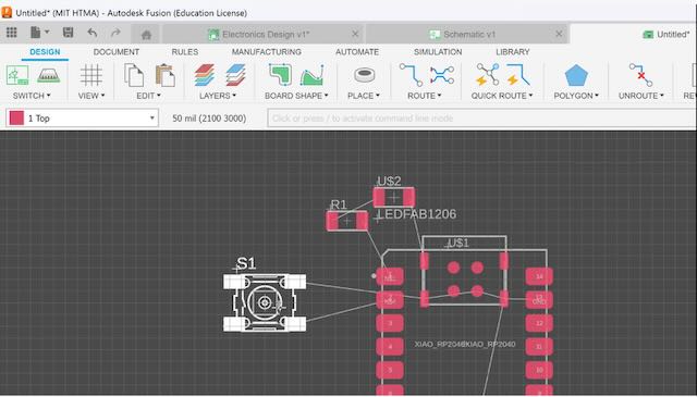
1) We picked the XIAO_RP2040 on the schematic tab. Added a switch a resistor and a LED
2) Connect the components by adding Nets. Add a resistor to A0 (pin1), add a LED to the other end of the resistor, Connect the other end of the LED to the switch, the other end of the switch can go to Pin2 or A1.
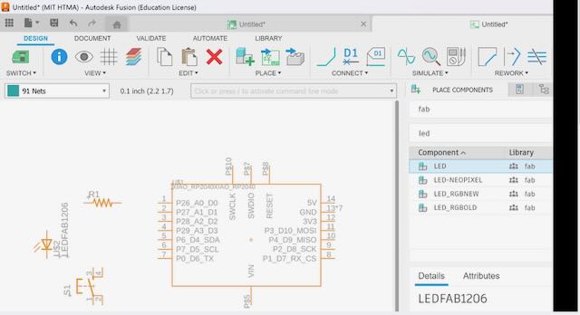
3) Use of labels to keep the net details clean without having to hand draw all the connections. If say 2 nets are named GND, they are considered connected in the schematic view as well as in the layout board. In fact the logical connections is going to show up in the layout view.
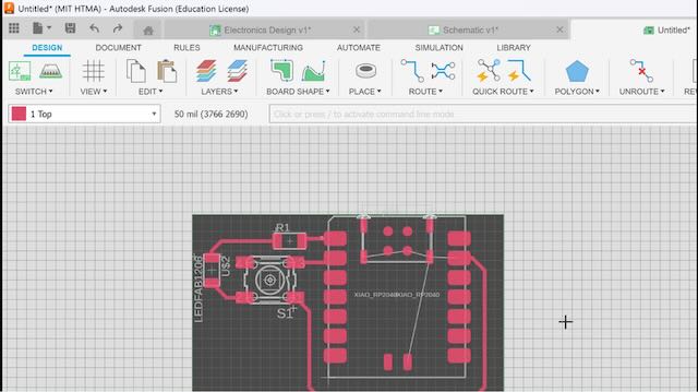
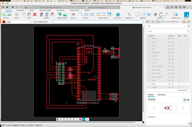
4) Make a PCB for the schematic we've designed. Move all the components to correct positions so the net lengths are short. You can also rotate
- Setup Design Rules.
- Update the Clearances all 16mil from the default 6mil. These are spaces between components and net traces. The layout tool will obey these constraints as we do the layout design with routing traces.
- The holes can also be increased from the 32mil.
- Start routing the traces by connecting the components and pins that need to be connected. The layout tool shows the virtual connection with thin white lines to help route the traces.
- Try not get to edge especially in corners, lay things out in a way that doesnt cause problems later.
- Resize the board to fit the layout. In this case the XIAO USB-C connector should stick out instead of overlap with the PCB board making it hard to connect a USB-C male. So move the USB to the top sticking out of the PCB.
Another PCB board design for my Final Project
I made another PCB design for my Final Project the SmartPi Agentic Assistant, which is a compact, low-power personal assistant built on the Raspberry Pi Pico W, using large language models (LLMs) to convert raw digital data — from your calendar, email, weather feeds, or news sources — into concise text for a 64×64 display, and natural speech via a small speaker.
It bridges the physical world of sensors, displays, and sound with the reasoning power of LLMs, creating a modular platform for context-aware, ambient intelligence at the edge. Think of it as a pocket-sized digital public infrastructure node — open, extensible, and locally controllable.
Here's a system diagram of the hardware device, the software agentic workflow components on the cloud and the Laptop to help get the controller working. WiFi should help simplify the software upload and content management.
Here's a view of the device although it needn't be this bulky. The display and speaker are important output devices. An input mic can be useful for back communication and asking the device to perform actions through voice commands.
Components:
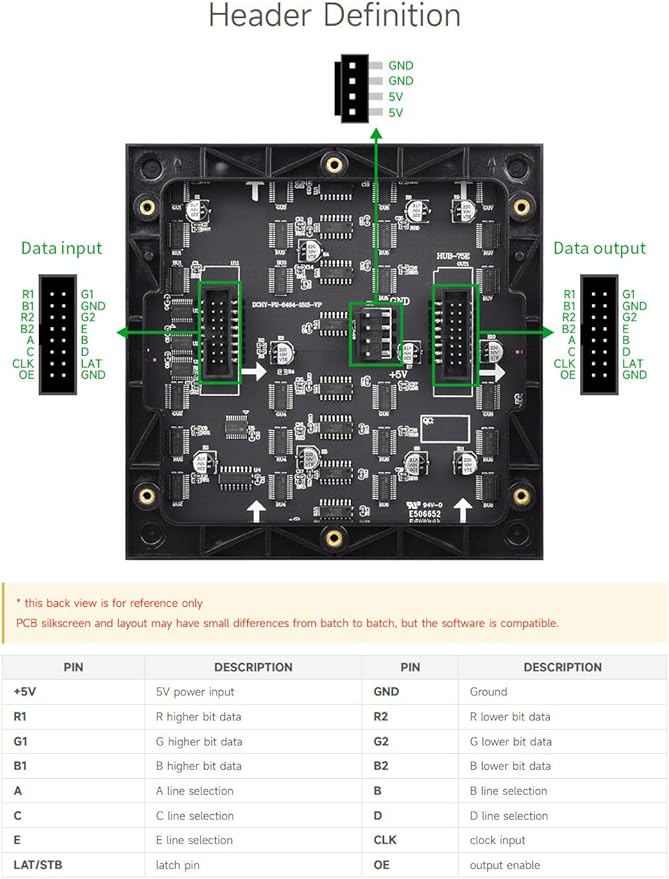
2) PCB Layout for the Pico and PixelMatrix connector which is a HUB75 standard connector.
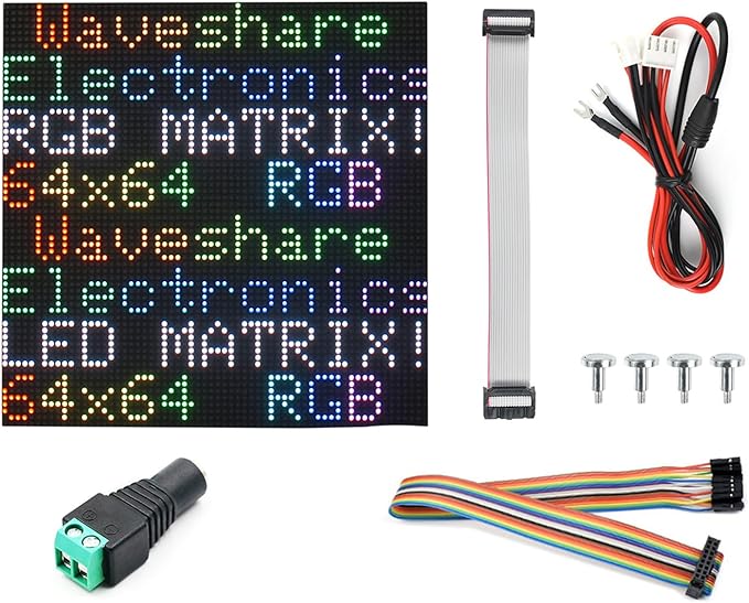
The Pixel Matrix that I need to connect the RP Pico through the connector, the power source and a power switch are included in the PCB design.

The back of the Pixel Matrix board