Electronic Production is where things start to feel real. After weeks of designing and tinkering digitally, we now learn how to actually make our own electronic boards — not order them, but produce them ourselves. The goal is to mill, solder, and program a working PCB from scratch using the fab lab's tools. It's a crash course in precision and patience: setting up the milling machine, carefully soldering tiny surface-mount components, and finally turning a bare copper board into a programmable circuit. This week is about understanding how electronics are physically made — the hidden craftsmanship behind every microcontroller and sensor we take for granted. It's also about developing a feel for the materials and tools, learning how to debug by touch, sight, and instinct. By the end of it, each of us walks away with a working in-circuit programmer — and perhaps more importantly, the confidence that we can make the "brains" of our future projects ourselves.
Group Assignment
1. Characterize the Design Rules for In-House PCB Production Process
The design rules for in-house PCB production are shaped by the precision and limitations of the Othermill (now Bantam Tools) desktop milling machine, which uses 1/64" and 1/32" end mills to cut copper traces and outline boards on FR-1 stock. The 1/64" bit is used for tracing — it defines the minimum spacing and trace width, typically around 0.016" (0.4 mm), which means components and routes must be laid out with careful attention to clearance. The 1/32" bit handles the board outline and larger cuts, providing faster material removal and cleaner edges. To ensure successful milling, traces should not be too fine or too close, pads should have adequate annular rings, and small islands should be avoided. The board's overall design must also consider the toolpath offsets and alignment tolerances of the mill. These rules balance accuracy with manufacturability, producing reliable single-sided PCBs that can be milled, soldered, and debugged entirely within the fab lab — a compact but powerful workflow that turns digital designs into functional hardware within hours.
2. Submit a PCB Design to a Board House
2.1 Hardware Setup and Testing
- I took my XIAO with RP2040 that we had soldered on the PCB board earlier in Week 03 Embedded Programming class and hooked it up to my computer running Arduino IDE. Downloaded a sketch (program) into my raspberry pi 2040 and made sure it was working as designed - LED blinking, Hello World on the display screen as well as touch sensors detecting capacitance on the finger, plotted on the Arduino IDE virtual plotter.
- Now to try and probe the signals coming out of the output pins of the XIAO package, I soldered a small wire to the ground pin of the XIAO (left most pin of the display unit). I clipped the ground wire to the ground clamp of the Oscilloscope and pressed the probe onto the SCL and SDA display pins connected to the XIAO through the pcb.
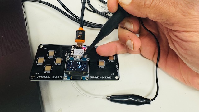
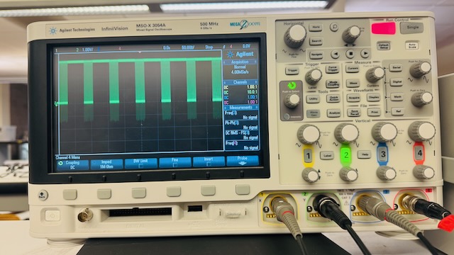
2.2 Oscilloscope Analysis: SCL (Serial Clock Line)
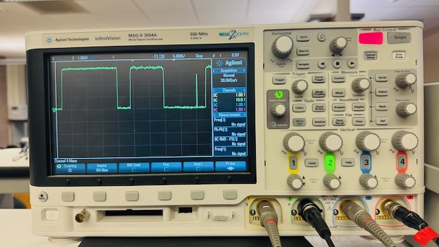
Below you're looking at the oscilloscope trace of the SCL (Serial Clock Line) from my OLED display's I²C communication while your Game of Life program is running on the XIAO RP2040.
Here's what's happening:
- The square wave pattern you see represents the clock pulses generated by the RP2040's I²C controller.
- Each high–low transition corresponds to one clock cycle, which synchronizes the data transfers on the SDA line.
- The consistent pulse width shows that the microcontroller is regularly updating the display — in this case, sending pixel data for each new frame of your Game of Life animation.
- The voltage level of the signal (typically around 3.3 V for the XIAO RP2040) confirms proper logic levels for I²C communication.
- If you zoomed in on the SDA line at the same time, you'd see data bits changing state while SCL is low — the paired SCL/SDA timing is what defines valid I²C transfers.
In short, the waveform confirms that your RP2040 is actively clocking data to the OLED, with each burst of pulses representing a new screen update as your Game of Life evolves.
2.3 Oscilloscope Analysis: SDA (Serial Data Line)
The SDA pin carries the actual data between the master and slave devices. It's a bidirectional line used for both sending commands to and receiving data from the display.
In this oscilloscope image, you're observing the SDA (Serial Data Line) from your OLED's I²C connection while your Game of Life program runs on the XIAO RP2040.
Here's what's happening:
- The uneven waveform—a mix of long and short high and low pulses—represents the binary data (1s and 0s) being transmitted from the microcontroller to the OLED.
- Each data bit on the SDA line is synchronized by the clock pulses on the SCL line (which you saw earlier). When SCL is high, the SDA line remains stable; when SCL is low, SDA can change state to transmit the next bit.
- The bursts of activity you see correspond to data frames, each containing bytes of information such as display commands or pixel updates.
- These data bursts occur repeatedly as your Game of Life simulation updates the display, sending new pixel patterns for each generation of the cellular automaton.
- Between bursts, you may notice short idle periods where the line stays high—this indicates that the I²C bus is momentarily inactive, waiting for the next frame update.
In essence, this trace is a live view of the RP2040 streaming display data to the OLED: every pulse is a packet of bits that redraws part of your evolving Game of Life grid.
Individual Assignment: EDA Tool Design and PCB Production
Use an EDA tool to design an embedded microcontroller system using parts from the inventory, check its design rules for fabrication, and simulate its operation
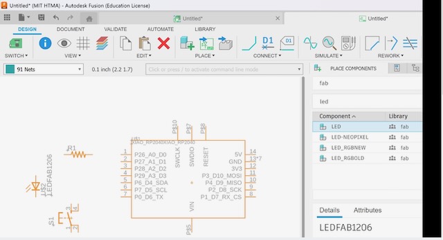
1. AutoCAD Fusion Setup for Electronic Design
We used the AutoCAD Fusion EDA tool to design an embedded controller system. Anthony took us through the Fusion PCB tutorial.
- On Fusion join the MIT HTMA team on the show-data-panel button, top left drop down
- There's a copy of the fab - part library which we load, have write access on the directory with my name on it for 2025.
- We pick "New Electronics Design" under the file dropdown top left (2nd) and click "New Schematic" under the 'Common' tab.
- Imported the fusion library, open library manager, import lib button, on HTMAA top pick fab library
2. Creating a New Schematic in Fusion
2.1 Component Connection and Net Routing
Connect the components by adding Nets. Add a resistor to A0 (pin1), add a LED to the other end of the resistor, Connect the other end of the LED to the switch, the other end of the switch can go to Pin2 or A1.
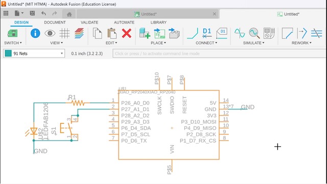
2.2 PCB Layout and Design Rules
Use of labels to keep the net details clean without having to hand draw all the connections. If say 2 nets are named GND, they are considered connected in the schematic view as well as in the layout board. In fact the logical connections is going to show up in the layout view.

Design Rules Configuration
- Update the Clearances all 16mil from the default 6mil. These are spaces between components and net traces. The layout tool will obey these constraints as we do the layout design with routing traces.
- The holes can also be increased from the 32mil.
- Start routing the traces by connecting the components and pins that need to be connected. The layout tool shows the virtual connection with thin white lines to help route the traces.
- Try not get to edge especially in corners, lay things out in a way that doesn't cause problems later.
- Resize the board to fit the layout. In this case the XIAO USB-C connector should stick out instead of overlap with the PCB board making it hard to connect a USB-C male. So move the USB to the top sticking out of the PCB.
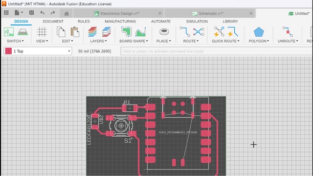
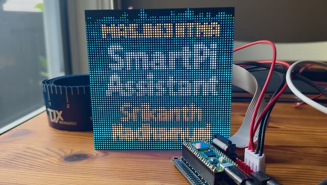
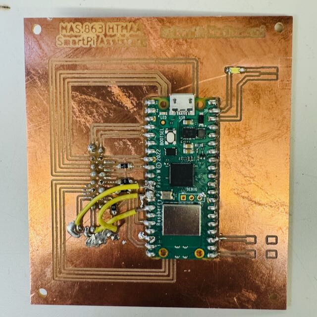
3. Final Project PCB Design: SmartPi Agentic Assistant
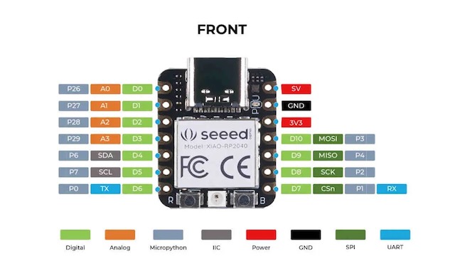
I decided to align my "Electronic Design" week06 project to my final project, especially since I'm going to miss about 2 weeks in the middle due to an unavoidable India trip. See Final Project link for details of my final project. Decided to use the Raspberry Pi Pico W since it has a lot of pins which meant I could expand my final project without having to design a new PCB from scratch.
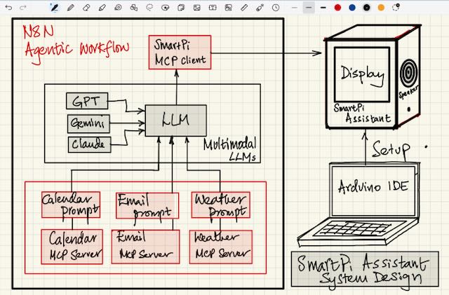
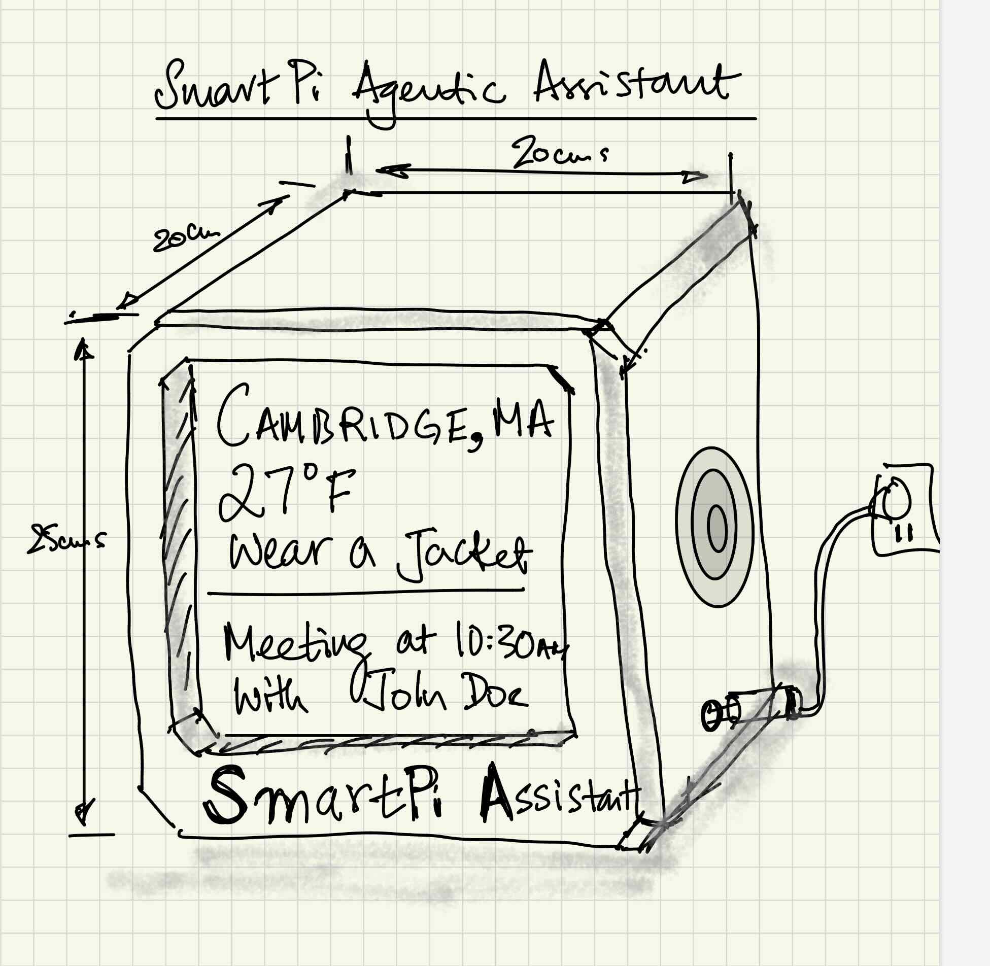
I made another PCB design for my final project the SmartPi Agentic Assistant, which is a compact, low-power personal assistant built on the Raspberry Pi Pico W, using large language models (LLMs) to convert raw digital data — from your calendar, email, weather feeds, or news sources — into concise text for a 64×64 display, and natural speech via a small speaker.
It bridges the physical world of sensors, displays, and sound with the reasoning power of LLMs, creating a modular platform for context-aware, ambient intelligence at the edge. Think of it as a pocket-sized digital public infrastructure node — open, extensible, and locally controllable.
3.1 Hardware Components
Here's a view of the device although it needn't be this bulky. The display and speaker are important output devices. An input mic can be useful for back communication and asking the device to perform actions through voice commands.
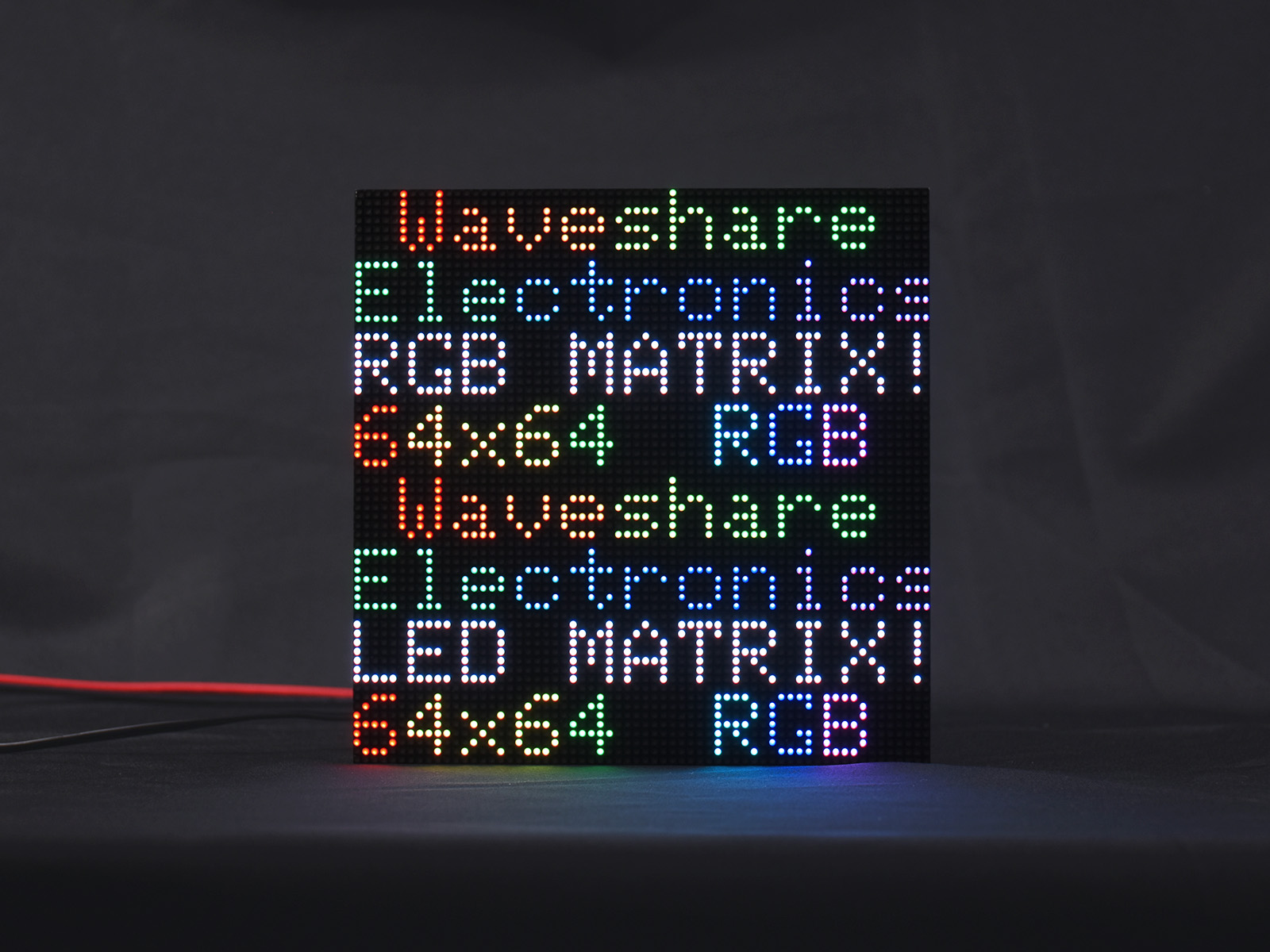
3.2 PCB Design for HUB75 Interface
- I designed a PCB board to interface the above LED matrix panel with Raspberry Pi Pico W with HUB75 standard socket
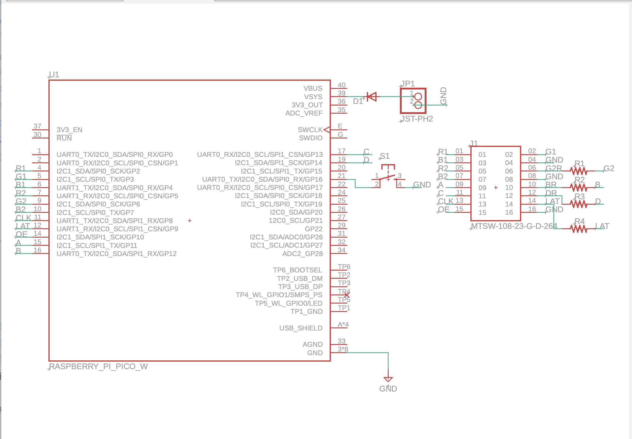
- Created the traces in the layout view with, the power source and a power switch in the PCB design.
There were some crossover issues after the manual trace layout, so dealt with a couple of crossovers using zero ohm resistors as bridges. There were 3 more that I had to deal with. So instead of option for a 2 sided board (and the more involved milling process), I discussed with Anthony and came up with making 3 holes through which we'd run wires and connect the HUB75 CLK, LAT and OE pins from the back of the board, using header pins on the Raspberry Pi Pico.
Added a JST for power and a switch to turn the device on/off.
4. PCB Production Process
4.1 Board Preparation and Milling Setup
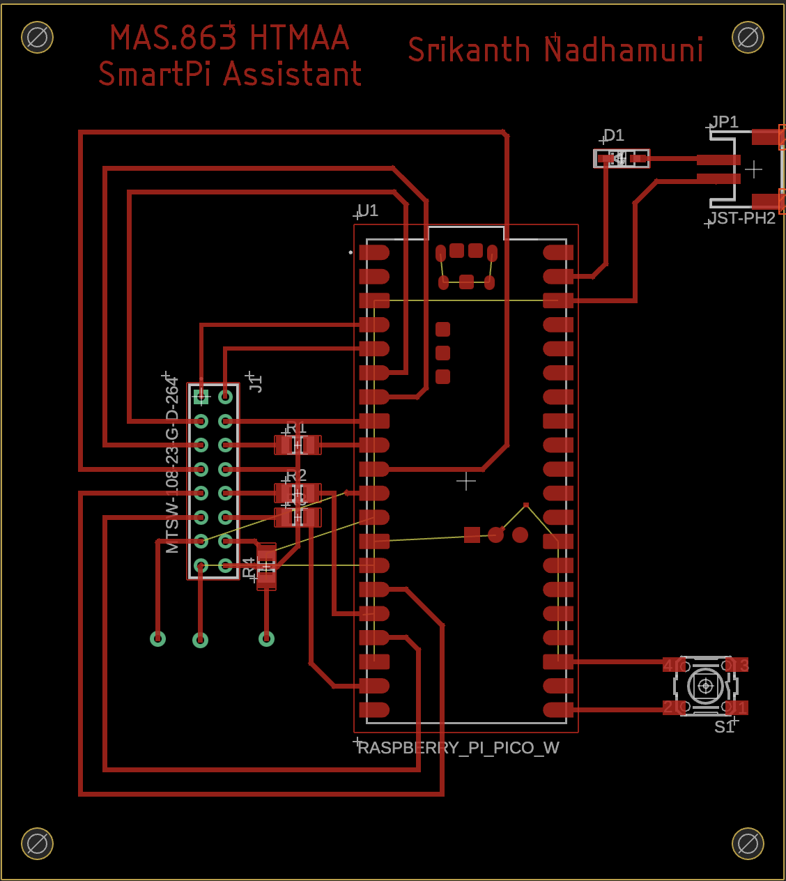
- Created a Eagle 9.x compatible board file with a .brd extension from AutoCAD fusion. Loaded the .brd file on the Bantam software connected to the OtherMill(creative name!!) milling machine.
- Took a single sided board and taped it up using a double sided tape, making sure there are no overlaps (will mess up the milling if the board is uneven)
4.2 Milling Process
- Loaded the 1/64 mill bit and started milling the .brd file
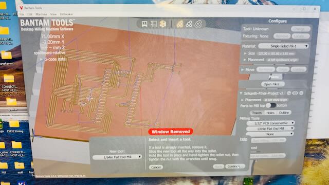
- Clicked "Mill All Visible" with the 1/64" mill bit, to mill the finer portions of the PCB board.
- After the fine milling, loaded the 1/32" larger mill bit, and started the fast milling of the larger board
- After completing all the traces, had to pick the holes and outline to cut using the 1/32" mill bit.
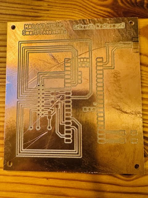
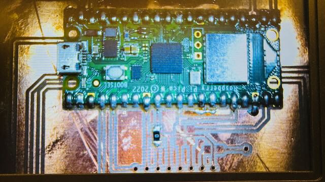
- After all this found that the board was not complete, it was missing the right side of the Raspberry Pi Pico pins and the power points and most importantly the text with course name!!
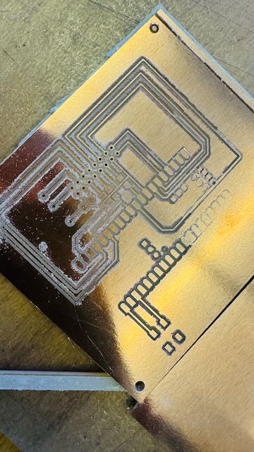
- Anthony, exported a .gerber file and loaded its constituent parts for the trace, holes and outline, and restarted the job, and lo and behold:
- This time the milling machine completed the entire board with all the pins, traces, holes and outline and importantly the text with the course and my name on it, except for the JST power pins, which was no big deal, so we took it for done.
4.3 Component Soldering
- Started soldering the Raspberry Pi Pico W onto the newly printed PCB. The adonstar digital magnifier was super useful in placing the RP Pico W precisely on the correct position on the board, such that the tiny copper pads created by the layout tool was centered correctly.
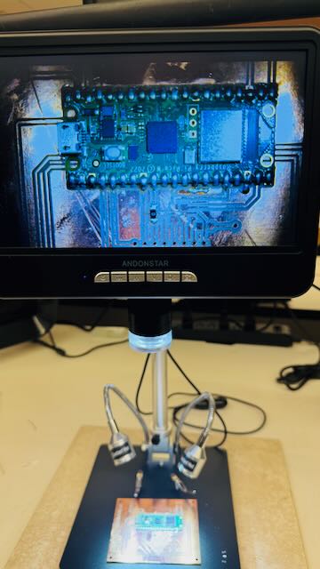
- Cleaned my soldering iron with a small amount of soldering lead to get good flow, then put a blob of solder lead on the bottom left pin and holding the RP Pico W down applied the soldering iron and got one pin securely fastened. After that it was just a matter of getting the rest going.
The digital magnifier was not actually useful to solder, it helped to look directly at the components, but it helped in inspecting the solders and ensure there were no bridges between pins.
- Then proceeded to solder the zero ohm resistors, which were super tiny and difficult to keep in place as the soldering iron and lead came close, it would move and get soldered in weird angles, one needed to heat the trace pad again and ever so slightly move it back into place - this was challenging. But got all 3 zero ohm resistor soldered in place to bridge underlying traces. Test connectivity of the resistors as well as the underlying trace which it was bridging over. All was fine.
- Finally got the diode from the external 5V Vcc point to the VSYS (pin 39) soldered ensuring that the tiny (barely visible) arrow mark was in the correct direction. Added the 3 wires that were needed to avoid the trace crossover challenges.
Project Derisking: Trip to India
I needed to go to India for 10 days for a meeting and event. I knew that the PCB still had the power connections and switch to be connected and the HUB75 pins to be tested. It was unlikely all this was going to work in a day. Then there was the learning about the software environment and then developing the software to test the LED matrix board.
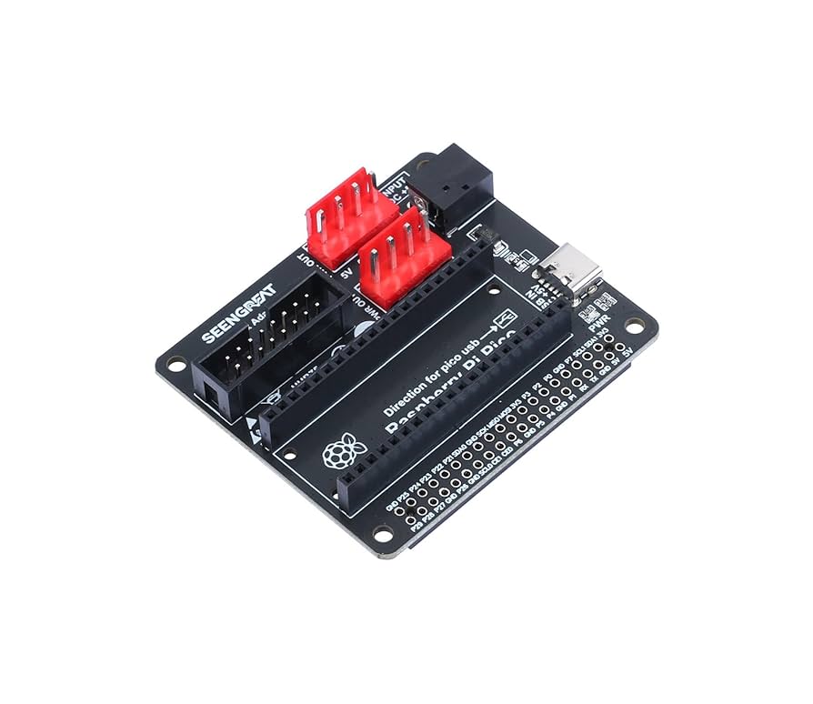
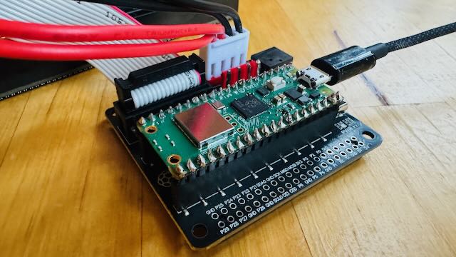
I decided that I would de-risk the project by using a pre-fabricated RGB Matrix Adapter Board, which I had bought when I ordered the Matrix Board itself. Decided to use the adapter to interface the Raspberry Pi Pico W to the RGB Matrix. This was a life saver.
1. Adapter Board Setup
- Installing header pins to the Raspberry Pi Pico so it could be fit into the Adapter board.
2. Connection and Assembly
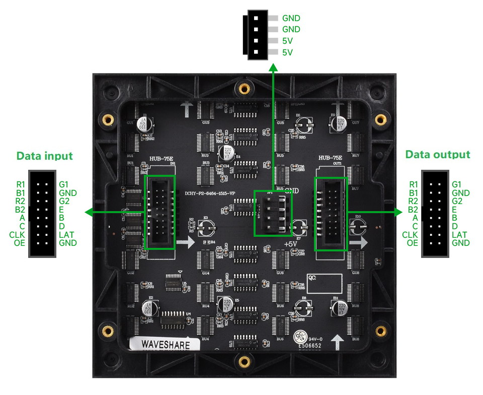
- Pushed the RP Pico W with header pins into the adapter board and connected the a the HUB75 ribbon connector and power supply JST connector. The below diagram shows the 16 pin cable definition and the HUB75 input:
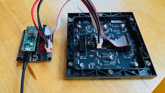
- Connected the adapter card to the RGB Matrix, the below is the connection table
- Connected the micro USB cable into the raspberry Pi Pico and the other end to my Macbook.
The Test program worked!!