

Week 6 documentation
Overview
For this week, the plan is to:- change some stuff from the board designed last week,
- mill the board
- debug it and make sure it works.
Editing the Design
After showing Quentin my design during this week's training I got this feedback:- add connector for external ground/power source
- use 1microfarad nonpolarized capacitors for regulator
- use other xiao board
- connect grounds without vias for single layer
- don't use current control pins to avoid putting RC filters everywhere and use PWM on the on/off control for the electormagnets instead.
To do this, I found the new components (xiao board, capacitors, connectors) in the add window popup and added them to the board.
Then, I changed the wiring according to the feedback and got this:
Now I just have to reroute everything in the pcb.
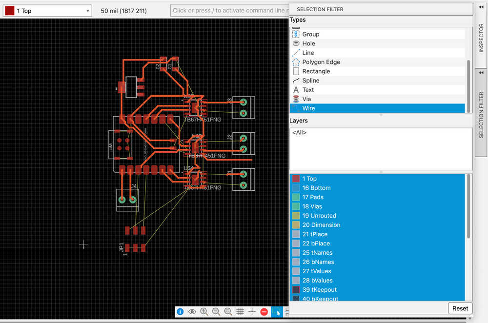
An issue that I immediately encountered was that I wasn't able to move the xiao board into the existing closed board outline. Also I had messed with the selection filter so I couldn't even select the board outline to delete it. Luckily I figured this out and I can now add things to the board.

Now I had to delete the vias somehow. To do this I need to go to the via layer and click on the center of the vias then delete. for some reason this deletes traces instead of the via sometimes.
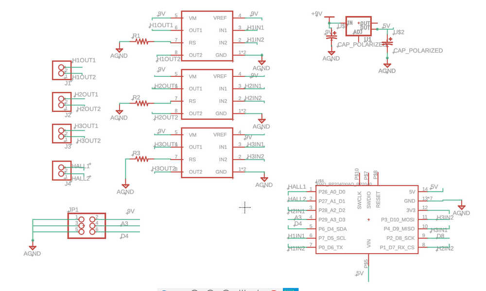
After trying to wire things for a bit, it looks like I should revise my h-bridge placements. Since I only need 2 pins instead of 3 now, maybe there is a better way to do this
I realize I should also remove the ground plate since this will be a single layer now, and after refering to this

I should also remove the resistors for the hbridge current sensing. Heres the new configuration
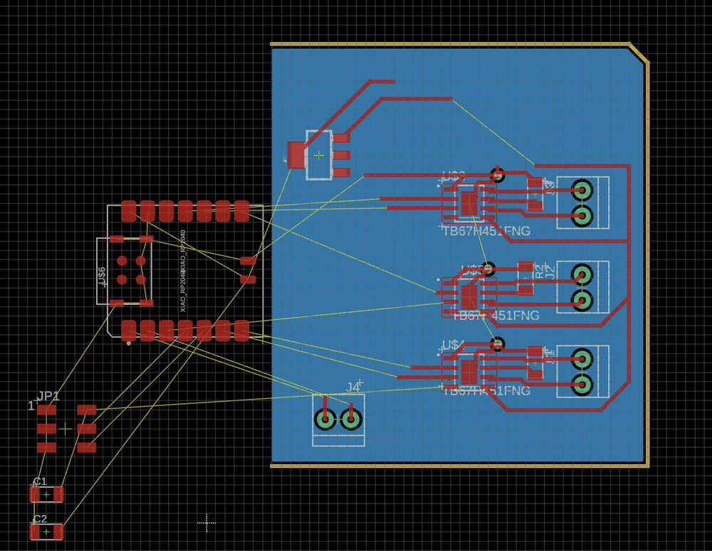
Since I want to start over, I need a way to select all the wires easily. In KiCAD you can hide layers and it looks like you can use selection filters for layers as well as object types. Using the wire selection filter, I select all wires to start over.
After moving back and forth between each document for a while I end up with this:
There is now an added jumper for the 9V and I will need another jumper for the 5V. There are still some things that aren't clear to me, like what inputs of the xiao are actually necessary. But I will figure that out later when things don't work.
Milling the board
Notes from training:Exporting file in Eagle:
edit milling layerrun with gerber file
milling/outline
and fcu, top traces layer
Png from Gerber2img:
white on blackfill edge cut
drag and drop all files into viewer
Png to Gcode:
for gcode export as nc file/gcodemodsproject.org
mods.mit.edu
right click -> programs -> mill 2D pcb
go to left and select img file
set pcb defaults by clicking mill traces
under mill raster
everything should be set up but here are the details:
mill traces 1/64(tool diameter)
.1mm max depth
.1mmcut depth
sort distance checked
offset number: 2
click calculate
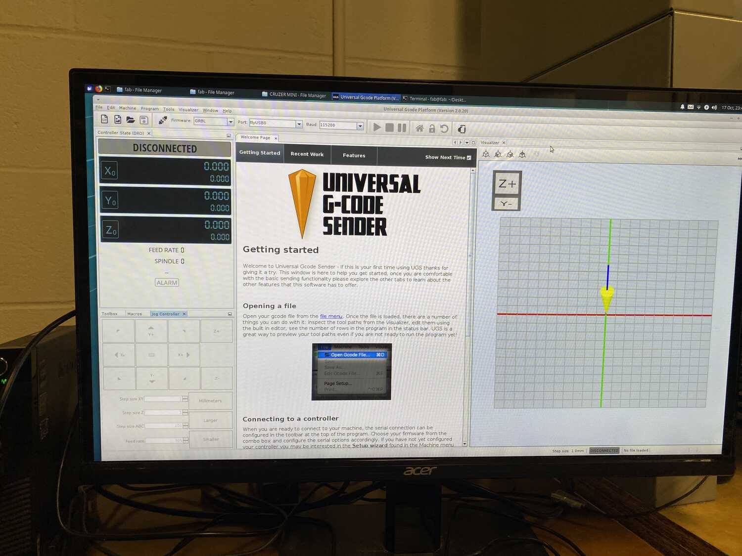
Setting up the router:
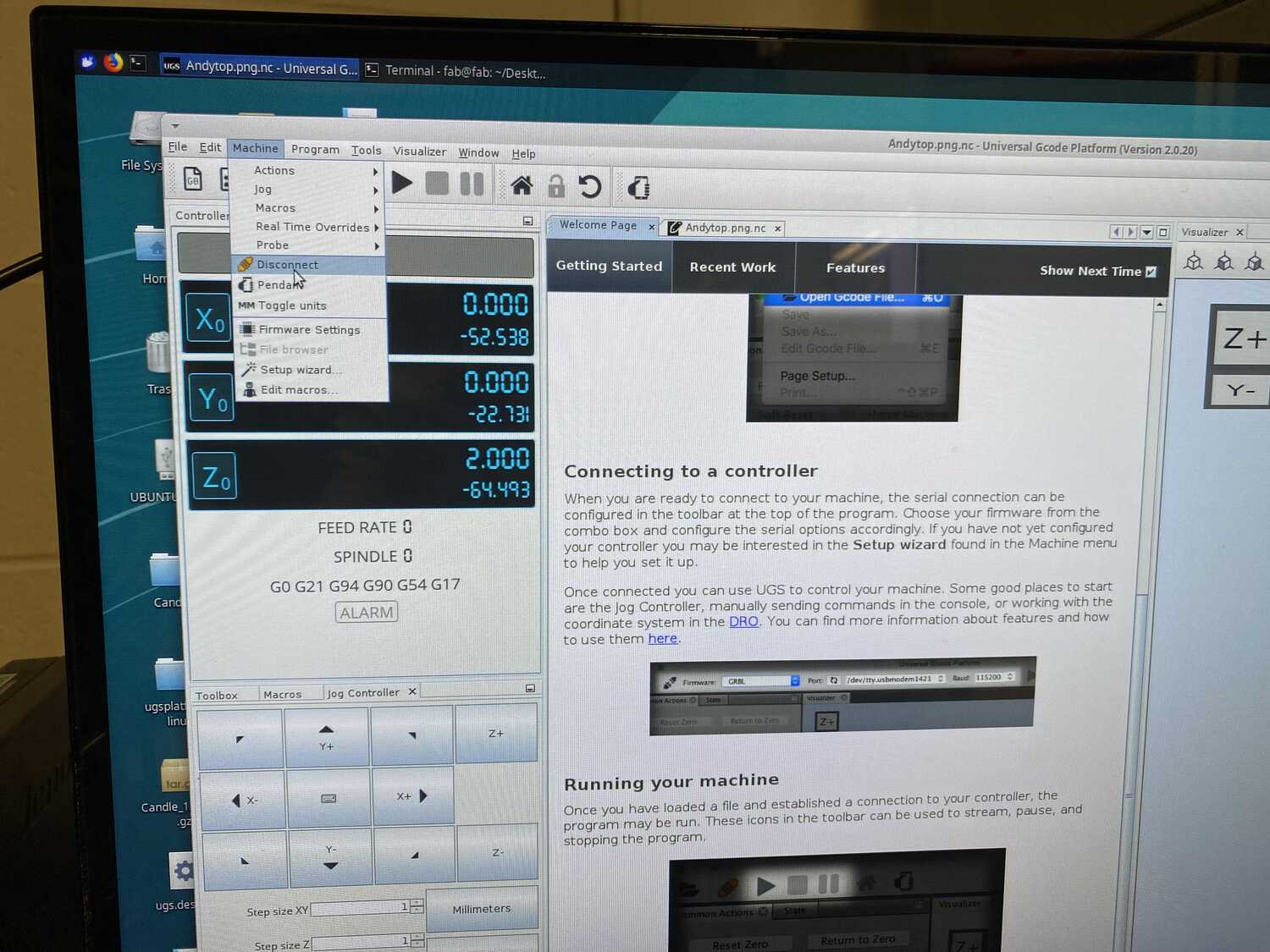
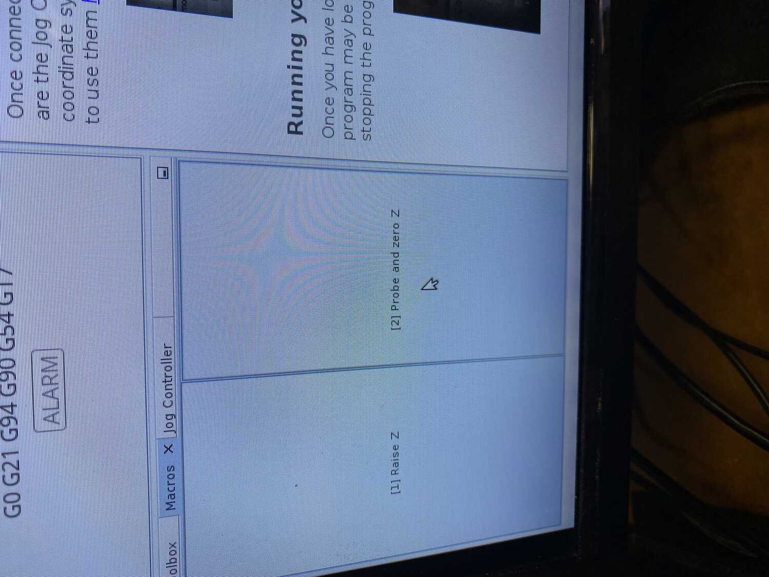
Open the software using the command .\ugsplatform in terminal from /home/fab/Desktop/ugsplatform-linux/bin/Connect to the machine by going to machine->connect
Jog to the bottom left of stock using the controls on the left then click zero x and y
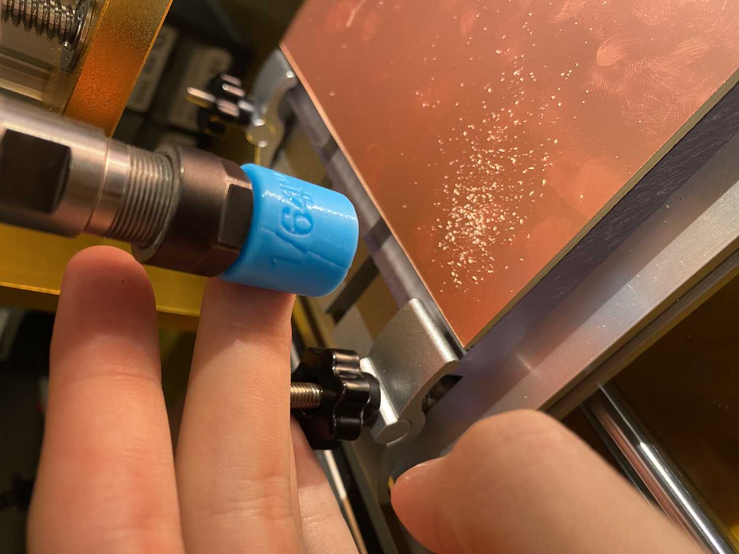
Make sure 1/64th is set up, if not put remove duster and put endmill in the 3D printed holder and tighten clamp using two wrenchs
Put red contact on top rod for zeroing
Put back duster and run macro zero z
in universal gcode platform turn on vaccum and use earmuffs
for cutting outline:
go back to mods, use 1/32 tool diameterclick mill outline sets defaults
.6 cut depth
1.8 max depth
Uses tabs
Change endmill to 1/32
Cut the tabs with something, screwdriver, wear safety glasses lol
OTHER NOTES:
For Outsourcing:
JLC pcb/pcbway
insert 4 files generated when exporting as gerber
1.6 thickness
other black pcb colors are more expensive
surface finish: leadfree HASL silver, (ENIG is gold, doesnt oxidize)
multimeter testing:
sound mode, tests for continuity
to mill out all the copper from the board, use 32 with inf offset and use 0 offset which is infinity
Exporting:
Well this has been a journey.
Here is what I learned:
To export as gerber file, you need to go to the manufacturing tab and click a button that says export gerber.
Now, for the Eagle ulps that export a png file, you need to download the ulps from gitlab here https://gitlab.cba.mit.edu/classes/863.23/site/-/tree/main/doc/EDA_recitation
Then move those to the ulp folder inside of the Fusion 360 folder in your documents
Change the path to the ulps in fusion's preferences by clicking the icon with your initials in the top right and setting it to the place you put the ulps
To run the ulp type "run singleImages"
The ulp's do a bunch of croping, name hiding etc that are a pain to do in photoshop so it is worth it.
Since there have been a few issues with the milling, with the blanks warping under the clamps, zeroing process breaking endmills etc. I decided to find the components first.
Here is the updated component list for the pcb board:
- 3 h-bridges
- 1-2 hall effect sensors
- 5v regulator
- xiao rp2040
- 2 1microfarad capacitors
- 4 1x2 screw terminal blocks
- 1 3x2 headers smd
- 2 jumpers
Since the TB67H451FNG were not in stock at the cba lab, I found some TA's to help during office hours and restock.
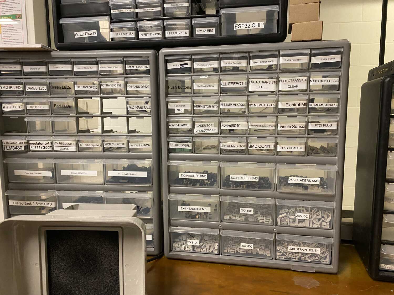
What I have now:

Machining:
Setting up the machine took some work. Following the steps that I outlined above:
After connecting to the machine:
Placing the endmill in the clamp
Jogging to the bottom left corner
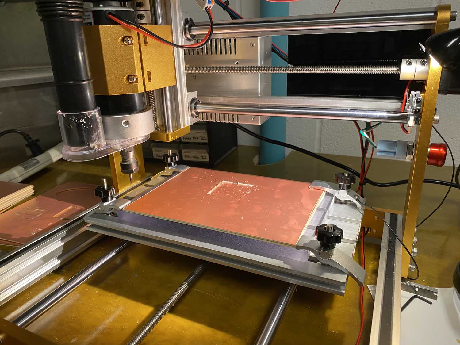
Running the z zero macro
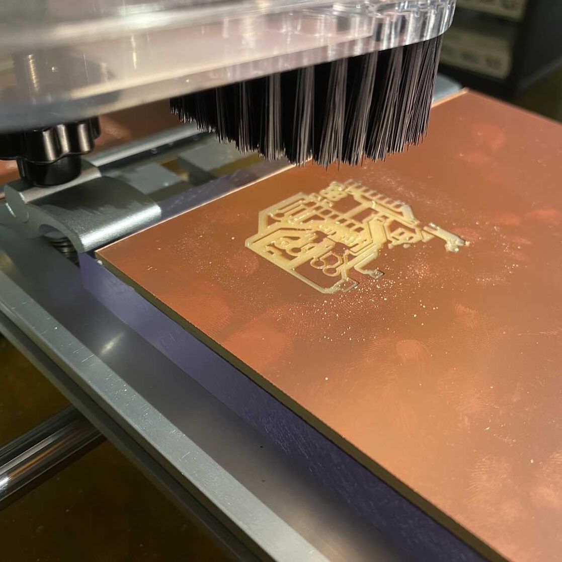
After after hitting run (and turning on the vaccum):
My traces are too thin!
Since its now 1AM I will be giving up for today
Things left to do:
make traces thicker and figure out why drc didnt do anything
mill another board
solder components
test running some stuff for next iteration.
(I do all of these things in input and output week and later)