

Week 9 documentation
Overview
For this week, the plan is to:- catch up from the week 6 assignment to mill and test a pcb
- test out hall effect sensors
what do
After seeing a youtube video about someone building a magnetic rail launcher using electromagnets and hall effect sensors, It seems that hall effect can be useful here which validates my plan.The idea for a sensor is to have some feedback to tune the controls.
(some very sketch-y sketches)

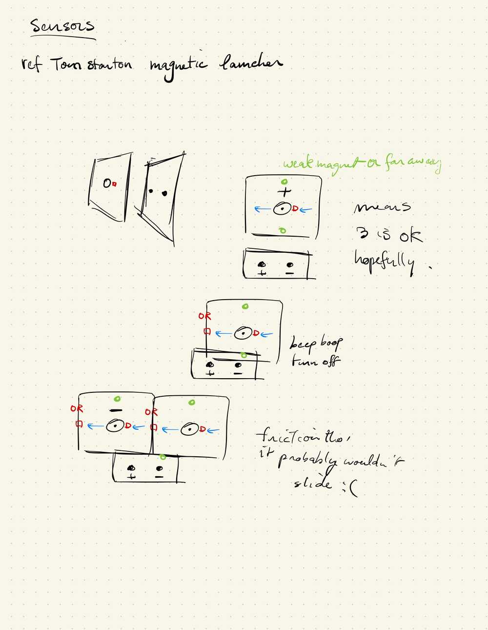
Talking to David, it looks like working with an open loop system would be easier so I shouldn't have to worry about controls and feedback too much although I still don't really understand the implications.
fixing the drc

I fixed the pad clearance and the line widths
David advice:
- the contact traces for chips are spaced really close, make sure there its not occupied by routes
- watch out for routes that are close to corners
milling the board
I repeat the steps from week 6 to do this.

toolpath:

I actually fail about 5-6 times before getting something that doesn't really work. Here is what happened
First mistake
Using the wrong end of the clampsI had notice that while I couldn't tighten the clmaps any more, it did not seem particularly well held together
I ignored it and the board drifted with the vibrations of the machine while it milled

Second mistake
This time everything seemed ok until I looked at parts of the board that were supposed to be done milling: i could still see copper and some other spots had been milled deeper, looking at the board, I noticed it was arching. SInce I couldnt sport the roller anywhere I had just pressed down the board with my hands to make sure the double sided tape was sticking, but that obviously wasnt enough. Maybe the drifting in the first run lifted up the board in the center.
Third mistake
When zeroing for the third time, this time the bit did not stop at the board and smashed through. An alarm went off and I could not jog the machine anymore.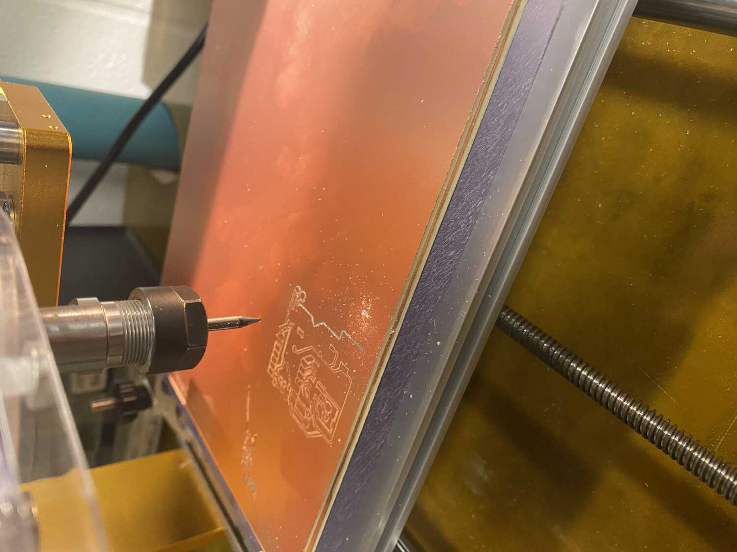

Fourth mistake
The fourth time I zeroed the z It worked fine but I forgot to zero the x and y after I had moved to my start location. Fortunately the machine moved out of bounds and was interrupted before anything bad happened, i reset it by clicking home machine againFifth mistake
After zeroing the machine one more time at the same location, the bit zeroed the first time after the probe was detected, but something happened on the second probing and the bit kept going further into the board and z was in the negativeMy mistake was accidentally clicking jog +y instead of +z which broke the bit
After replacing the bit and successfully zeroing xy and z things seem to be working. Although it seems to be milling a bit deep, i dont really care at this point
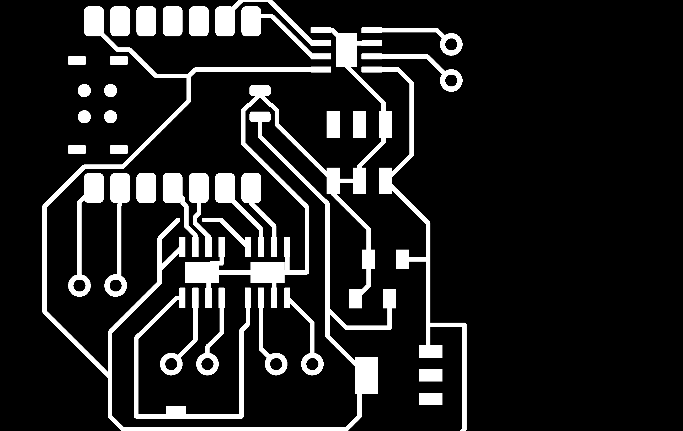
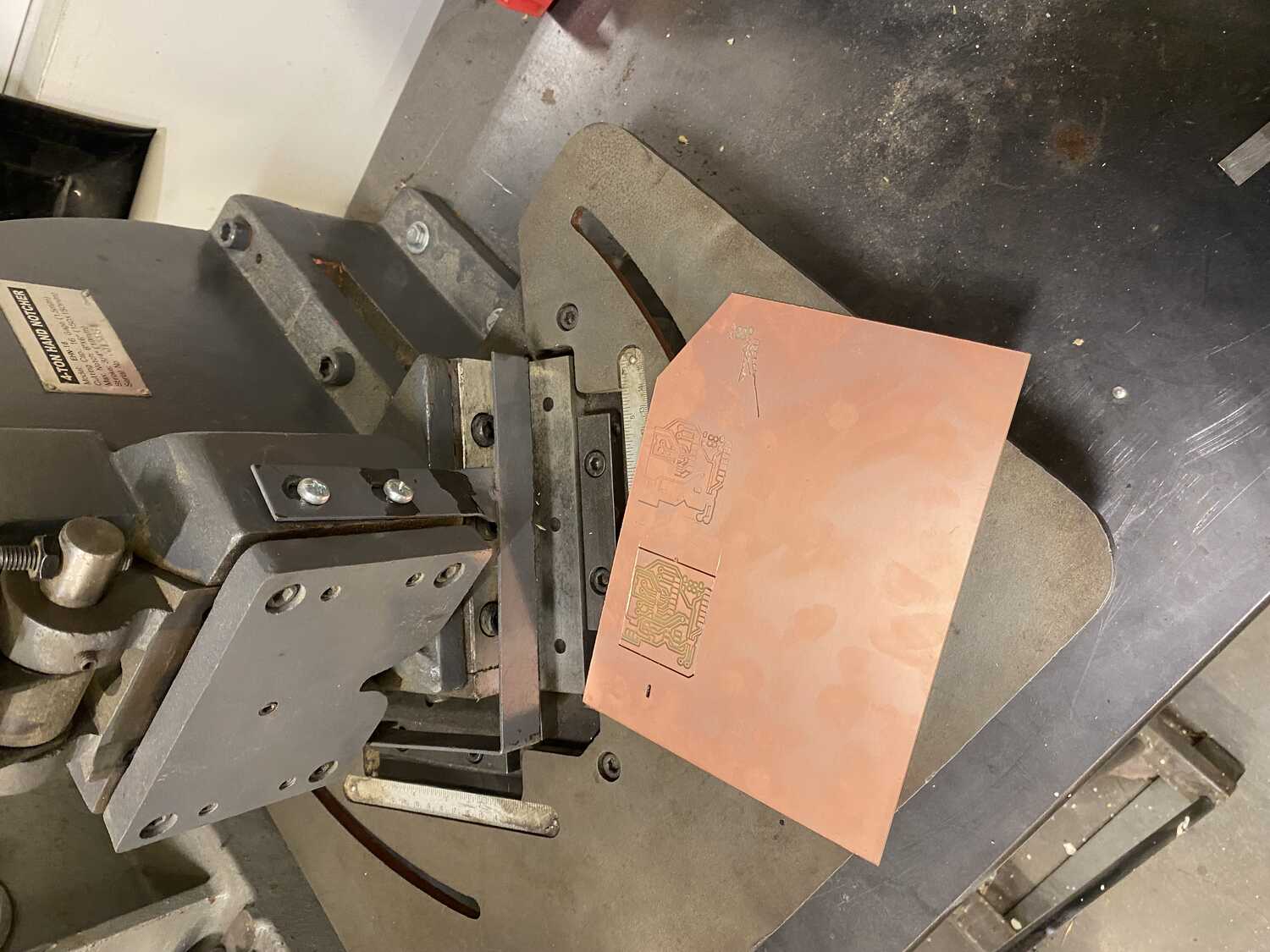
Heres the final board:

Now as you can see, the board was not milled completely! that's because the pngs that were exported from fusion were not cropped properly, as a result, the error propogated into the final job. I noticed this, but just preteneded everything was fine and that I could fix it later.
Fixing it later:
Heres how I got it out of the board. I first scored it with a box cutter, and then used this stomper thing to nibbled off the side of the chip near the edge of the board, then snapped off the other side.
To try to fix the png error, I tried using Quentin's https://quentinbolsee.pages.cba.mit.edu/gerber2img/ Gerber to image converter.
Following the instructions from week 6, I exported the fusion file as gerber under the manufacturing tab, then I found the files and dragged over the file named something like "top copper" for the traces. I checked black and white, fill edge cut, and locked both dimension and origin.
this fixed the traces, but when converting the board, the holes for the connectors were not transfered well.
Soldering
Since I didnt have time during week 6, I'll talk through soldering here. Is what I was planning to do. I'm gonna dive into soldering next weekso that I have time to look at the sensors. Heres the theoretical layout however:
I grabbed a hall effect sensor, but I'm still missing the jumpers, voltage regulator, and the two capacitors.
I did talk to Quentin a bit about the process:
- put a tiny bit of solder on the tip
- heat up traces with tip
- once hot enough, add solder to the copper traces, it should melt.
- remove nib, add component leg.
- heat up both the leg and the trace and remelt the solder on the copper
- once the component is attached, now heat the other parts (both leg and copper) and add solder
programming
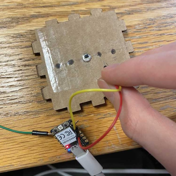
Since I didn't solder anything, I will just test things with jumper wires and a breadboard for now all I want to do is see if I can read anything from the xiao's digital pin using the hall effect sensor.Heres the idea for the code:
#define as analog input, D1
#in loop
#Serial.print.ln(analogread(D1))
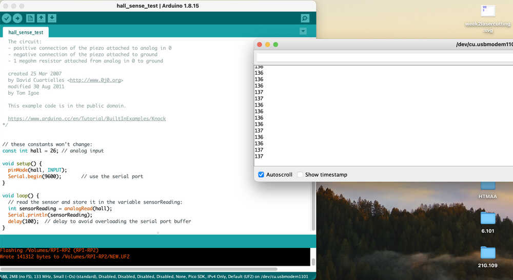
And after modifying some example sensor code:
// these constants won't change:
const int hall = 26; // analog input
void setup() {
pinMode(hall, INPUT);
Serial.begin(9600); // use the serial port
}
void loop() {
// read the sensor and store it in the variable sensorReading:
int sensorReading = analogRead(hall);
Serial.println(sensorReading);
delay(100); // delay to avoid overloading the serial port buffer
}
Once I fixed some bugs uploaded the code, and opened the serial monitor, I realized that it was already printing values! Even though I hadn't connected anything to the board yet.
Just by touching the pin I could get the values to change, acting like a touch sensor!
Well anyway, back to the point.
I need to wire the 3.3v and ground to the hall effect sensor (A1324LLHLT-T) and connect the output pin to the analog input of the rp2040.
I just need to make sure which pin is which by checking the datasheet.

Turns out holding 3 things with 2 hands is difficult.
Nevertheless, here is the setup I went with. It looks like 26 actually referes to the pin labled as "p1" but its reading the input as an analg value anyway.
Also interesting that the read value is lower with higher current and higher with lower current/higher resistance.
The input value changes the closer the sensor is to the magnet, success!
Note on whats left for sensors:
- making the board with connector for the hall effect sensor
- soldering (look at next week)