Welcome to Hellish Cambridge PCB (Part 2)
made with electronics production
To Do
Group Assignment
- characterize the design rules for your in-house PCB production process
- send a PCB out to a board house
Individual Assignment
- make and test the development board that you designed to interact and communicate with an embedded microcontroller
- extra credit: make it with another process
Tools
- Software: mods, Kicad
- Machines: Electronics mill in CBA shop
Materials
- copper clad
- electronics parts
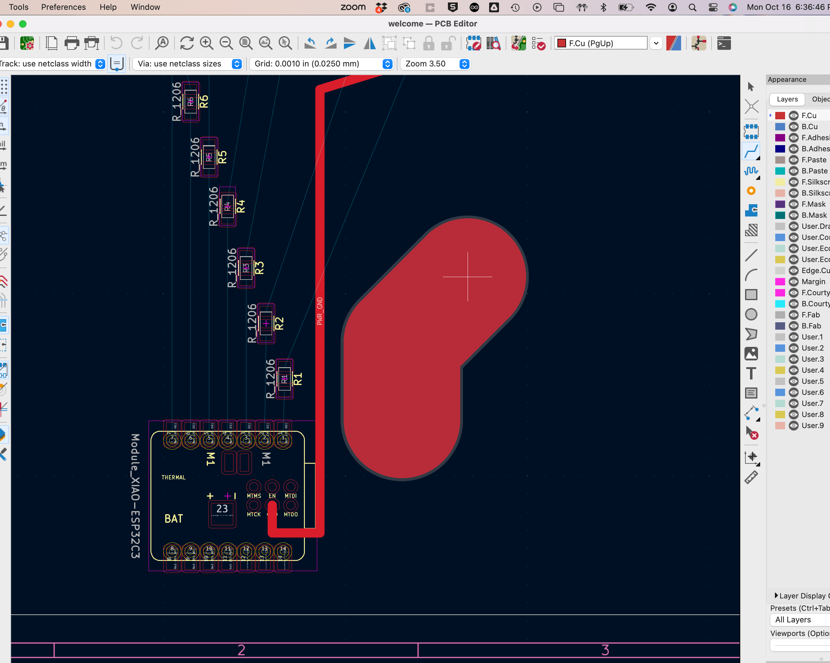
My group characterized our design rules for our in-house PCB production process and sent a PCB out to a board house.
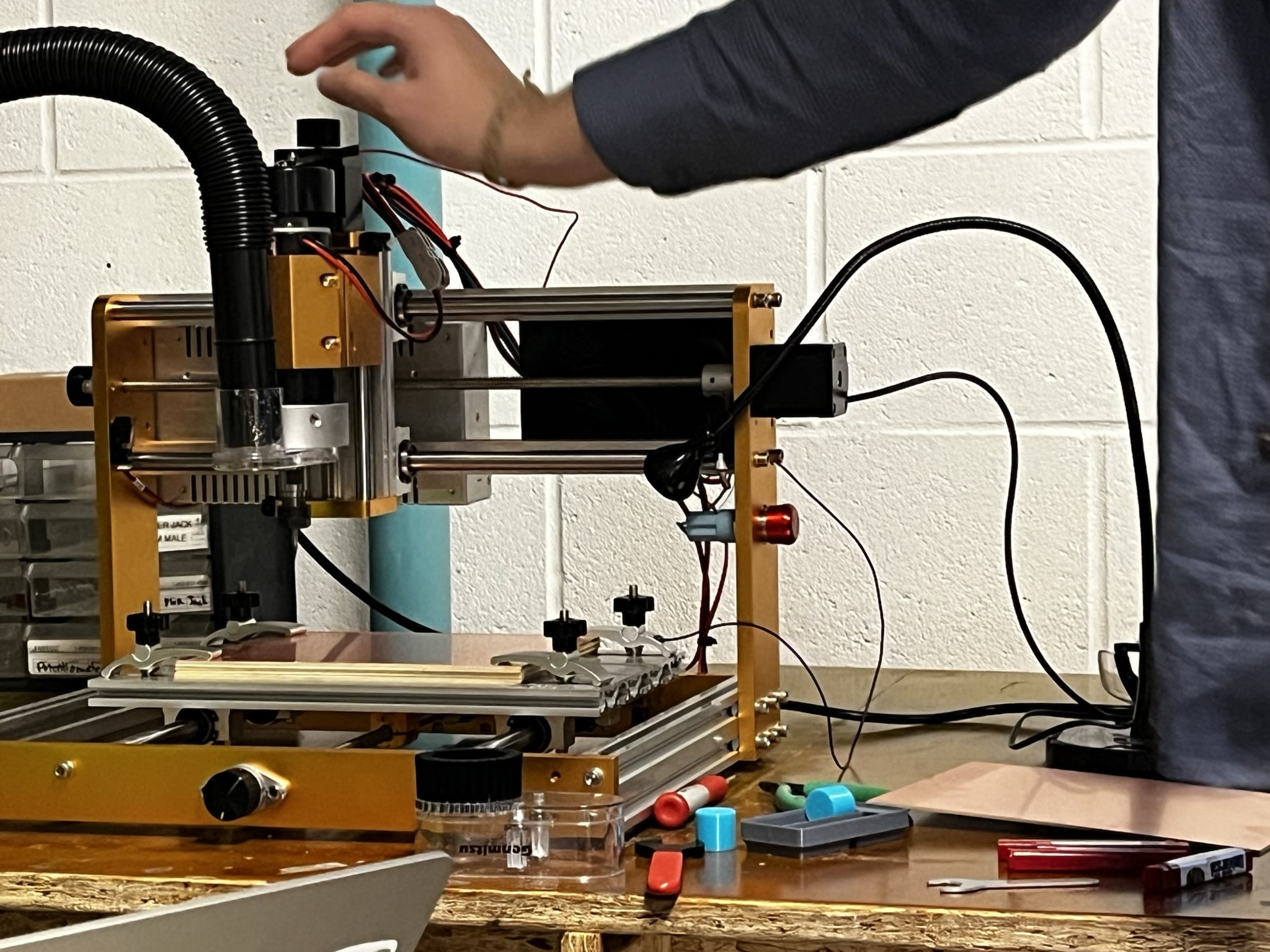
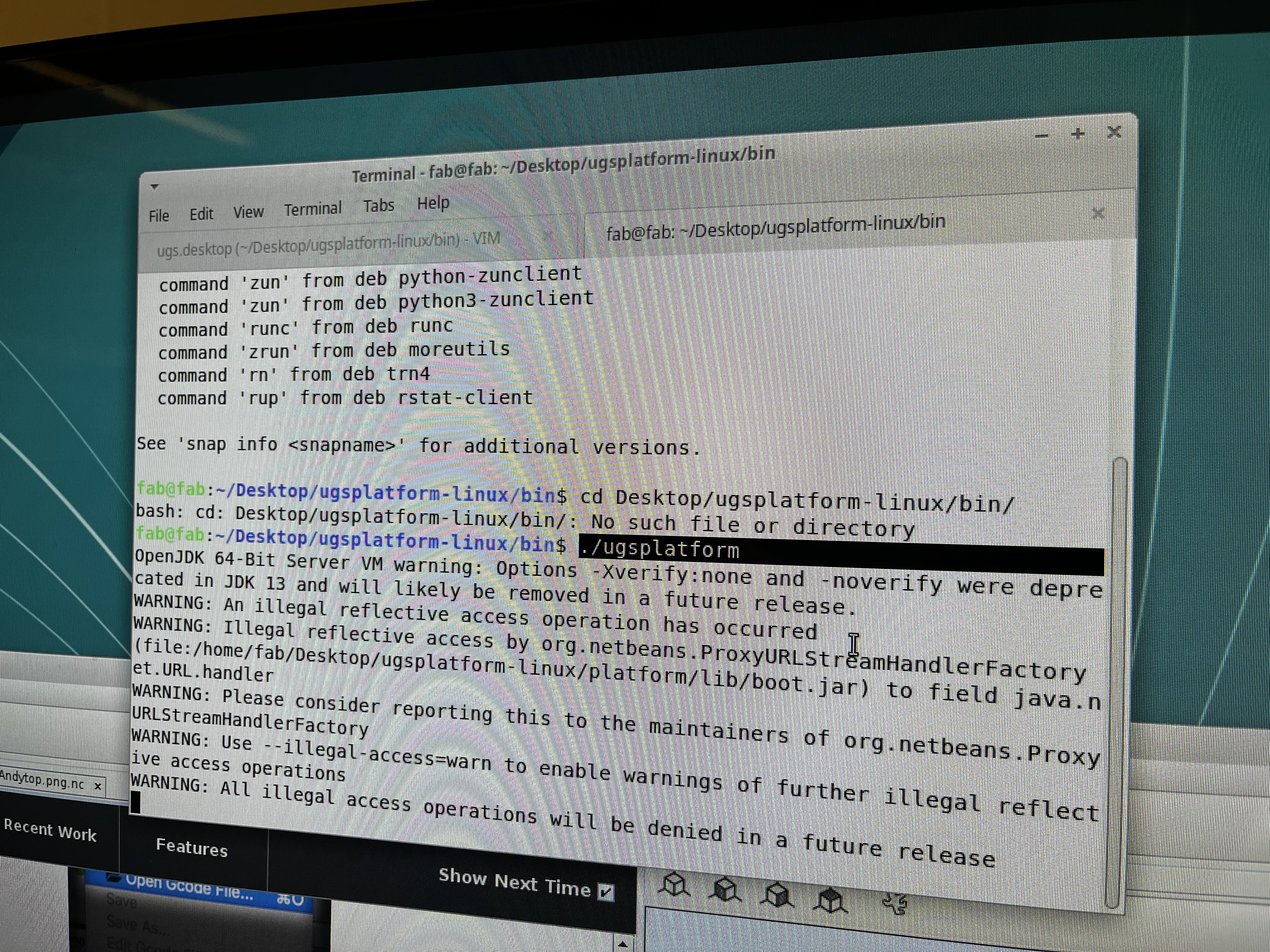
I was deciding between using the Metropolis Other Mill or CBA Mill, and ended up having to use the CBA one because my design was big. Learning to mill a PCB was an exciting journey that combined creativity, precision, and a bit of technical know-how. My goal was to create a custom PCB for a small electronics project I had in mind, and milling seemed like a cost-effective and hands-on approach. First, I familiarized myself with the basics of PCB design using KiCad. Understanding the design principles, such as component placement, trace routing, and designing a schematic, was crucial before moving on to the milling process. Once I had a design ready, I exported the PCB layout in a format compatible with the milling machine, usually Gerber or G-code files. This step was pivotal, as any errors in the design could result in a faulty PCB. Next, I set up the milling machine, ensuring it was calibrated correctly and had the appropriate cutting tools installed. Precision was key at this stage, as even a slight misalignment could affect the final outcome. I carefully loaded the PCB material, usually a copper-clad board, into the machine and secured it in place. Following the instructions, I set the milling parameters such as depth of cut, spindle speed, and feed rate based on the specifics of my design and the capabilities of the machine. Once everything was set up, I initiated the milling process. The machine began cutting away the excess copper, leaving behind the traces and pads as per my design. It was fascinating to watch the machine meticulously follow the paths outlined in the design file. After the milling was complete, I carefully removed the milled PCB from the machine and inspected it for any errors or imperfections. Any leftover copper bits were cleaned off, and the PCB was examined under a magnifying glass to ensure the traces were well-defined and there were no unwanted breaks. Overall, learning to mill a PCB was a rewarding experience that required attention to detail, patience, and a willingness to learn and adapt throughout the process. It allowed me to turn my design ideas into a tangible, functional circuit board for my projects.


-min.png)