Week 6 - Group Assignment Summary
CNC Router Characterization & Design Rules
Assignment Overview
This page summarizes the group assignment for Week 7, focusing on characterizing the design rules for the EECS shop CNC router through systematic testing of runout, alignment, fixturing, speeds, feeds, materials, and toolpaths. This comprehensive assignment provides essential hands-on experience with CNC machining capabilities and manufacturing parameters.
Group Assignment: EECS Shop CNC Router Characterization
Characterize the design rules for the EECS shop CNC router through systematic testing of runout, alignment, fixturing, speeds, feeds, materials, and toolpaths.
Characterization Parameters
Comprehensive testing of CNC router capabilities to establish design rules and manufacturing parameters for successful machining operations.
Reference Materials
Source: MIT HTMAA Slack Discussion
Detailed notes from Anthony's training session on CNC router characterization and design rules
Critical Parameters for Characterization
- Runout: Tool concentricity deviation affecting kerf width and dimensional accuracy
- Alignment: Workpiece positioning accuracy for final part dimensional control
- Fixturing: Workholding methods using plastic/steel nails for secure stock positioning
- Speeds & Feeds: Optimized parameters balancing tool life, material removal, and surface finish
- Materials: OSB only (other materials require approval and additional cost)
- Toolpath Generation: 3HP spindle (2.2kW) with strict safety protocols
Expert Guidelines from Anthony
Design & Joints
- OSB Joints: Slots and tabs optimal; other joints challenging due to material structure
- Component Strategy: Design joints in-place; create components from bodies for joint features
- Finishing: File/rasp for non-filletable edges; expect multiple days for sanding
Tooling & Safety
- Tool Selection: Two-tool strategy: small for detail, large for rough cuts
- Safety Protocol: No jewelry/loose items; secure tool mounting critical
- Preparation: Arrive with CAD complete and CAM attempted; post-process before machining
⚠️ Critical Safety Note
Tool Security: Fires can occur from excessive depth or steep angles. Previous incidents involved frame contact. Always verify tool tightness before operation.
Post-Processing Check: Verify TAB_FIT_CHECK, tool diameter, corner radius (cr), and minimum height (zmin) parameters.
EECS Shop CNC Router Design Rules
Succinct guidelines derived from our characterization to ensure predictable outcomes on the EECS shop CNC router.
Runout
Measured at the tool: joints loosen with usage; fresh cuts are tighter.
| Metric | Value (in) |
|---|---|
| Average runout | 0.0036 |
| Standard deviation | 0.0020 |
| Median (freshly machined) | 0.0020 |
Use average + 1σ (~0.0056 in) as a conservative clearance allowance for press fits that will be tested repeatedly.
Dial/runout measurement indicating consistent concentricity with slight loosening after fit tests.
Clearance
Press-fit clearance tests across increments; loosened joints increase effective clearance over time.
| Peg length [in] | Hole size [in] | Clearance [in] | Joint type | Fit type |
|---|---|---|---|---|
| 1.995 | 2 | -0.005 | Interference | Press |
| 2 | 2 | 0 | Line-to-line | Transition |
| 2.005 | 2 | 0.005 | Clearance | Slip |
Use 0.005 in clearance for slip fits; interference fits require press assembly.
Clearance measurement setup showing press-fit testing across different peg sizes and hole clearances.
Full Runout Measurements
| Measurement | Value [in] | Notes |
|---|---|---|
| Fresh cut 1 | 0.002 | Initial measurement |
| Fresh cut 2 | 0.002 | Consistent |
| After fit test 1 | 0.004 | Joint loosening |
| After fit test 2 | 0.005 | Increased wear |
| After fit test 3 | 0.006 | Maximum observed |
Full Clearance Measurements
| Test | Peg [in] | Hole [in] | Result |
|---|---|---|---|
| Tight fit | 1.995 | 2.000 | Press required |
| Nominal | 2.000 | 2.000 | Snug fit |
| Loose fit | 2.005 | 2.000 | Slip fit |
Alignment
- Square stock to the bed; use probe to set origin at stock bottom-left.
- Match this origin in Fusion CAM manufacturing setup.
Fixturing
- Use plastic nails via plastic nail gun; place outside final contours where possible.
- Removal: crowbar to pop parts; slide to shear remaining nails; clean all nails from bed.
Speeds & Feeds
- Spindle: 10,000 RPM; Feed: 90–100 in/min; other values per Fusion defaults.
- Reference video: Anthony's CAM tutorial.
Materials
- OSB only. Other materials require prior approval and incur additional cost.
Toolpath Generation (Fusion CAM)
- Create a manufacturing model; convert bodies to components.
- Sketch stock size; use Arrange to nest components within the stock.
- Create a manufacturing setup aligned to stock bottom-left origin.
- Define parameters for each tool. Use two 2D contour toolpaths:
- 3/8 in (0.375) tool for primary contours.
- 1/4 in (0.25) tool for detail features.
- Simulate, post-process, and export for the router as required.
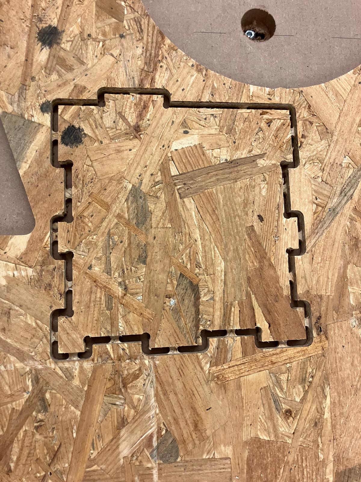
Systematic Test Part Design
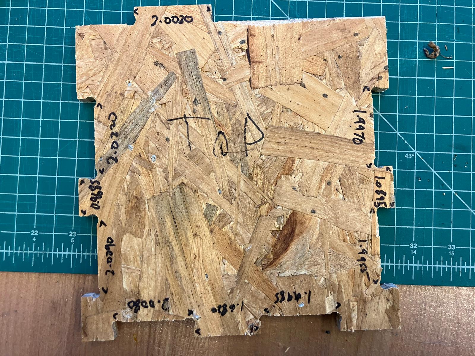
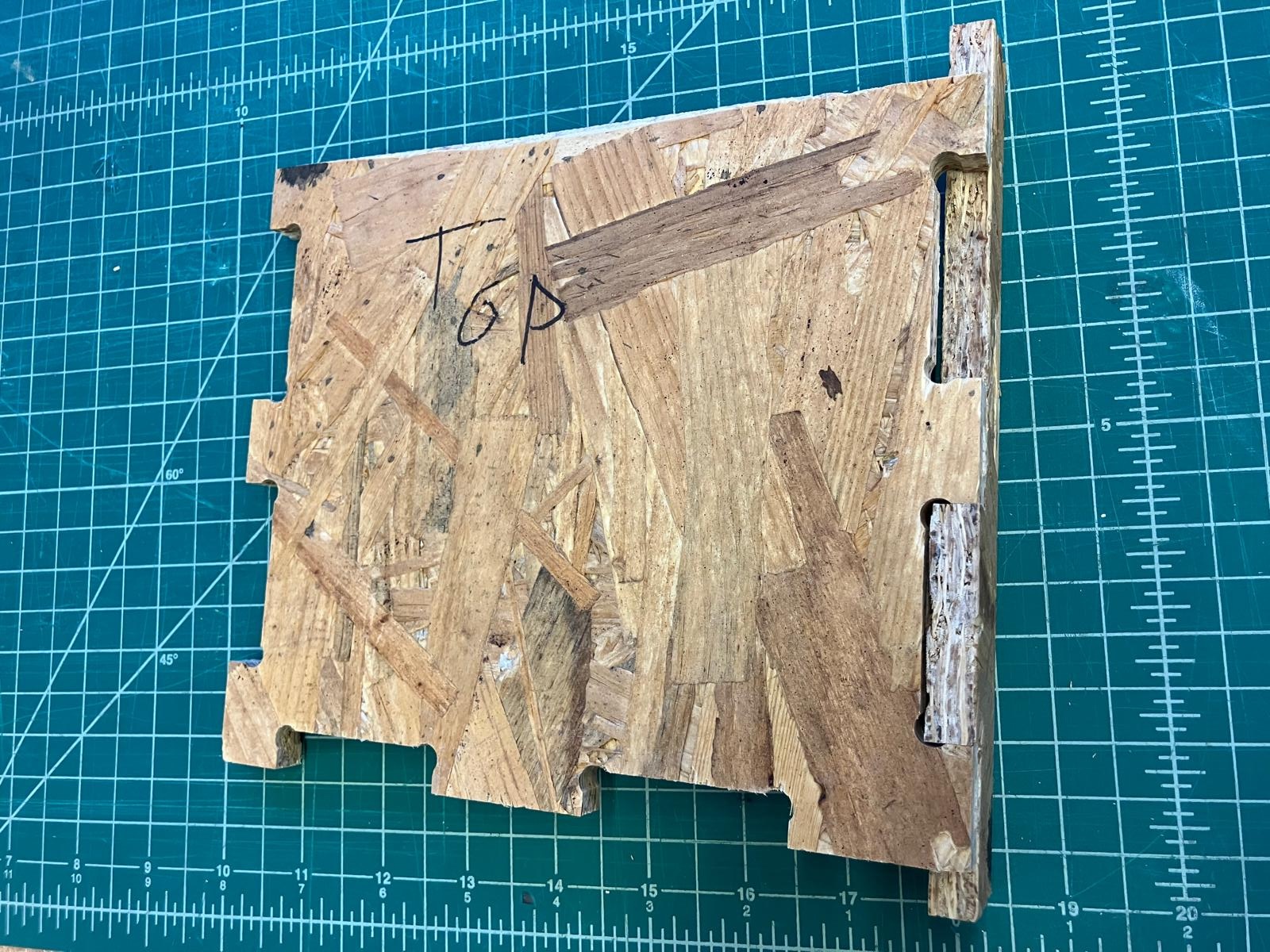
Designed test part featuring 2-inch slots with 0.005" incremental clearances to systematically evaluate joint tolerances and press-fit characteristics.
Press Fit Clearance Matrix
-0.005"
Tight Fit
0.000"
Nominal
+0.005"
Loose Fit
Manufacturing Process Documentation
Systematic documentation of the CNC router characterization process from design to measurement, capturing key parameters for design rule establishment.
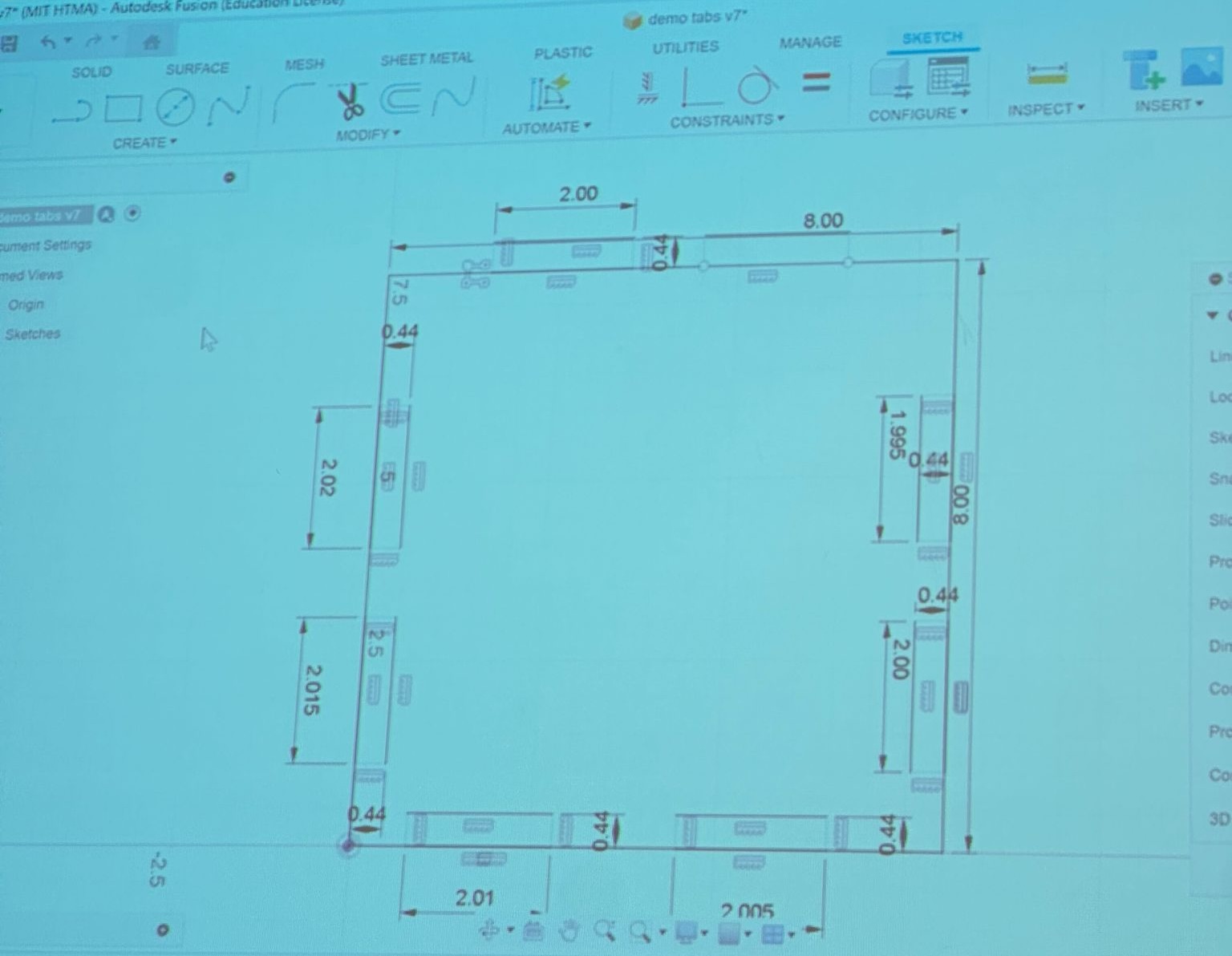
Demo tabs design featuring 2-inch slots with 0.005" clearance increments for systematic joint tolerance testing
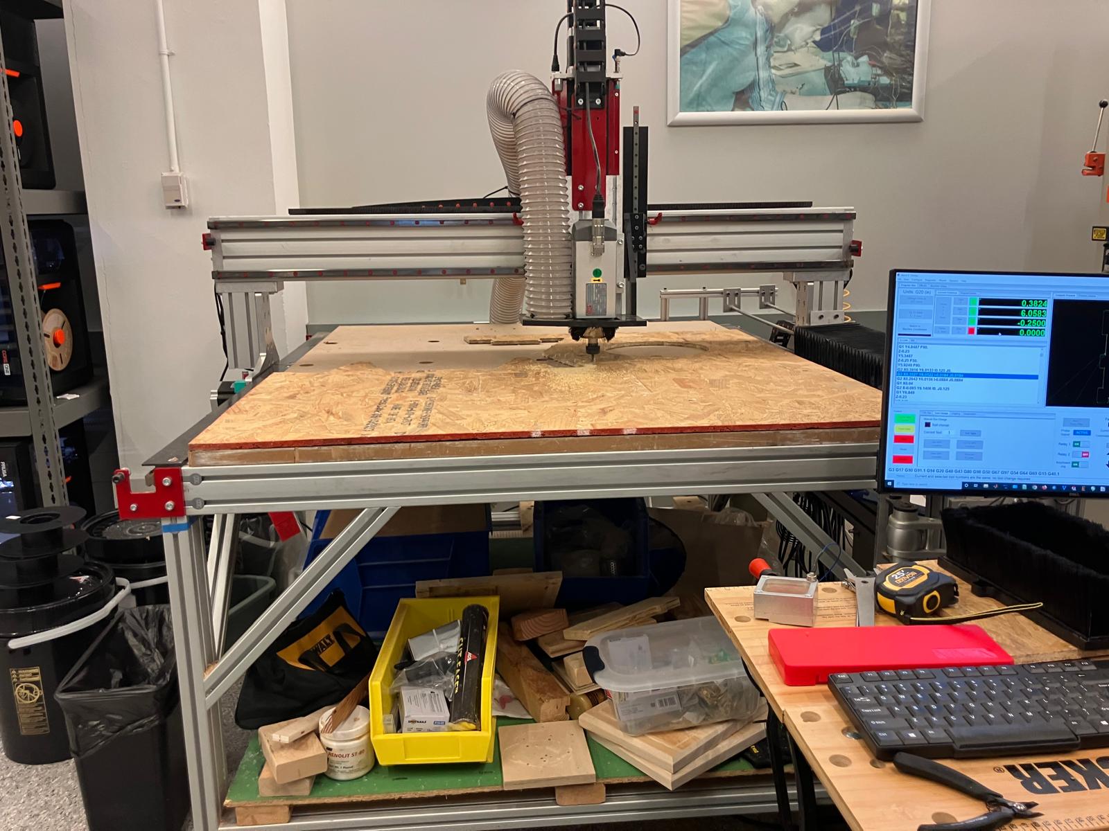
CNC router executing characterization cuts with 3HP spindle at optimized speeds and feeds for OSB material
Completed test part showing three joint clearance variations (1.995", 2.000", 2.005") for press-fit tolerance analysis
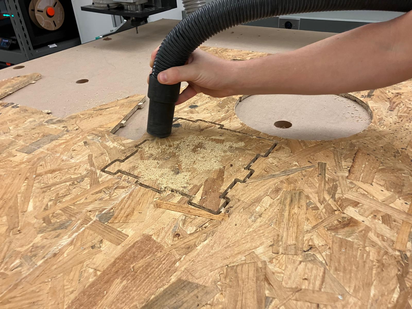
Post-machining cleanup using vacuum system to remove OSB dust and debris from work area and test parts
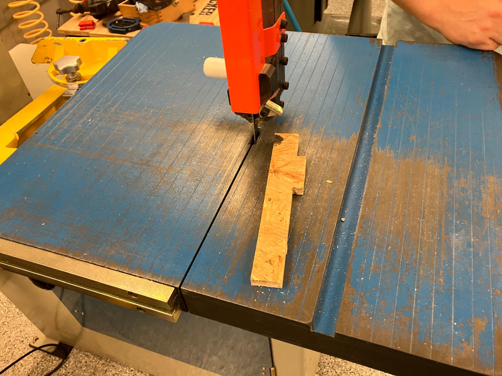
Bandsaw cutting for part separation and precision measurement using calipers to determine actual joint clearances and runout characteristics
Design Files
Demo Tabs v8.f3d: Complete Fusion 360 design file for CNC router characterization test parts with various joint clearances and tab configurations.
Characterization Completion Checklist
Priority Action: Measure runout using calipers based on test part design, then systematically complete all characterization parameters.
Measurement & Analysis
- ✓ Measure runout with calipers
- ✓ Complete alignment testing
- ✓ Document dimensional accuracy
Process Validation
- ✓ Verify fixturing methods
- ✓ Document speeds and feeds
- ✓ Validate toolpath generation
Full Assignment Details
For complete details on the Week 6 group assignment, including comprehensive CNC router characterization, design rules, and detailed results, please visit the full assignment page.
🔗 View Full Week 6 Group Assignment DetailsSpecial Thanks to Our Section
We would like to express our sincere gratitude to all members of our section for their invaluable collaboration throughout this group assignment. Your contributions were essential to the success of this comprehensive CNC router characterization project.
Collaboration Activities
- Design rule documentation and measurement
- Manufacturing process analysis and characterization
- CNC router testing and parameter optimization
- Quality control procedure development
Knowledge Sharing
- CNC machining best practices and guidelines
- Manufacturing process limitations and capabilities
- Quality control methodologies and testing
- Professional manufacturing workflows
This collaborative effort demonstrates the power of teamwork in technical education and hands-on learning. The collective knowledge and shared experiences significantly enhanced our understanding of CNC machining processes and design optimization strategies.
References
- CNC Design Guidelines
Industry standards and best practices for CNC machining and manufacturing - Manufacturing Process Documentation
In-house fabrication procedures and equipment specifications - CNC Router Specifications
Professional manufacturing capabilities and design rule requirements - Safety Standards
OSHA and related standards for CNC machining safety and manufacturing - Design for Manufacturing (DFM)
Guidelines for optimizing designs for manufacturability and cost
Ethical AI Use
Documentation of AI tool usage for this week's group assignment summary and website development work.
Week 7 - Group Assignment Summary Development
This session covers the development of the Week 7 page for the CNC router characterization group assignment, including content structure, technical documentation, and comprehensive coverage of CNC machining processes.
AI Development Documentation
Complete development transcript documenting the AI-assisted creation of the Week 7 group assignment page, including content structure, technical documentation, and website development process.
Key AI Activities
- Content Structure
Creation of comprehensive HTML structure for CNC machining documentation - Technical Documentation
Development of detailed sections covering design rules and manufacturing processes - Process Integration
Implementation of CNC router characterization and manufacturing workflow information - Navigation Integration
Addition of Week 7 link to main index page for seamless course navigation - Week 6 Summary Integration
Extraction and integration of Week 6 group assignment content into Week 7 page - Image Integration
Integration of key images from week6groupassignment folder with proper styling and captions - Link Integration
Addition of external link to full Week 6 assignment details with proper accessibility attributes
AI Tools Used
- Cursor AI
Code generation, content structuring, and website development assistance - Technical Content Generation
Creation of comprehensive CNC machining process documentation - Website Design
Implementation of consistent styling and responsive layout - Content Integration
Seamless integration of Week 6 content into Week 7 page structure - Image Processing
Integration and styling of process images with proper responsive layouts