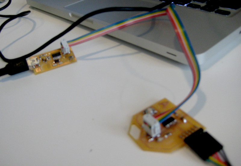
Week 6: Electronics Design
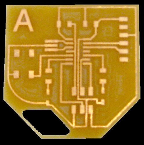
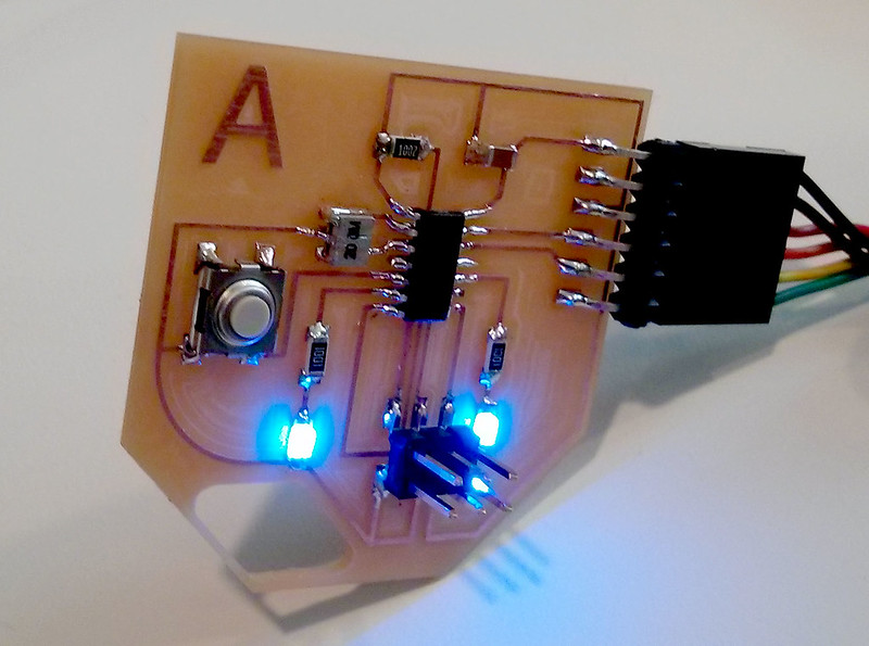
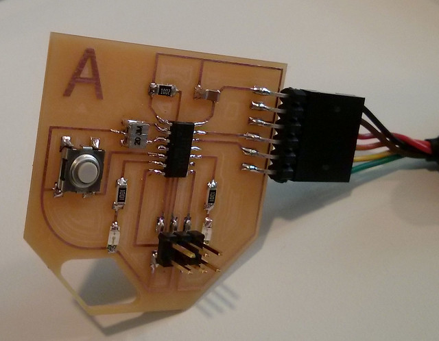
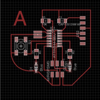
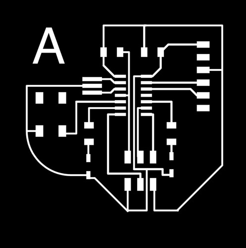
This week I learnt how to design a PCB using Eagle software. I redrew the echo hello-world board. I modified the circuit design by adding 2 LEDs and a switch.
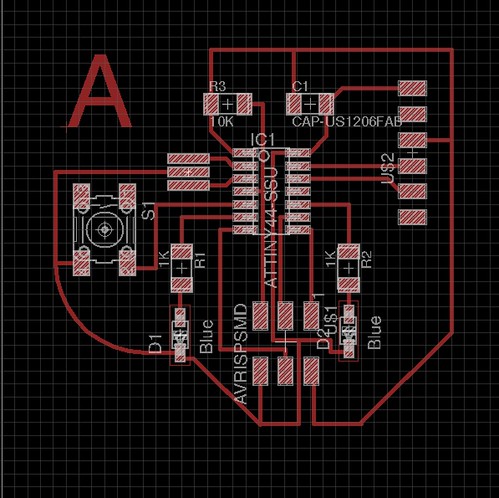
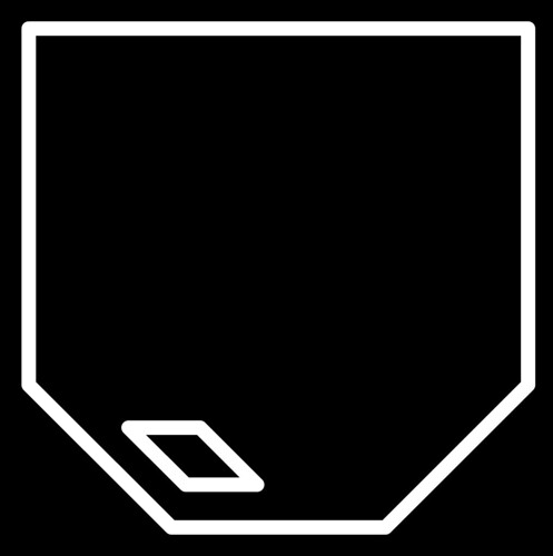
In the process I also learnt the basics of electronics. Routing the board was a bit challenging for me. I spent a lot of time figuring out how to use Eagle. I wanted to draw the board in paisley shape but didn’t know how to make precise curved shapes using eagle. So I ended up making a polygon shaped board.
Redrawing the Schematic in Eagle
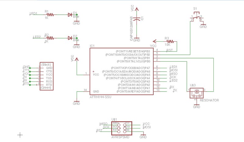
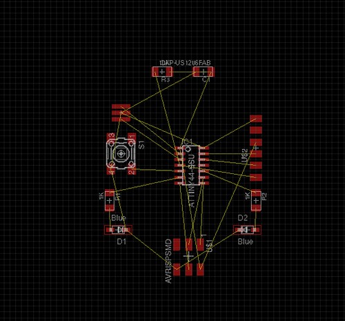
Drawing the schematic helped me understand the electronic components and connections. Also David helped me understand some electronics concepts.I added the components using fab library. I used this tutorial to draw schematic in eagle. I connected two LEDs using 1K resistor in series and added a switch to the original design.
I loved the Label option and it was helpful to avoid wire overlap in the connections.
Creating the circuit layout
This was the most difficult and time consuming step. I first placed all the components together matching the closest connections and then started making traces.
There were lots of overlaps and I spent almost 3 hours drawing traces. I found out later that Eagle allows you to draw curved traces.
I might try redrawing the hello board in paisley shape in future.
After making traces I used the DSR (Design rules) option on the left toolbar to check if my circuit was okay. In clearance menu I kept 16 mill the minimum clearance between objects.
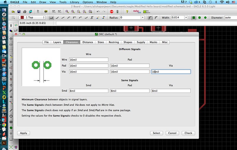
It showed me some errors when I checked the clearance. So I changed my traces width from 0.016 to 0.014 to make sure I had enough space between wires and pads.
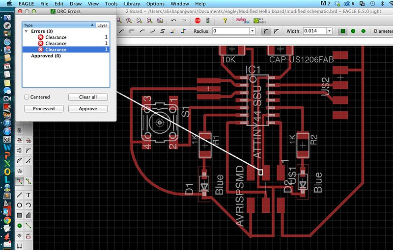
After making traces I used the DSR (Design rules) option on the left toolbar to check if my circuit was okay. In clearance menu I kept 16 mill the minimum clearance between objects.
It showed me some errors when I checked the clearance. So I changed my traces width from 0.016 to 0.014 to make sure I had enough space between wires and pads.
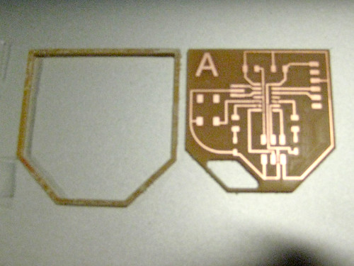
Exporting as png files
I exported traces and outline as PNG files with a 2000 dpi resolution. After exporting I realized that I should have drawn the outline of the board on the dimension layer and not on the Milling layer
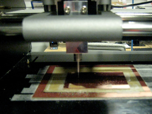
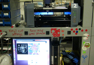
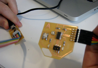
Milling and stuffing the board
I used the same steps as week 3. My outer dimension layer was too thick so when I sent the command to modela milling machine, it milled a separate border as the outline.