 |
||||||||||||
| HOW TO MAKE (ALMOST) ANYTHING MIT MEDIA LAB |
|
PROJECTS | ABOUT | CONTACT | ||||||||
|
|
|||||||||||
| ELECTRONICS DESIGN - week6 | ||||||||||||
At a first glance, this week's assignment was not much different from week 3, but there was much more back-end understanding of what these circuit boards are doing. I very much liked my guru's analogy that current is like water, except that it flows uphill. The roles of the capacitor, the resistor, the resonator (=crystal) were explained to me. Time appeared as a central factor to the whole process. And, of course, instead of just downloading an image, I let Eagle generate the image for me after inserting and connecting all the components from scratch. There were two tutorials from previous years that I found most helpful: one was Dan Novy's write up from 2011, another was the Providence FabLab Tutorial. |
||||||||||||
 |
||||||||||||
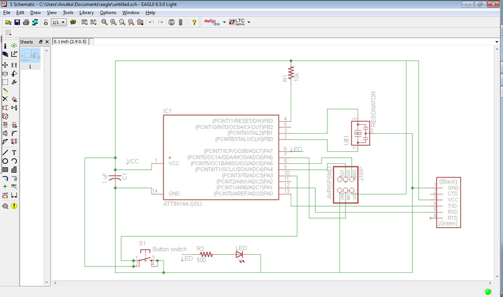
| The Eagle Schematic | ||||||||||||
|
Some important things to keep in mind when drawing the schematic:
.The Schematic is a conceptual representation of the board; the geometry of the parts and lines does not matter
as long as it connects the right parts to each other.
.Don't forget to use the Junction (the fat green dot) to signify 3+ wires intersecting as opposed to just wires happening to cross in
this conceptual space but not the geometric space.
.Instead of drawing all the lines out, can draw a wire out of a part and *name* it (via either typing in "name" into the command
line or with a button in the panel) with X, and then do the same for the other part that wire is supposed to connect to. Note that "naming" is
different from "labelling", the latter of which is just for the user to view the name. The name will tell the program to connect two wires
together if they are both named X.
|
||||||||||||
 |
||||||||||||
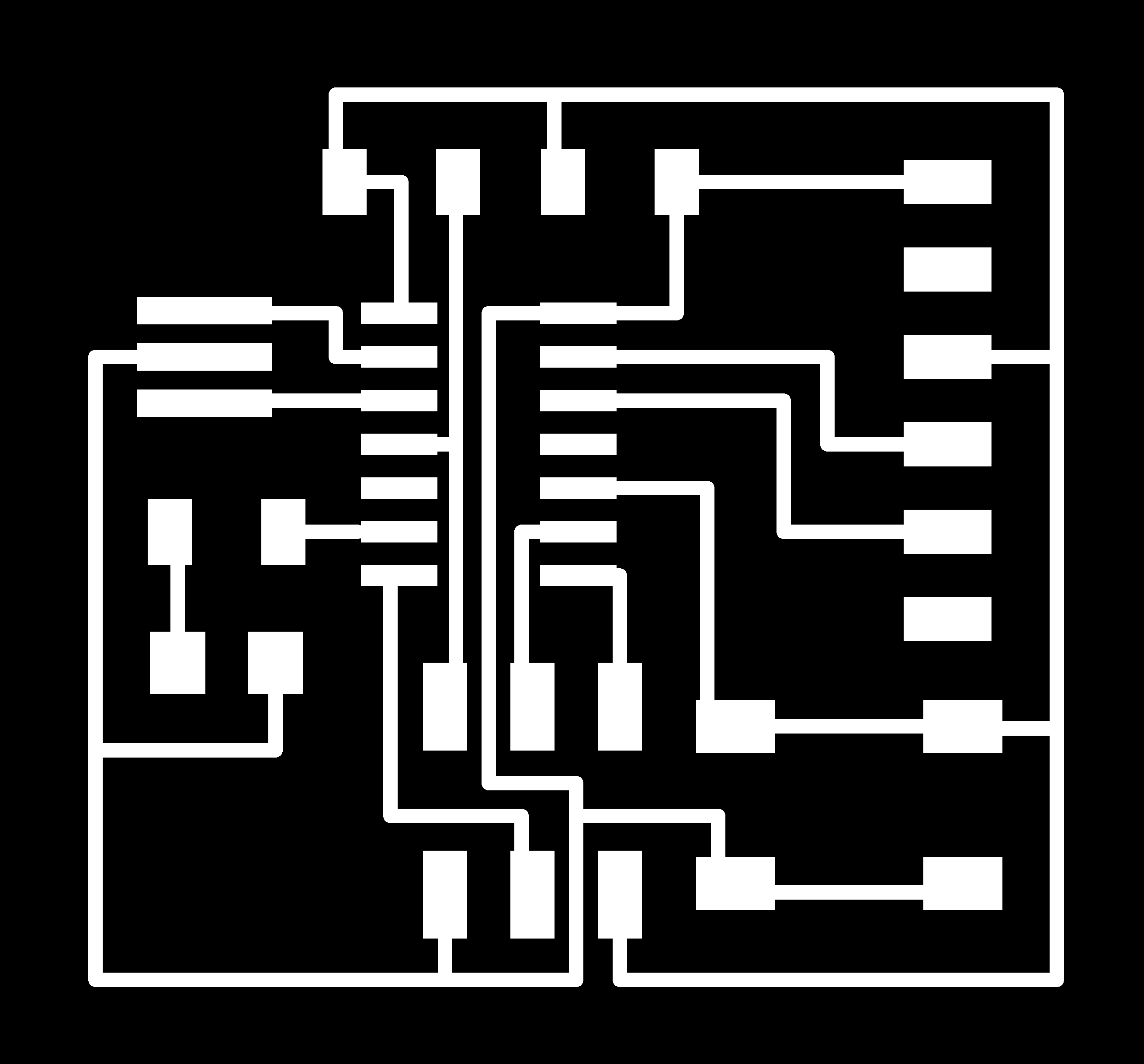
| The Eagle Board outline | ||||||||||||
 |
||||||||||||
| The Full Eagle Board | ||||||||||||
|
Some important things to keep in mind when making the Board in Eagle:
.If it turns out that you must cross wires and there is no way around it, can add a zero-Ohm resistor an an unwanted junction
to essentially "jump" one wire over another. Avoid doing this if possible, as too many unnecessary "jumps" probably just means you didn't try
that hard to avoid them.
.Don't forget to use layers (especially outline the Dimension with a different layer), and don't forget to display just select layers when Exporting to image file. If needed, invert b/w colors under Options
--> User Interface.
.When doing Design rule check and Error Check (both under 'Tools'), it is ok to ignore errors of Overlap and Stop Mask. In fact,
the software can not like some alignment that you can use your judgment to override instead of spending countless hours figuring out what was it
that bothered the Eagle's sensitive soul.
.When exporting the image, must use 2000+ dpi.
|
||||||||||||
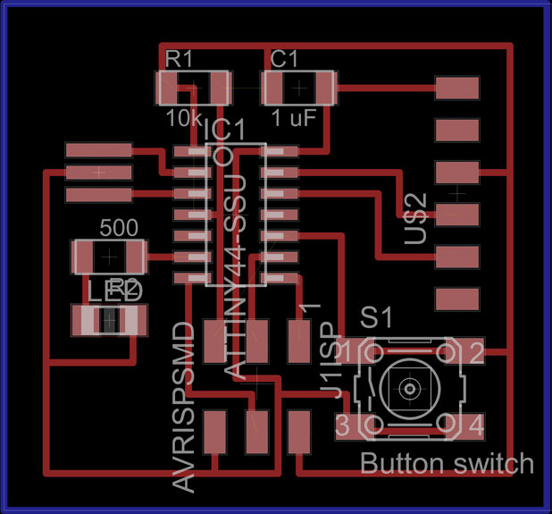
| Milling on the Modela | ||||||||||||
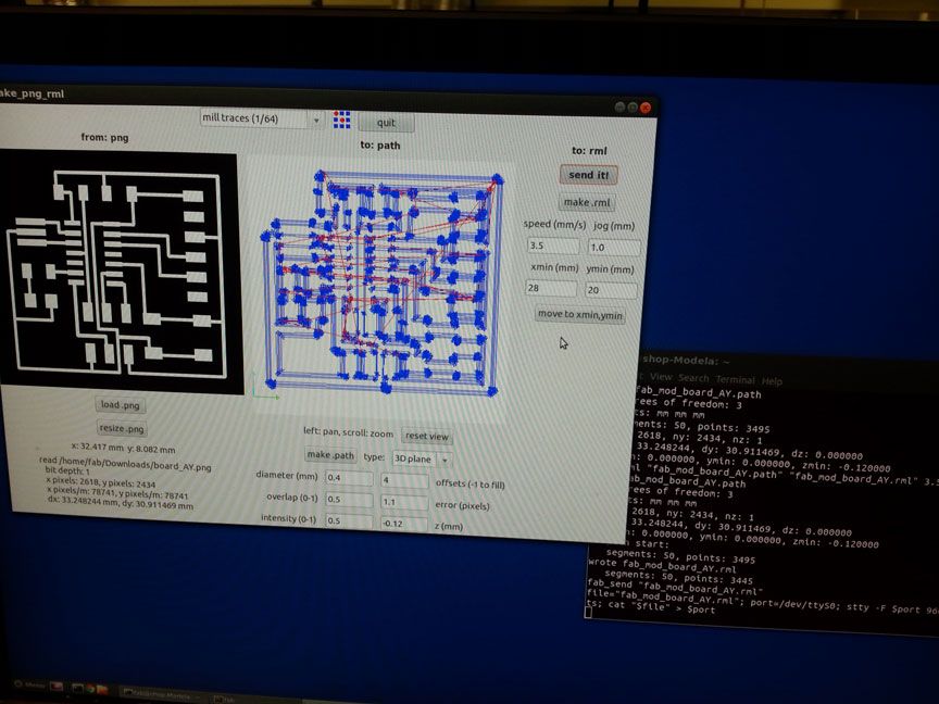
| The process was not much different from milling the first board in week3, see the image of the settings used for tracing: | ||||||||||||
 |
||||||||||||
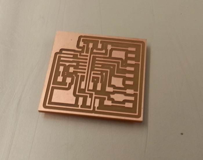
| The settings for the dimension layer (the rectangle) were a bit problematic. Likely because the lines on the edges in my file were too narrow (which I couldn't figure out how to change?), Modela milled the top and bottom lines of the rectangle but not the sides! I ended up having to lower the Diameter to 0.45mm (from 0.79mm) to allow the fab module to draw a path and Modela to actually recognize the sides as lines and to cut out the full rectangle, not just half of its sides. Other settings were all the same. Here is the final product of the milling: | ||||||||||||
 |
||||||||||||
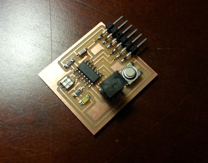
| The soldering was rather uneventful. The copper ribbon again came to the rescue, and I think I was starting to notice an art in this soldering business, particularly in the fumes of hot iron on flux. Here is the final product, not yet tested: | ||||||||||||
 |
||||||||||||
| Next... | ||||||||||||
| ...Programming! | ||||||||||||
| Copyright 2013 by Anya Yermakova | ||||||||||||