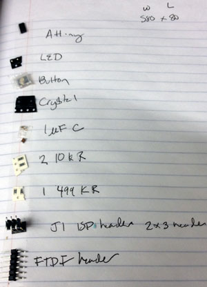
The assignment is to modify the hello ISP to include an LED and a switch. The circuit board needs to be milled using the Modela, or vinyl cutter. All components need to be located and placed on the board. Time permitting the board needs to be programmed so it can blink when the button is depressed. Nothing is better for depression than light!!
This week we are designing and making our very own circuit boards! How fun is that! I get to work with lead, copper, machines and scorching heat! I created a few stained glass panels many years ago and this was my only previous experience soldering. So I thought, how hard can soldering a circuit board be? It is much much smaller. Not quite the same. Having soldered the circuit board earlier in the semester I was excited to practice soldering and milling again to improve my soldering skills!
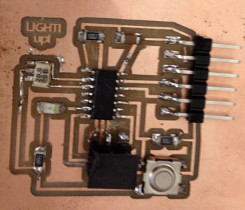
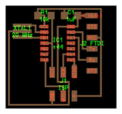
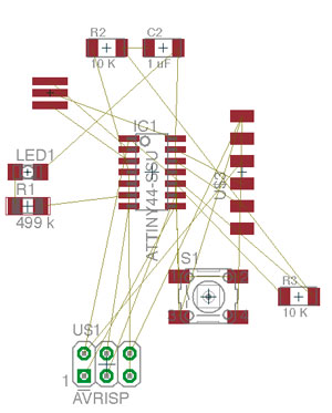
I downloaded the freeware version of Eagle to layout my board. Incidentally the board I am modifying is Neil's helloISP shown here:
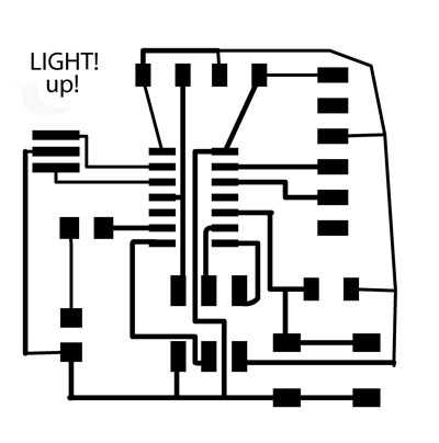
Here is the layout in Eagle with button and LED added. I looked at a lot of past student websites to see their designs and to see which components to use..
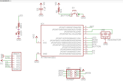
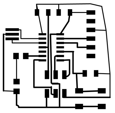
The software isn't that difficult to use so far, but at this stage I am just finding and placing components and relabeling them. The most difficult part is finding the right components to add. Searching through tons of switches to find the right one can be overwhelming. Next I need to add connections. Luckily our TA said if you label all of the connections the wiring will be done for you. I am going to try that out and export the file as a png. Here is the result when switching to the board format. What a mess! Far less than ideal. Will require some tweaking by hand before exporting as a png and milling out.
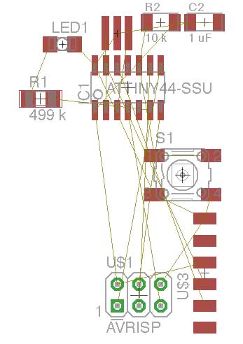
After using the ratsnest tool to figure out the wire connections, using the autorouter, and moving around all components and wires around by hand I get a solution with 3 errors. I have 3 overlaps. I could deal with these by adding 0 ohm resistors and making a 1.5D board? I also removed the pull up resistor attached to the switch because there is an internal pull up resistor in the microprocessor. Moving the wires by hand I wasn't certain if I accidentally connected things that should not be? I also ripped up all of the vias that the autorouter added with the ripup tool in the board layout section. I don't know if this will be a problem later?? Here is my result, 4 hours later. I can see how people make a career out of writing autorouting software. The dots in red are where there is a wire overlap and shouldm't be.
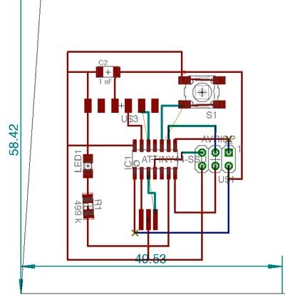
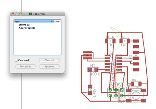
Finally no errors when doing design rule check. Rerouting this board and figuring out where to place components took over 5 hours! Am I doing something wrong here? Also am using the wrong ISP header pads. So switched to schematic view and used the replace part command to choose the correct header.
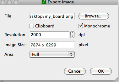
In eagle, select the layer you want to display, select export, select monochrome, set dpi to 2000 and save image.
Opened image in photoshop to create board outline and to add lettering to the board

See week 2 for additional steps.
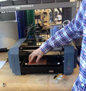
I changed the sacrificial layer of copper, cleaned everything off, loaded the png in fab modules, inverted the png, changed the cut depth to -.2. Zeroed x, y on milling machine. Placed 1/64th endmill in, Lowered z height on endmill so there was a finger tip's width in between the top and bottom so there'd be room for the endmill to move down. Zero the z height and start milling. I zeroed the board a bit too close to the edge so when I went to cut out the board I was worried that the cut out would go off the board so I left the board bigger and didn't cut it out. This de finitely should be redone.
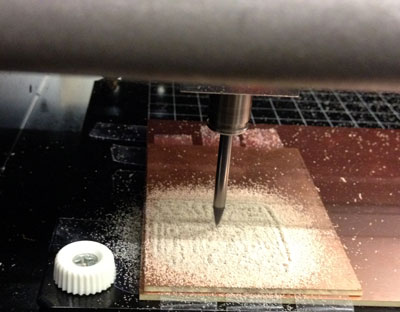
A few of the traces came out as touching so I cut away the copper to keep separation in between traces. This should be changed in my design.
Stay tuned...Week 7 for additional steps.
Copyright 2013 Kathy Sinclair