Final Project - Realtime MBTA map
So, I'll be honest, my final project has failed. It came tantalizingly close to being finishable, but due to fundamental design errors which revolved from an insufficient understanding of the fabrication tools, and a lack of time to redesign the project to be fabbable with the current tools, I'm left with a incomplete assortment of modules. Hopefully this page can serve as a sort of testament of my errors.
I'll start out my listing some of by major take aways from that I realized while building the project, a tl;dr of sorts, in the case anyone stumbles upon this page in the future:
With that brief explanation out of the way, I'll move on to discussing the actual details of my project. The project is something I've been interested in for a long time, so with any luck I can take a crack at revision 2 in the future with the knowledge I gained by failing to complete this final project.
As you might have seen in the title of this page, my idea for a final project was to make a realtime MBTA map. By taking the data on where the MBTA trains are at any given time, and then translating that to "real-space" with LEDs on a personally fabricated map, I thought I'd have a really neat piece of technological art for my apartment. Towards that goal, the MBTA provides freely accessible data on where their trains are (MBTA realtime data portal). You can register for a free API-key to access this data, which is more than sufficient for personal use. In reality, the data provided is not quite data on where the trains are exactly, but rather a timestamped velocity and heading taken when a train passed a fixed measuring device with known location that are arranged throughout the lines. My plan was to use a little bit of extrapolation using the timestamp, velocity data, and the constrained route of the train to predict the realtime location. With a bit of geometric considerations, this extrapolated realtime data could then be mapped to LEDs in physical space. Unfortunately I got hung up on the fabrication process, so the code for realtime extrapolation and mapping to physical space of train location was never completed. That being said, for my week 13 assignment, I completed a GUI proof of concept which pulled down, parsed, and plotted the realtime MBTA data.
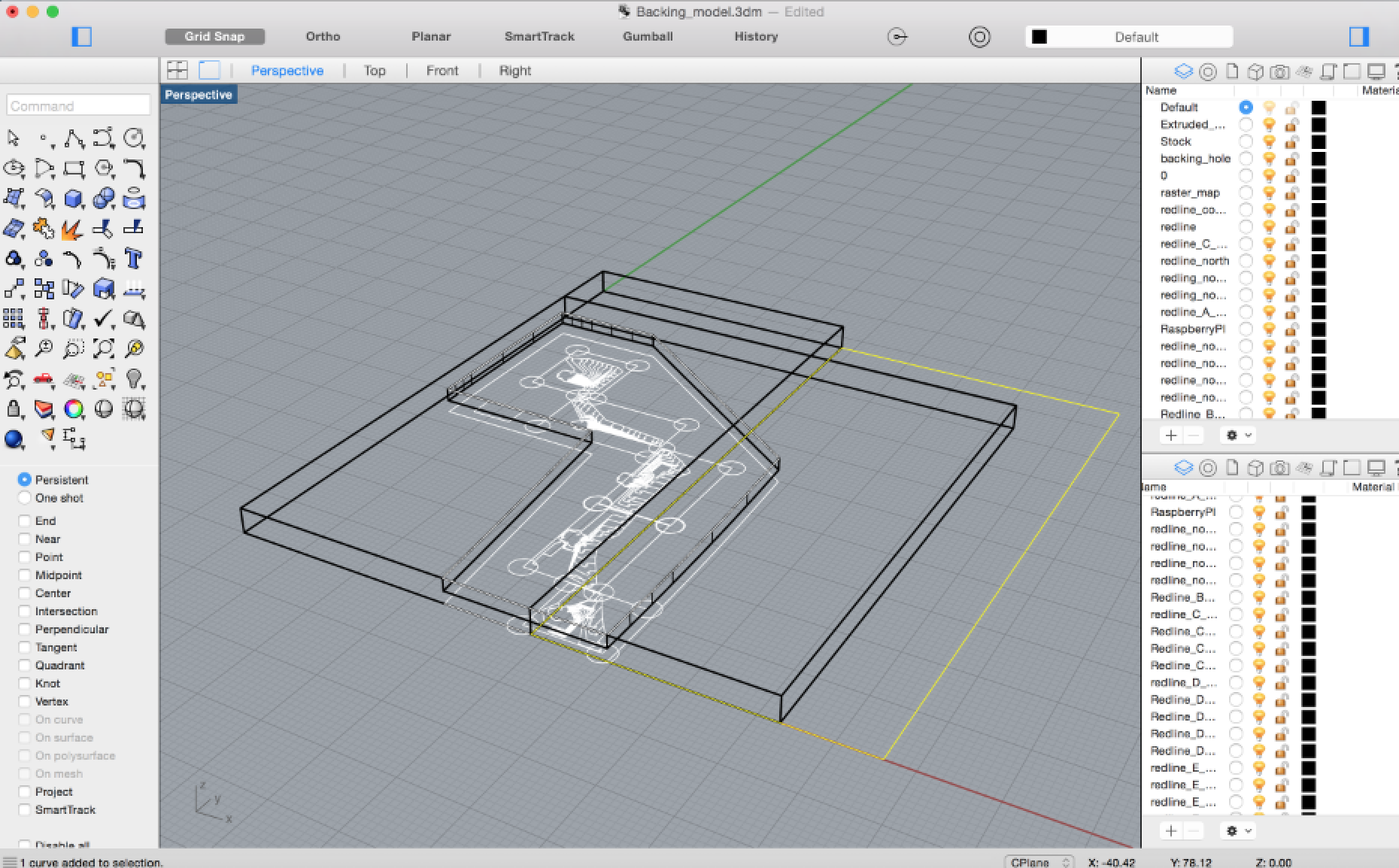
I'll summarize my efforts towards the final project with the picture below, and then give specific information on the process of each submodule beyond that:
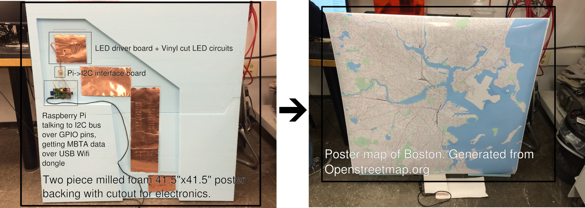
Summary of the submodules of the project, and a representation of what I was able to complete.
The big picture of this project is it is a convoluted way to fan out LEDs. These LEDs happened to have been placed in such a way that they matched the geography of Boston's subway redline, but LED lighting nonetheless. That being said, there is significant complication in "scaling up" simple tasks, largely from splitting a monolithic fabrication mode (such as modela milling), into multiple modes which need to be coordinated and registered spatially. The main submodules I used to try and accomplish this task are: Raspberry Pi (I2C controller), I2C interface and LED controller boards, vinyl cut LED fanouts, a blue foam milled backing, and a custom poster.
Raspberry Pi submodule
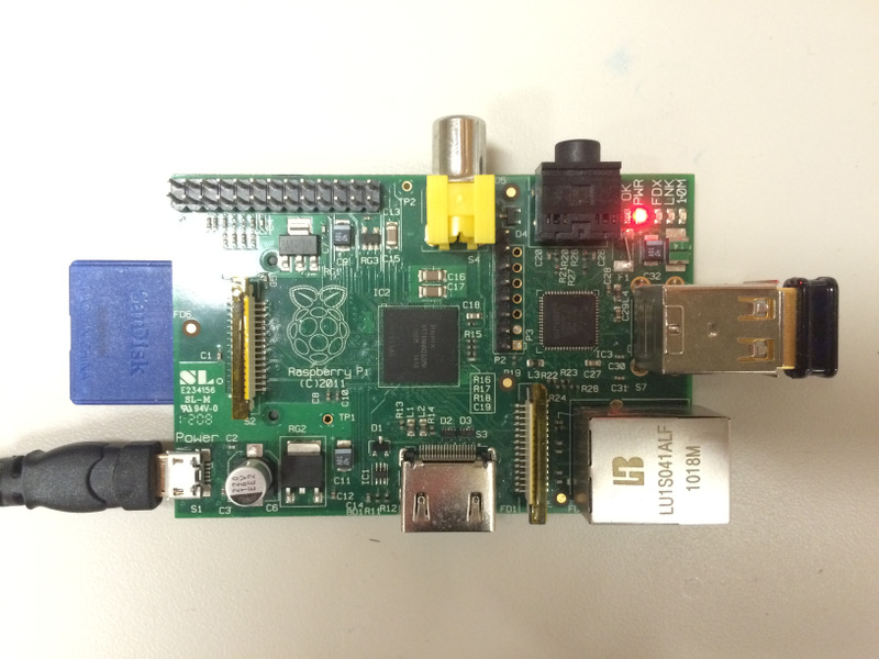
In case you haven't heard, the Raspberry Pi is a low-cost single board linux computer. At 35$ for the Model B (shown above), it is a really great tool to play around with. It is also great for electronic experimentation as it a full OS that you can program in interpreted languages (Python being my language of choice) that exposes GPIO pins to the physical world. As Neil mentioned in class, the speed on the GPIOs on the Pi (or any embedded computer), are pretty poor due to the non-realtime nature of complex operating systems. However, the Pi has built-in I2C, meaning you get the advantages of hardware timing plus the ease of Python and linux/unix to interface with your electronics. Seeing as my project required interfacing to the MBTA realtime data on the internet, the Pi was a natural choice. In my case, I've added a Wifi USB dongle to connect to the internet. A side note, the Pi I have is actually one of the earliest revision 1 Model Bs, meaning it has very limited polyfuses on the USB ports. I had to desolder a polyfuse and add a jumper wire in order for the USB dongle to be able to get enough current to work. Interested readers are challenged to find the mod in the picture above. The Raspberry Pi wiki is full of information if you want to modify you Pi in similar (or different) ways. Anyway, I chose the Pi as it let me interface data from the internet to LEDs on a board in a relatively straightforward way. I2C on the Pi is relatively straightforward, here are a couple links from the always helpful Adafruit on how to get started with I2C on the Raspbery Pi. Another note: The Raspberry Pi GPIO pins are only 3.3V resistant, don't expose them to higher voltage. For I2C, thankfully the voltage interfacing issues are a bit simplified. I2C relies on pullups to provide the "high" signal, whereas the devices on the bus assert a "low" signal by sinking current. Even if your odd I2C device on the bus is running off 5V, 3.3V on the I2C bus will still count as logic high, and the chip can still pull the line to 0V to assert logic.
In terms of software, I was coding on the Pi in Python, which lets you do everything you would need to do (including talk to I2C devices). Just have to correct to the right pins, which brings me to my next submodule...
I2C / LED driver boards
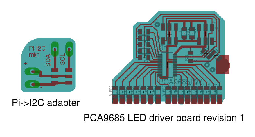
Pi->I2C board
In order to get the Pi talking to I2C, its just a matter of interfacing to the right pins. The breakout board on the left shows how I accomplished this. The Pi provides the pullup resistors on SDA and SCL, so nothing is needed other than just the physical interfacing to the 6-pin "fab" header. This 6-pin layout then became the "standard" for the I2C between my boards. This approach (including using 2 wires for 5V and GND) was inspired for this by the Gestalt boards from machine building week.
PCA9685 LED driver board revision 1
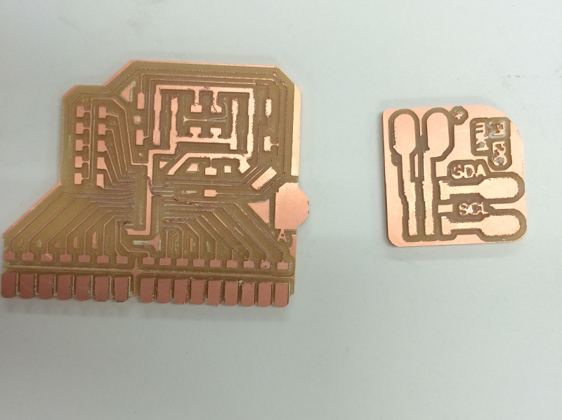
The driver board is where I first realized I had some design issues. I'll explain. First off, the part driving the board is the PCA9685, an I2C to 16-pin PWM controller. I found this part basically because I was googling "I2C LED driver", and this page came up. Seeing Adafruit's approval, I went ahead to Digikey and bought 5 of the ICs for $2.50 each. I found the Eagle library for the part, and started designing. You'll notice that I ordered the part, and then put it in Eagle, which means I didn't consider the physical reality of the part before ordering. Once I had the part in eagle, I assumed that since the pin pitch kinda looked like
the pin pitch of the Fabduino (which successfully milled on the 1/64th endmill), this part would be the same. This turned out to be a mistake. The TSSOP24 package this part came in has 0.47mm pitch, which is smaller than even what the 0.01" endmill can do. As you can see with the milling results below, they aren't pretty. The 0.01" endmill requires the Modela to be in very good shape, which it wasn't. I did spend some troubleshooting time trying to figure out how to improve the Modela milling, but between trying to complete the other parts of the project, and the Modela being extremely busy in the days up to the final exam, I didn't ever get to sit down and complete a 0.01" milled board. This works into my previous advice, don't try and mill something with the 0.01" endmill for the final project
if you've never done it. This is a Bad® idea.
Blue foam poster backing / design approach
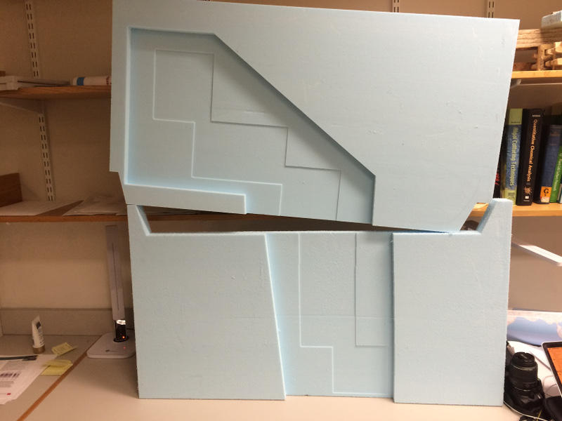
I'm actually quite happy with the way the blue foam backing turned out, if only I had the other parts to go with it. This blue foam was milled out using the Architechture Shopbot Buddy. This was after realizing on Thursday that the Onsrud I had used for 3-axis milling throughout the semester would be booked until Tuesday (after the exam). Thankfully, Enas AlKhudairy, an architechture student, stepped up to help myself and my classmate Holly with out milling on the Shopbot Buddy. Thats Enas! You were an enormous help. The backing was milled in two separate pieces (top and bottom half). The stock for each piece was 24x46x2. Basically the part fit just inside the stock, which was more luck than any part of my design:
The top part of the model was milled with an overly conservative toolpath, and so took over an hour and a half to mill. That being said, the finish is beautiful, I love my useless custom blue foam top half. However, for the bottom half, I modified the toolpath to be less conservative and it finished in 20 minutes. In between these two parts, I had to switch the stock and load the new program while Enas stepped out. I learned the hard way that if you accidentally tell the Shopbot to go to X 2000 instead of X 20, it will happily spin its motors continuously and throw the board off the machine. Thanks to an anonymous shop monitor who helped me wrangle this situation (the board almost entirely fell off the machine only twice!), I finally got my second stock on the machine, rezeroed it, and started milling.
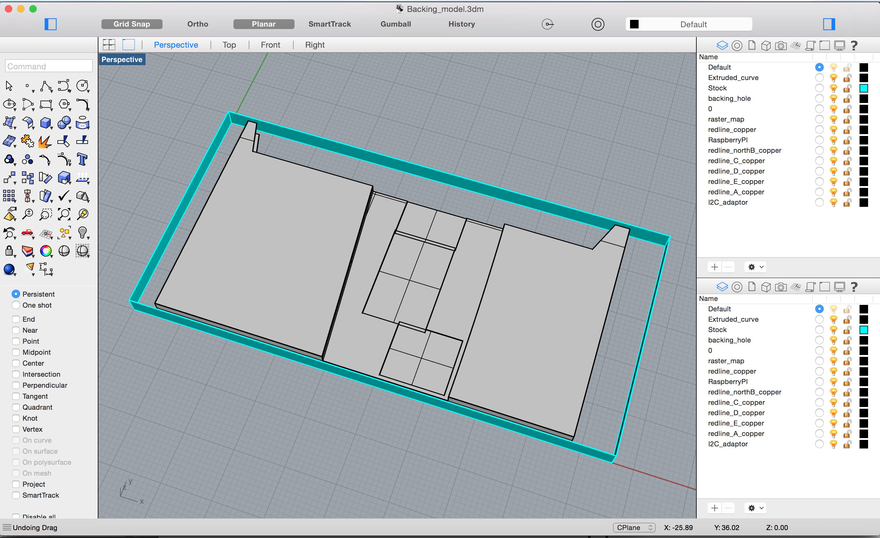
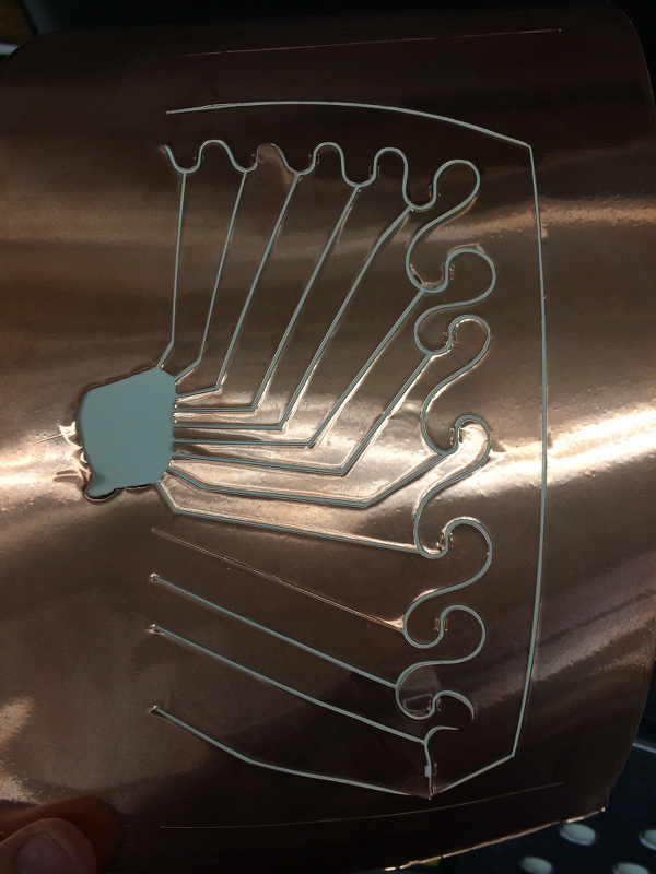
How did I design this part? As you can see from above the 3D modeling was done in Rhino. However, the majority of this project involved tracing a raster image of a map, and routing circuits around this traced raster image. To my knowledge, Rhino can't do this, so I turned to Inkscape, which at this point I am now an absolute master (for those not following along, throughout this semester I've basically shoehorned Inkscape into any possible situation as it was the "modeling" program that I knew best). Below I show my "master model" in Inkscape:
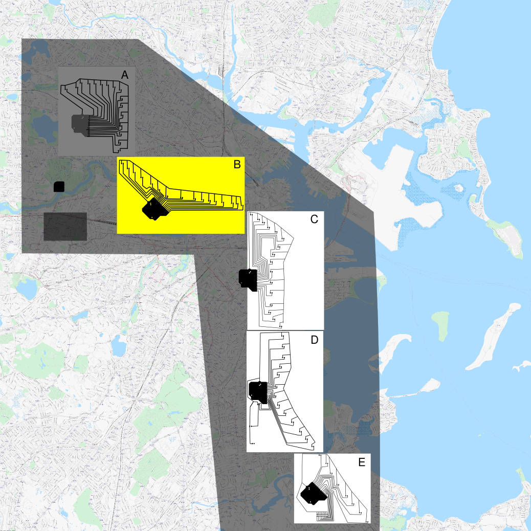
Astute readers will note that the features on my Inkscape model match the features on the blue foam. Astute readers from Boston will note that whatever that thing is, it appears to be following the Redline route. Indeed, the black traces represent both pads for LEDs and traces that go back to the PCA8695 controller board, whereas the yellow/white boxes represent the 6 inch by arbitrary of the copper stock for the vinyl cutter. How did I accomplish this? I traced the redline route and placed a bunch of pads along it, then manually drew and routed circuit traces. In order to merge the power of Inkscape and Rhino, I exported the Inkscape model and .dxf, which surprisingly actually imported into Rhino with all the layer information, letting me specify and further manipulate all the 2D curves and surfaces into a 3D form. Below I show the process of importing the .dxf.
Vinyl cut LED circuits
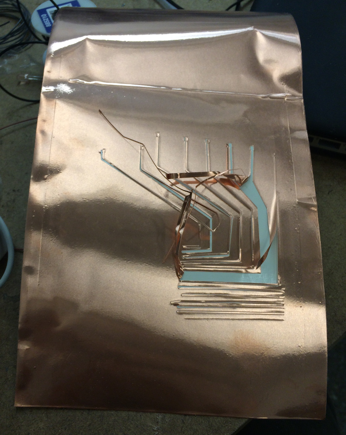
Doesn't that vinyl cut circuit look great? Or alternatively, where I learned that the vinyl cutter isn't a magical tool that can make any circuit. This picture highlights two problems I ran into: 1. The adhesive for the copper tape isn't very strong, meaning it is very common for the traces to peel up when making thin circuits. 2. I planned to use the full range of the copper tape (6"), but the vinyl cutter can only cut the inner 4.7". I didn't plan for this in my design, and this really was the deathknell of my project, as once the foam was milled I was more or less locked into using the copper sheets I had designed.
But, I didn't notice that the vinyl cutter couldn't cut the full 6 inches and my project was fundamentally doomed for multiple hours (really a whole day), and spent all that time troubleshooting how to solve problem #1 so that the I could make a functioning circuit that didn't peel up immediately. By flipping the logic of the circuit, such that the current carrying traces were the widest traces and the small peelable traces were just the separaters between the traces, then after a lot of manual work routing traces in Inkscape, and a redesign of the PCA8695 board in Eagle ("the spider" - shown below), that approach did work and I had a vinyl cut large format circuit! I noticed that the vinyl tended to peel up at sharp corners, so thats one reason why I made the curvy wackadoodle trace. The other reason is it looks nice. At the point I took the picture, the realization that the vinyl cutter wouldn't cut to the 6-inch width of the copper tape became apparent. Also at this point, one of my classmates announced that there were no more 0.01" endmills, which is when I threw in the towel on my project and decided to start writing this beautiful documentation.
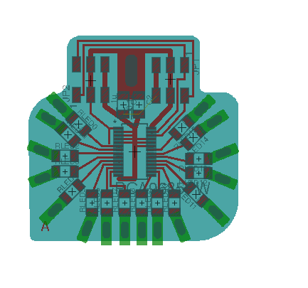
PCA8695 LED driver board revision 2
If you made it this far, I suppose I can try to give you my takeaway about working on this project. Overall, even though the project is incomplete, I'm pretty happy with what I accomplished. I ran into a lot of issues, spent a damn lot of time trying to fix them, and in a few cases actually managed to solve them. Coming from a non-fabrication background, that is pretty satisfying. In fact, if all the fabrication steps went really well and I was instead hung up on writing the software to run the thing, I don't think I would have found it nearly as educational. Struggling with the processes, busting my chops with the modeling, trying new tools, overall was a pretty productive week for getting a survey of the course over again. Besides, If I actually wanted a functioning piece, I would have bought all the premade LED matrixes and whatnot...