
This week, I milled my PCB board and stuffed it (soldered the resistors, capacitors, etc. onto the board). The board on the CBA MIT website is hello.D11C.serial.5V.1.1 (located on this website: http://academy.cba.mit.edu/classes/embedded_programming/index.html)
The milling process was much harder than I thought - I messed up so many times before I got it to come out right! 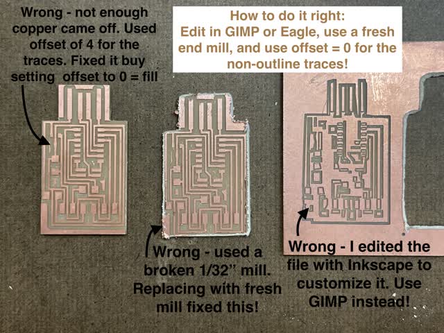 So, here are my tips and tricks to future students for how to get it right:
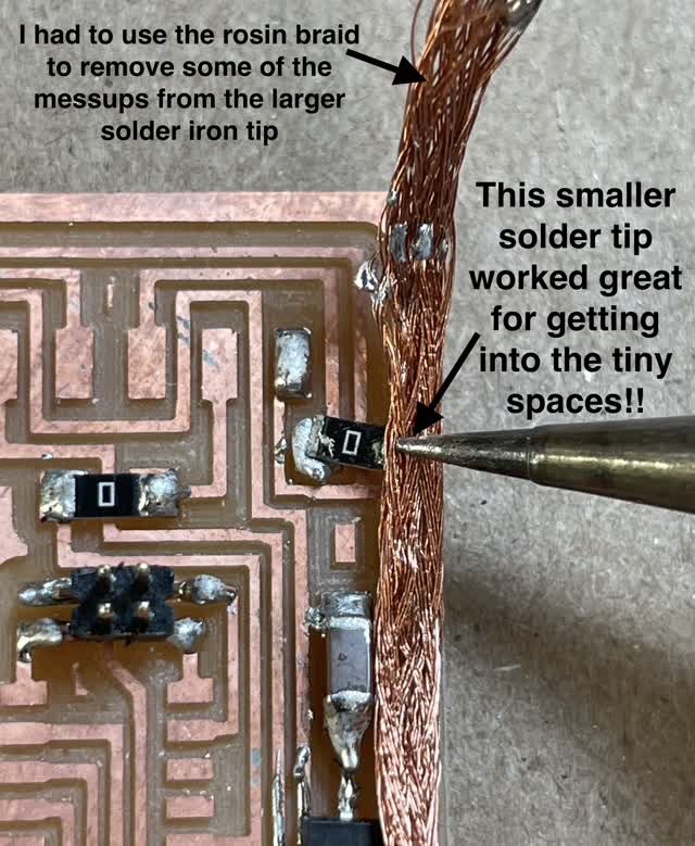
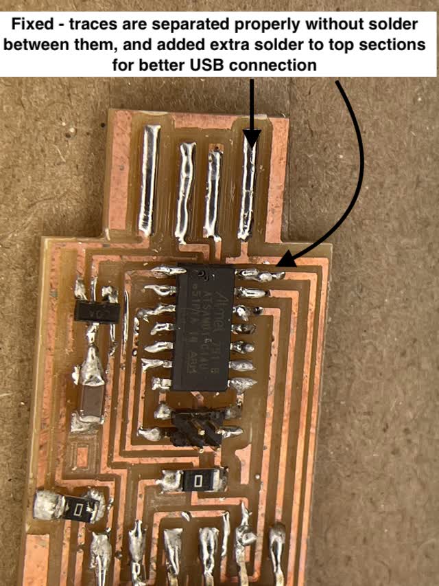
For the soldering process, I didn't have too much trouble since I had soldered before. However, I did run into a few difficulties.
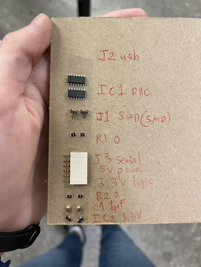
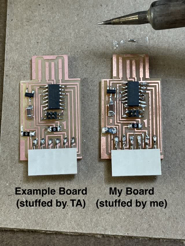
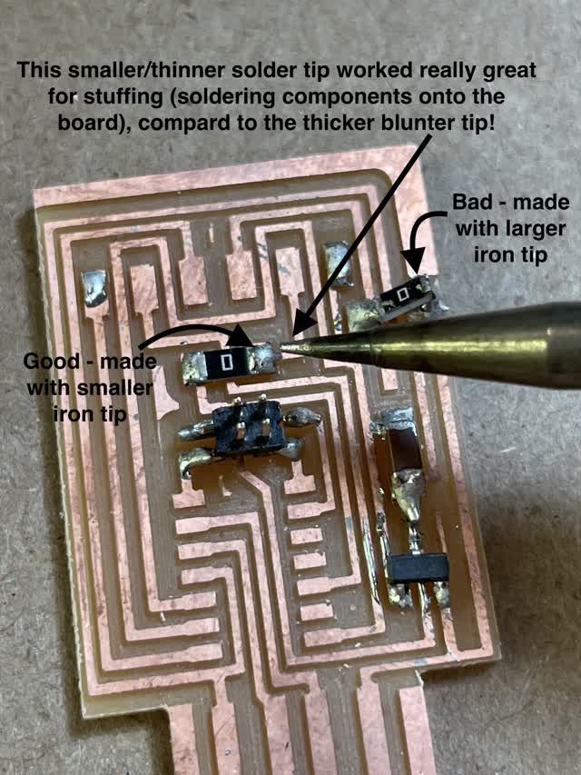
Above is an image of the different components that I stuffed onto the board (LEFT), and an image of my final stuffed board (RIGHT).
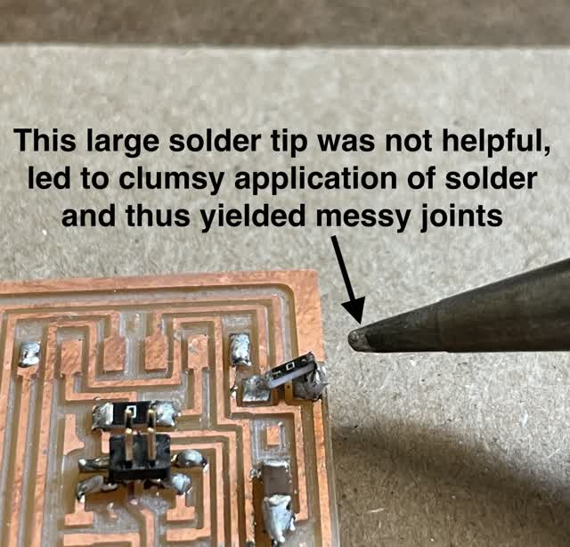
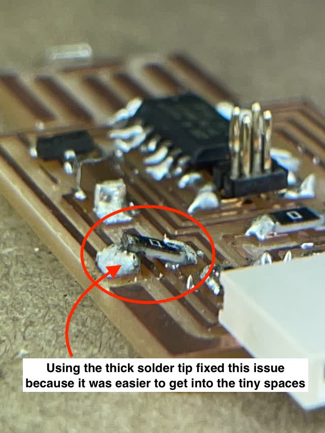
Here were some of my mess-ups (including using the wrong solder iron tip which was too big and clumsy):
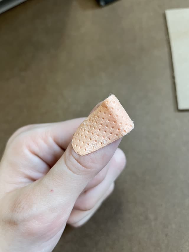
Unfortunately, while trying to take a video of myself soldering, I accidentally bumped my fingeragainstthe solderiron tip while it was hot. Since 65 degrees Celcius was required to properly melt the solder, with 1 second of exposure at that temperature I got a 1st or 2nd degree burn. Tip to future students: even though the example videos show usage of the solder iron without gloves, you may want to consider getting heat-protective gloves (there are apparently some that are quite recommended for workers to wear while soldering!)

Group Project:
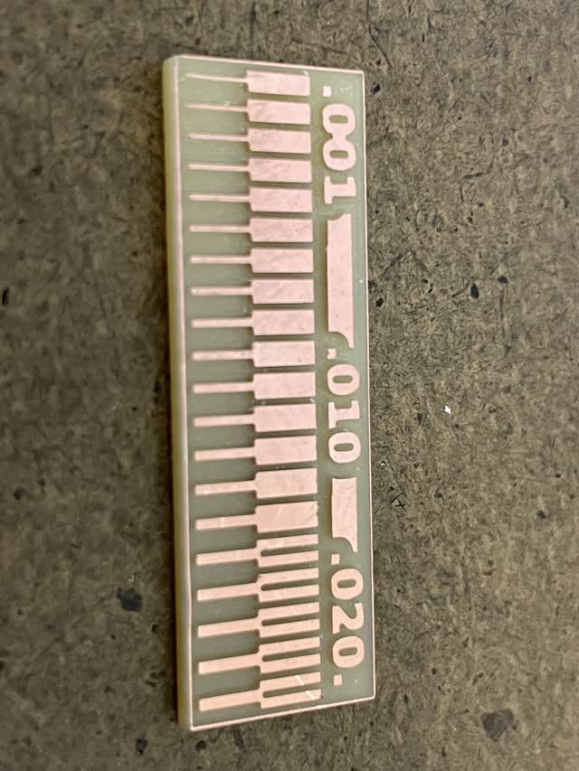
We milled a template of differently sized traces onto a board, to see what size trace and what size gaps wold be best for design parameters.
From this photo below, we can see that the very tiny traces don't end up particularly large enough to solder onto. The optimal trace width is about 0.3 mm, and the optimal distance between the tracesis about 0.4mm. On the image below, 0.0118 inch is optimal for the traces and 0.157 inch is optimal for spacing between the traces.
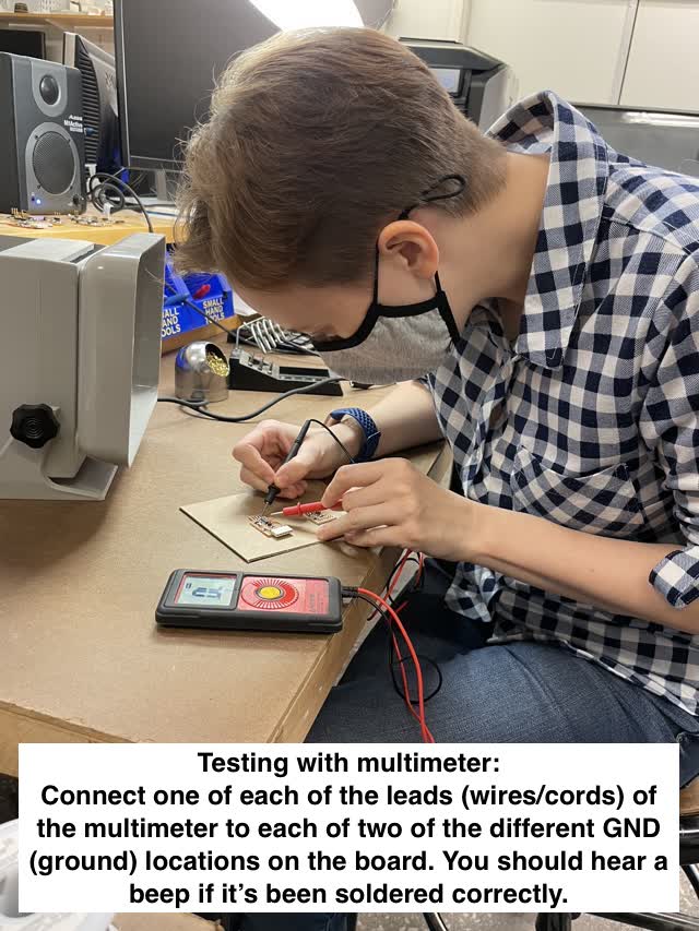
Lastly, I tested my PCB board with a multimeter. I connected the black and red connectors to different GND (ground) locations on the board and if it beeped, there was a connection.


Additional Notes / Modela Instructions
https://www.mokotechnology.com/pcb-milling-board/
How To Mill The Traces:
1) Use hex to insert & tighten a 1/64" end mill into the equipment.
2) Open terminal, and click on mods on the desktop. Select programs > Open Server Program > Roland > Mill > SRM-20 > PCB png (SRM-20 PCB png)
3) Load your file into mods (Select PNG File button), make sure dimensions are right (see photo). Change DPI if needed. (e.g. to 2000 DPI in mods interface for the Roland mill, if I exported PNG with 1000 DPI from Eagle when making my own PCB design)
4) Click on Mill Traces under Set PCB Defaults section within mods
5) Origin: Under Roland SRM-20 Milling Machine section in mods, set values and click Move to Origin to move the mill to a specific spot in the lower left corner of your part
The lower left of your image in mods is the origin. In the equipment, y axis is into the machine and x axis is along the width of the machine.
6) Use Hex Key to looser and bring down the 1/64" end mill to touch the surface
7) Record your origin values on a piece of paper
8) Set offset numer (offset = 0, where 0 = fill)
9) Click Calculate
10) Click on the "Send File to Device" button
How To Mill The Outline:
Same as above, except:
What is Offset?
offset 1 = less material taken off
offset 4 = takes more off
offset fill = takes it all off.
Which end mills should I use for milling the outline versus the interior traces?
Do outline / cutout of the edge of the board with 1/32" end mill
Do the exterior (main design) with 1/64" end mill
Add PNG
Set origin
Unscrew end mill with hex and make it go down.
Move to origin
Mill outline
Calculate
Send to device
Click "Mill Outline" instead of "Mill Traces" when doing the outline, & use 1/32" mill for the outline/outer cutout
If it blinks, turn it off and on again
To scale, load PNG and view the bottom dimensions in mods, e.g. 0.906" x 1.520" for this board template they gave us
ERRORI I MADE:
I did not tighten the hex tight enough! (mill was loose)
Offset 4
Set offset number to (0=fill) will make sure all the copper comes off :)
Oopsie - I loaded my file and it didn't work. Needed to invert it at least possibly ??
Oopsie 2 - Used a broken mill fort he outline and it was super jagged and thick cutout line
It gave jagged outline
we used fill = 0 this time and then tried again, and with a new fresh mill from the TA.
created with
Website Builder Software .