This week we learned how to operate a PCB mill in order to manufacture a PCB from an existing board design file. The exemplary circuit I chose to mill was Neil's programmer board featuring a SAMD11C microcontroller. More details and explanations on what a programmer board is and how it is used can be found in Week 6 - Embedded Programming. The traces for this board can be found as a PNG in Neil's class material under the name USB-D11C-SWD-10 pin here.
Fundamentals of PCB Design to Mill
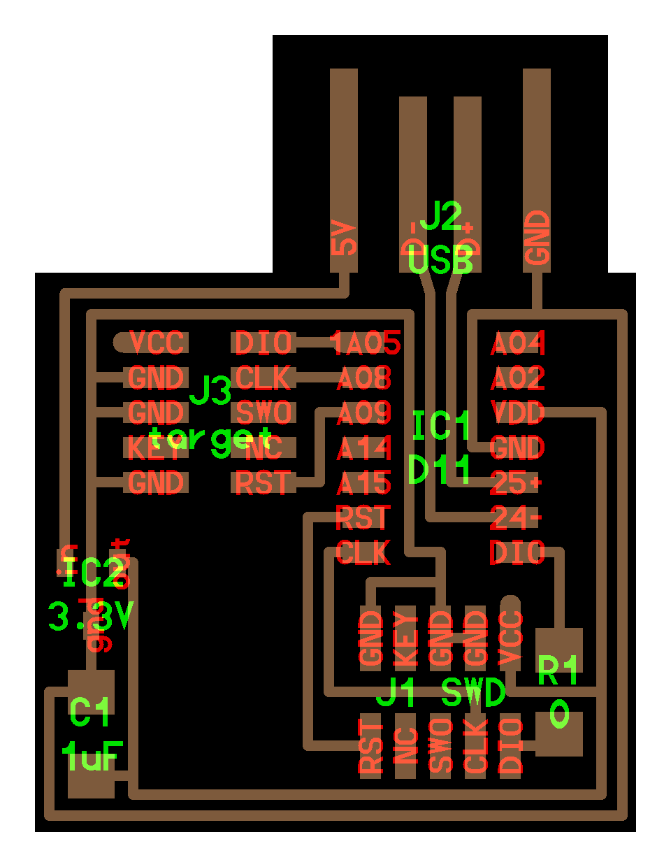
The layout of the PCB that I am going to manufacture this week is shown below, taken from the HTMaA website, as mentioned above.

To briefly introduce into the key features of this board:
- Atmel SAM D11C microcontroller: At the heart of functionality of this board is the SAMD microcontroller. It is a microcontroller using ARM architecture, as opposed to the ATtiny series using AVR architecture. The datasheet for this microcontroller can be found here.
- USB interface: One key advantage of the SAMD microncontrollers is that they can be programmed directly via USB once bootloaded (please refer to Jake's microntroller primer or my documentation on Week 6 - Embedded Programming for reference of what that means). The USB interface features four pads, the outer pads are voltage(5V) and GND used to power the microcontroller (after regulation, see below); the two inner pads are pads for data transfer, thus can be used for programming of the microntroller.
- 3.3V voltage regulator (can be found here): This is a key feature of a PCB featuring a SAM D11 microcontroller, as the USB connection by which this board is powered provides 5V. The microcontroller, however, needs to be operated at 3.3V to not be damaged. This voltage regulator can take inputs between 5v and 30V but can only support currents up to 100mA. For circuits carrying larger currents, a larger voltage regulator needs to be used.
- Voltage-stabilizing capacitor: In close proximity to the voltage regulator it is recommended to place a capacitor in parallel with voltage and ground in order to balance small fluctuations in voltage. This is recommended as a general practice wherever a stable voltage input/ouptut is needed and may comprise multiple capacitors spanning various orders of magnitude in capacitance to allow for both fast reactance with little charge stored as well as slower reactance with large amounts of charge stored to balance large voltage flucuations.
- Contact headers: This board features two 10-pin headers. While one is labeled SWD and the other is labeled SWD, both are SWD interfaces. The contact header in the bottom is used to program the SAM D11 microcontroller on this board via a SWD connection. The pin headers on the left are used analogously to later program other SAMD micrcontrollers using this board via the SWD interface (hence the name programmer board). As mentioned above, details on programmers can be found in the documentation of Week 6 - Embedded Programming.
PCB Milling
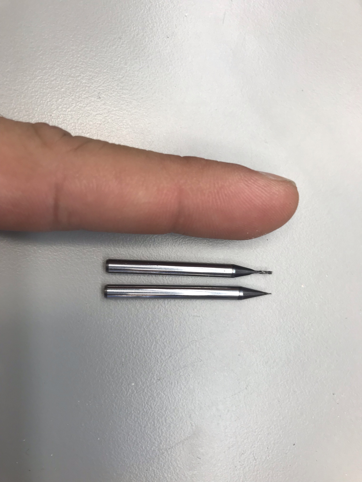
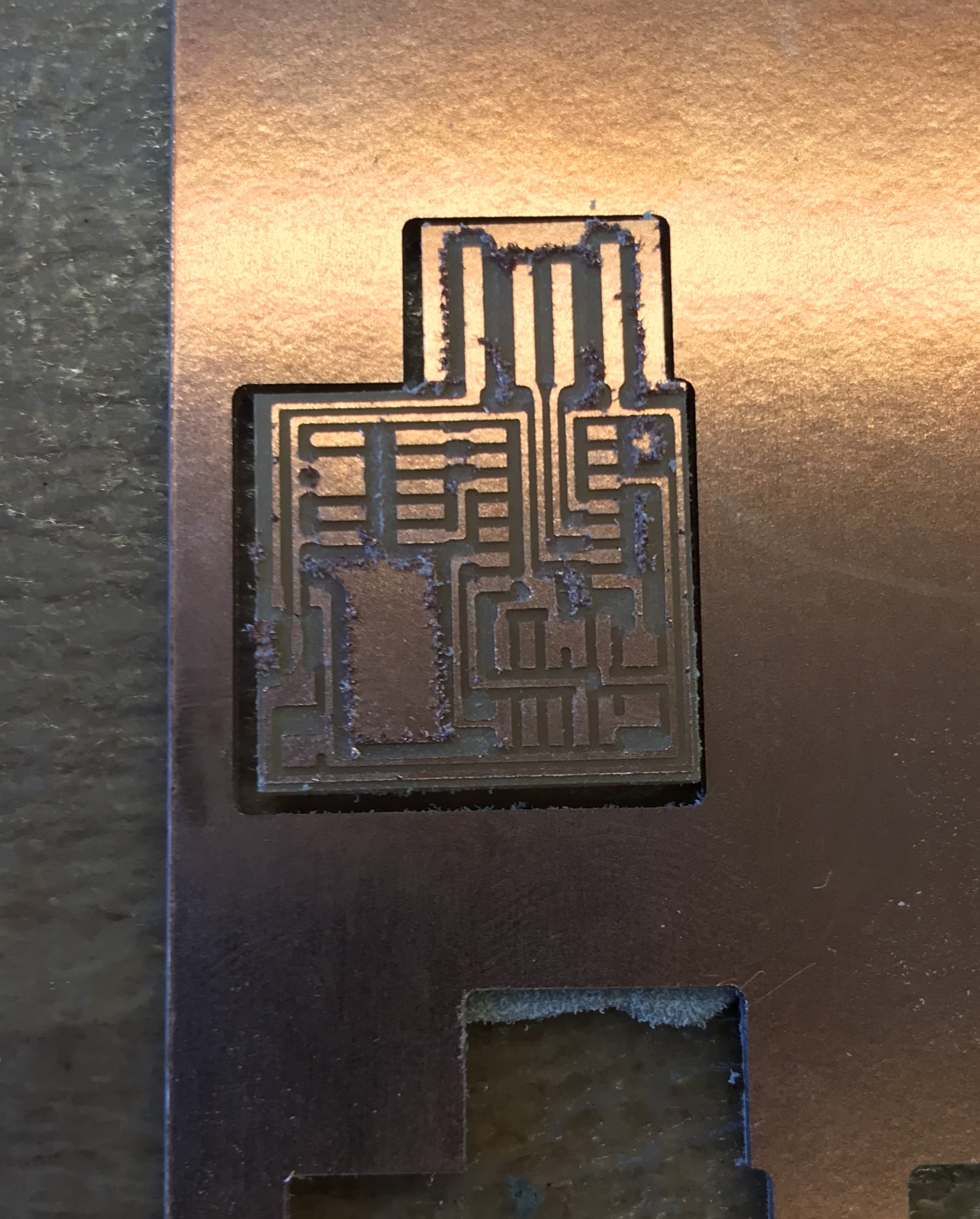
In order to mill the traces contained in the design file shown above, we use a PCB mill. This is in contrast to commercial board houses typically using photolithography processes for PCB manufacturing which, however, require much more specialized equipment and the use of chemicals. For our prototyping purposes we thus use the simpler method of physically milling into FR-1 substrates - 1/8 inch thick phenolic paper with a copper coating on top - at the cost of being limited in trace width and spacing. PCB design files are typically so-called Gerber files (read more on that in Week 4 - Electronics Design), or image files in SVG or PNG format depending on the software used. The PCB mill shown below, the Othermill, used for this week's assignment, can work with both Gerber files (preferred) or image files. In order to mill the traces of this PCB we used two tools: A 1/32" flat end mill for the outline and larger features as well as a 1/64" flat end mill for finer traces and smaller spacings. In a test structure we determined that technically our PCB mill can achieve resolutions down to 10 mil wide traces as well as 15 mil spacings using the latter tool. Practically, I learned later on in the semester that it is wise to not push those limits and adhere to design rules limiting trace width to 14 mils and trace spacings to 17 mils.
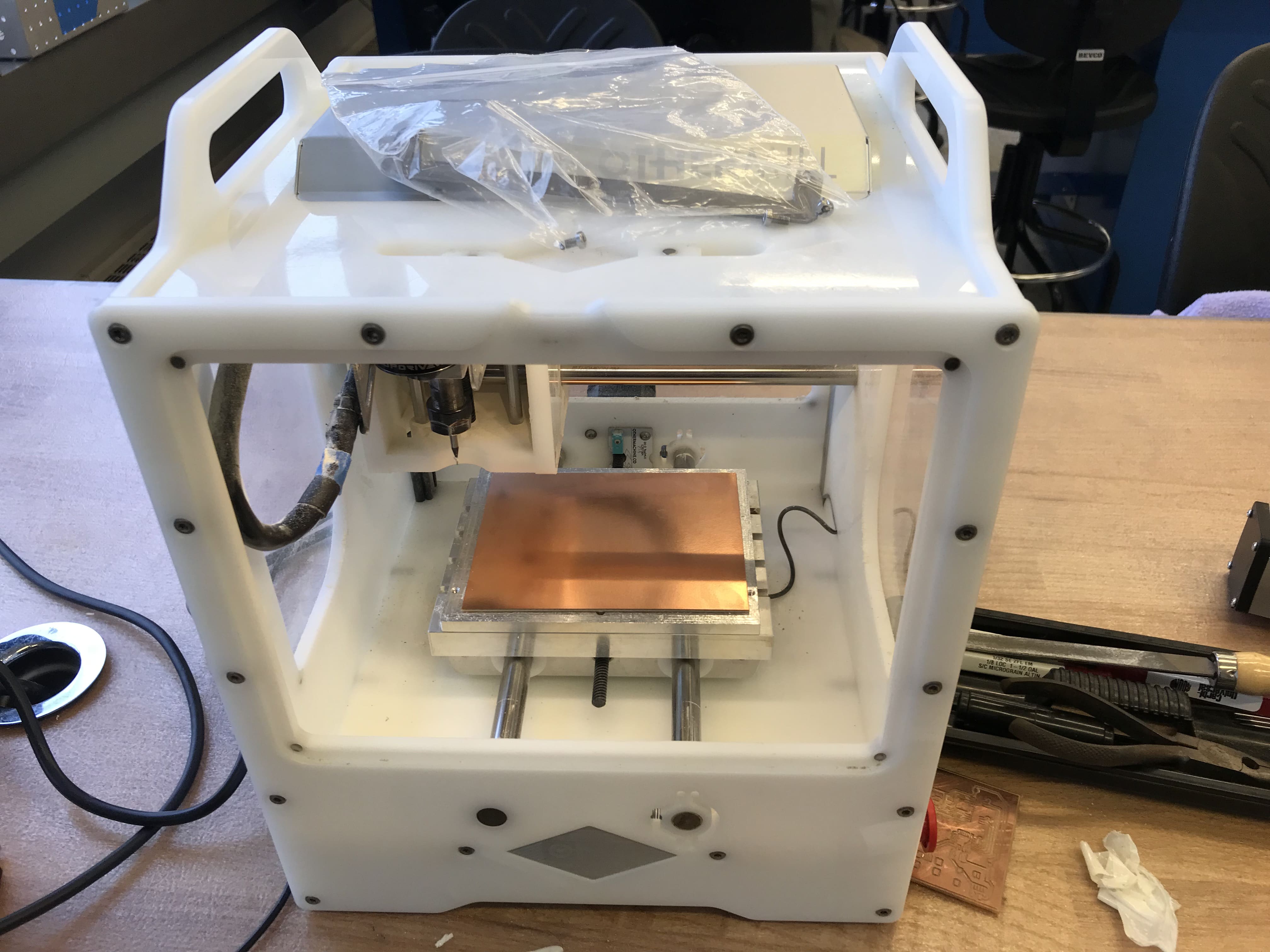
An impression of the milling process and the milled PCB before clean-up is given in the video and image below.
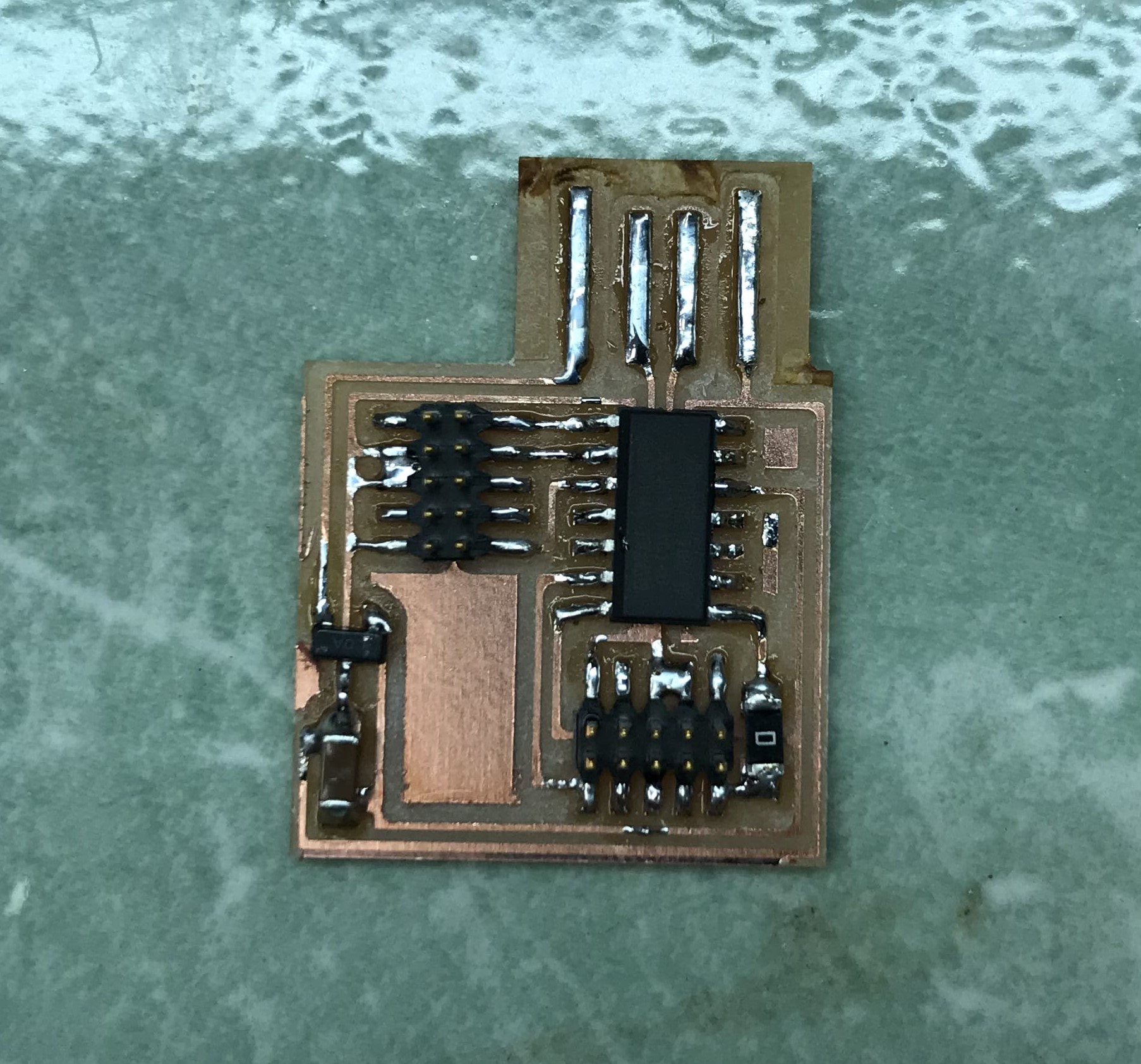
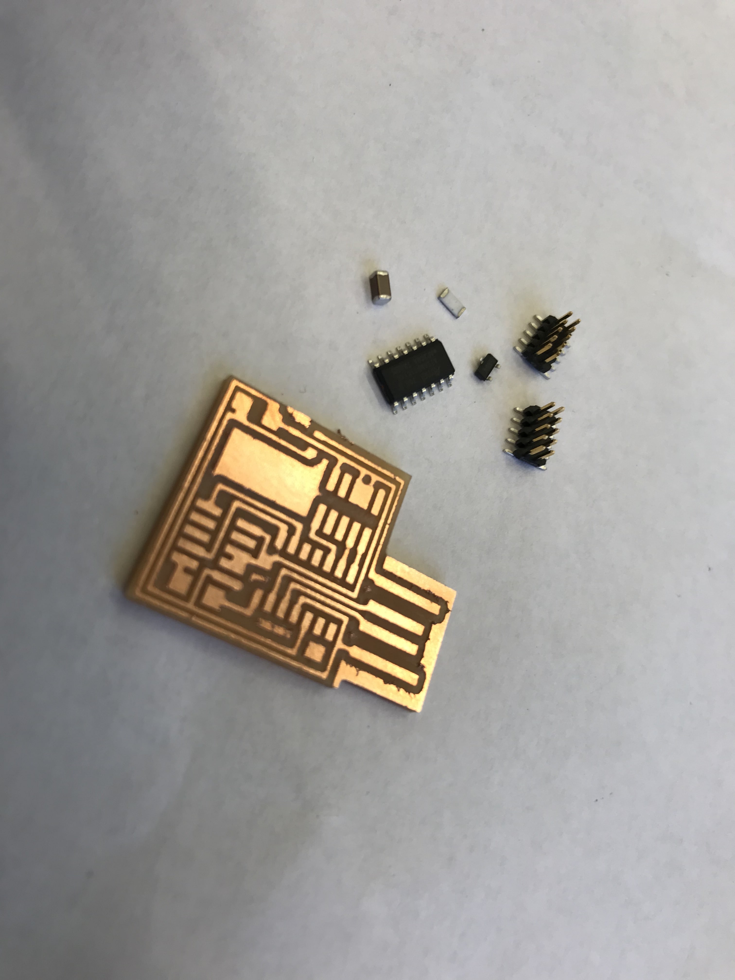
PCB Stuffing
In the last step, the PCB is being stuffed, which is the term used for attaching the electronic components to the board by soldering. The cleaned up PCB with all required components is shown below.
Care must be taken to use a fine enough solder tip. Issues that arose in my case were bending and melting of pin heads as well unwanted connections due to heat exposure using too large of a solder tip.
As a final note, in order to make a stable USB connection, two steps are recommended:
- Heat the FR-1 around the USB contacts and pull off any copper with a tweezer that is not part part of the four USB contact pads.
- Due to insufficient thickness of the PCB substrate it is recommended to either add solder onto the USB contact pads in order to increase thickness or tape a piece of cardboard/business card/multiple layers of vinyl tape to the bottom side of the substrate.