Week 2 - Electronics Production
This weeks individual and group assignment concerned PCB milling, soldering, and design verification. Details on the group assignment, which covered characterization of the PCB mill's capabilities, can be found here.
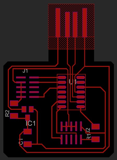
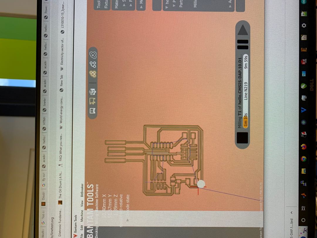
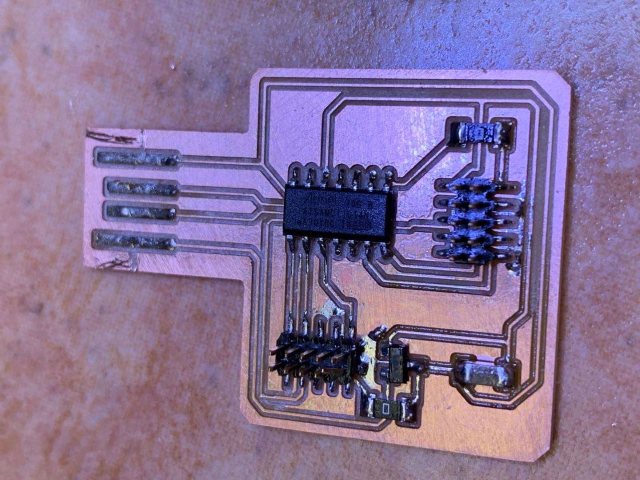
The first part of the individual assignment was to mill the PCB. The EDS lab has two PCB mills, but I worked on the Bantam Tools mill. The software that comes with the Bantam Tools mill really only likes .brd files, though it does also take .svg picture files. The Roland mill that works with mods can take in PNGs, which is a nice feature, however .brd files are a little more forgiving because they can be integrated with desin rule checkers to determine the parts that need to be milled for clearances and also account for the bit size. The layout shown below is for a bootloader and is what was made during this assignment.
The PCB stock is FR-1, which is a layer of copper over phenolic resin. I do have some experience in PCB design and soldering, however, I have only sent my boards out to a board house to be etched on FR-4. The idea of milling PCB boards has never occurred to me and I didn't even know it was possible, but I'm very intrigued especially because milling seems like a great to get a thick layer of copper such that I'm no longer constrained by etching copper thicknesses. This is useful for power boards that must carry large currents.
The .brd file was loaded into the Bantam Tools software and the design was located to a position that hadn't been cut yet on the stock. In order to make the traces, which are quite fine, the 1/64th inch bit was used first. Once this was carefully installed into the mill, the board outline and holes were turned off in the software and I started the operation. While the board was being milled, the software showed the current location of the bit.
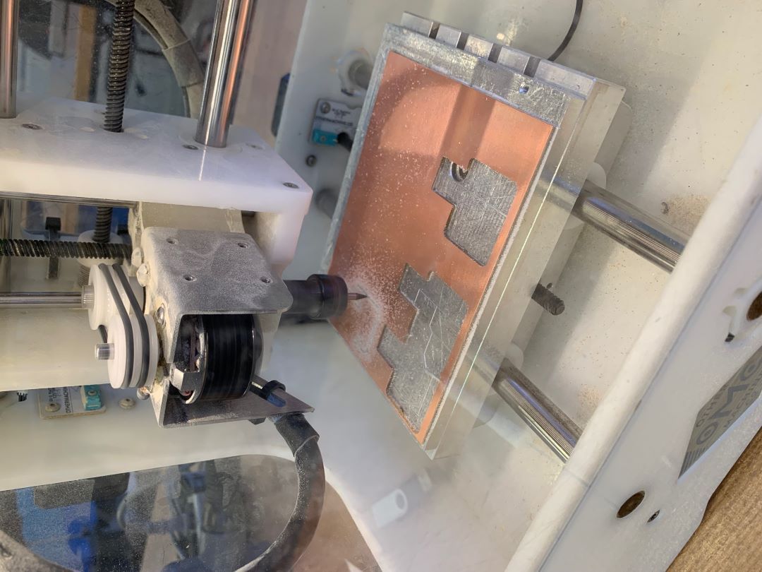
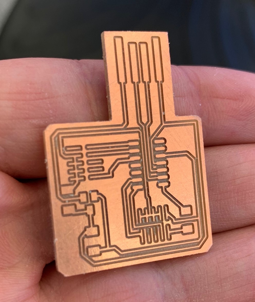
Once the traces were completed, I changed out the bit for a 1/32nd inch bit in order to cut the board outline (which would take much longer on the smaller bit and put unnecessary wear on it). Several pas were needed to cut through the board. When the outline was cut, I used a flathead screw driver to extract it from the bed. I removed the adhesive tape on the back and used a fine grit sandpaper to remove the burs from the surface and from the edges. The blank board is shown below.
When it came to stuffing the board, I have a slight leg up over some others in the class as I've soldered extensively in the past. However, I typically work with through-hole components due to the high current nature of my projects, so I don't have too much experience with surface mount soldering. The microscopes, tweezers, fine pointed soldering iron tips, flux rosin pen, and thin solder wire were all great help in the process of soldering such small components one such small traces. The task was exacerbated in this version of the bootloader in which the copper plane was not milled out. This means that the solder can easily jump the gap onto the copper plane. While the copper plane is not connected to any potential, it may be capacitively coupled and, additionally, if there are two points where the solder jumps the gap onto the plane, those two points are now at the same potential. All this to say I was very careful. I started with the smallest components, the zero Ohm resistors, the capacitor, and the voltage regulator. I first used the flux pen to deoxidize the pads I'm about to solder to. Then with the microscope and tweezers, I carefully placed the component in the correct position. The first joint is the hardest, because you don't want to knock the component off the pad. So I first carefully place the soldering iron tip on the pad close to, but not touch the component. After a a second or two, I add solder and the joint is complete. The next pad is easier because now the component is anchored down. After the small components, I soldered the IC microcontroller and then the pin headers. If at any point I had two joints combine, I went in with the soldering wick and removed some of the solder. The result turned out pretty good.
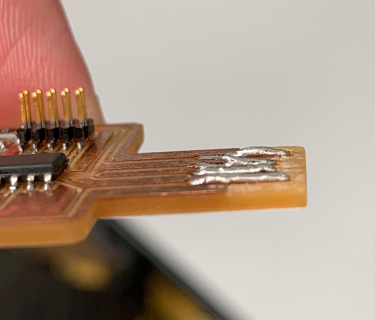
Before I tested it, I needed to tin the USB leads to prevent oxidation, wear and tear, and also add some thickness for clean contact with my computer. I also added a vinyl backing to the back of the USB portion to add to the thickness.
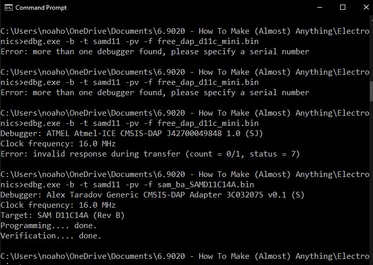
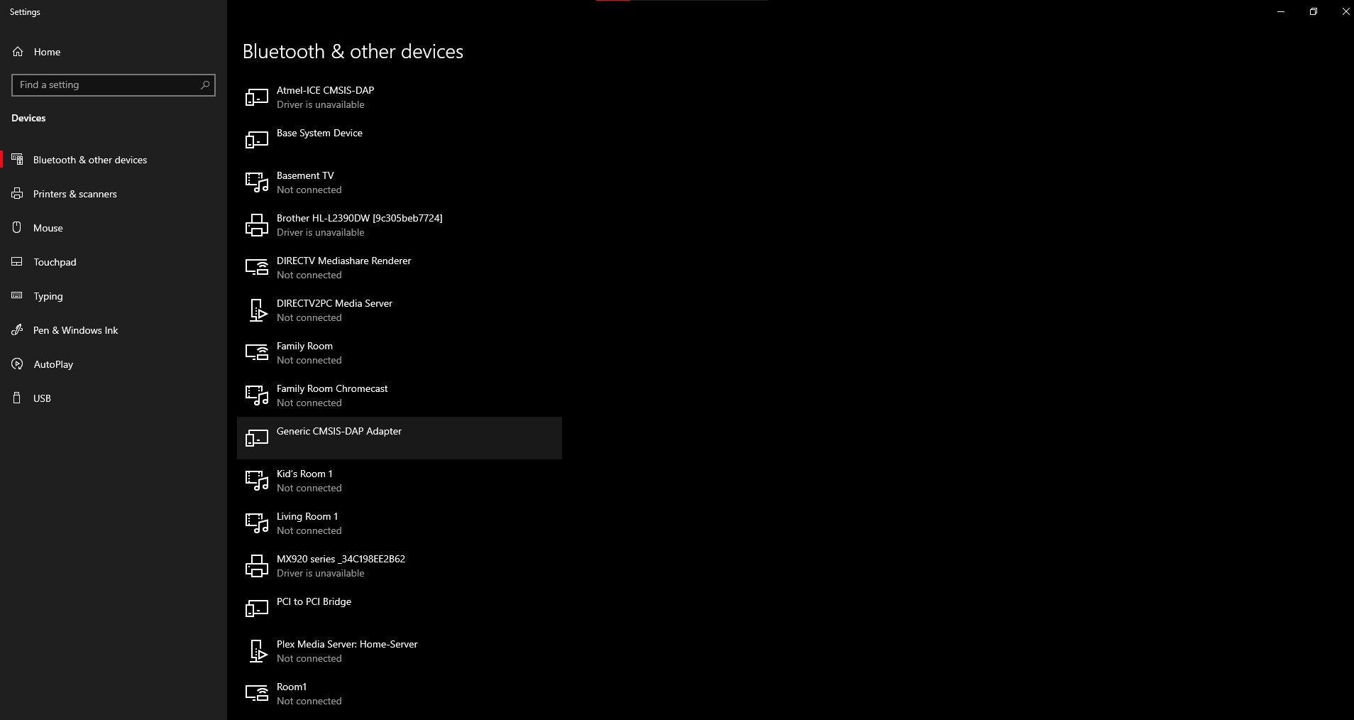
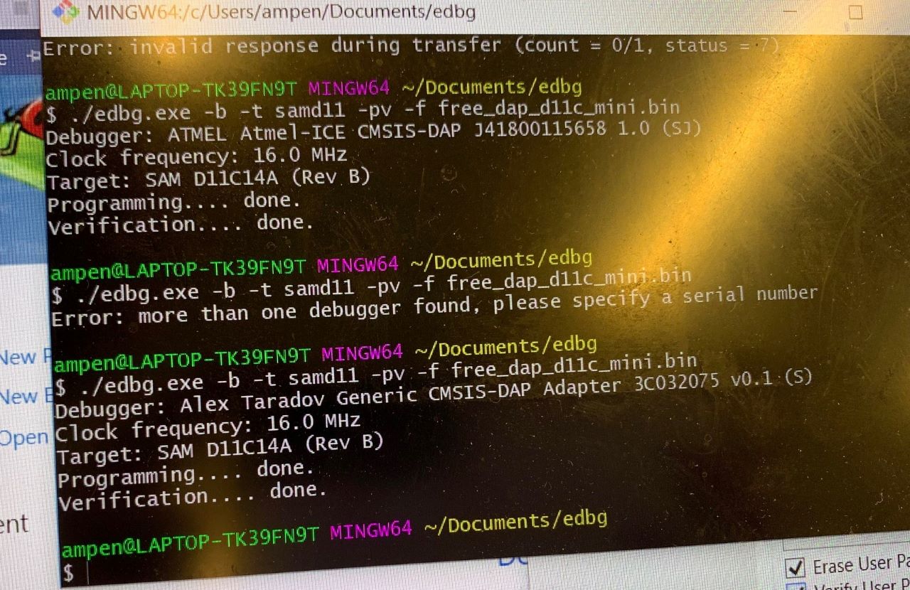
I then plugged the pin header into the programmer and powered the board with a USB. I loaded the EDBG command to program the board and was successful after a few failed attempts due to the board not being thick enough and not making good contact (this was before the tinned USB leads and vinyl backing).
The board then showed up in my devices list.
I was also able to program another board that was erased as a test to make sure my board was correctly programmed. It was successful! No resoldering needed.
Design files for this week can be found here.