Electronics Production
Group Assignment
1. I worked with my group to learn how to mill a PCB board and solder.
Under the guidance of Shop Manager and Technical Instructor Jen O'Brien, I, along with a group of students in the Architecture section learned how to mill a PCB board (Fig. 1A). Jen walked us through all of the steps including launching the program on the computer, setting up the machine, using the vacuum to clean up, and so on. I learned a lot!

Fig. 1A. Learning how to use the PCB milling machine.
As a group, we selected a test board to upload to the machine and mill (Fig. 1B). When the board was finished, we analyzed the pattern giving us an idea of the tolerances of the machine. We notices that some of the very fine lines of copper peeled right off of the plastic layer underneath, meaning we have to design our PCBs appropriately to avoid this (i.e. using route thickness of at least 0.4 mm)

Fig. 1B. Test PCB.
Lastly, Jen taught us how to solder. This included an important lesson on keeping the Architecture shop neat, for example, only removing one drawer at a time to select a component and then putting the drawer back (Fig. 1C). After Jen collected all of the components she needed, she showed us how to secure them to a spare peice of cardboard, how to position the magnifying glass and light over the board, and use the soldering iron and solder to affix the components to the board.
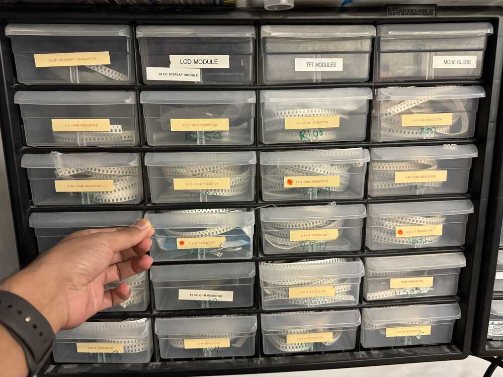
Fig. 1C. Important rule to keep organized.
There was a lot to learn this week, so I was excited to apply it all in the Individual Assignment!
Individual Assignment
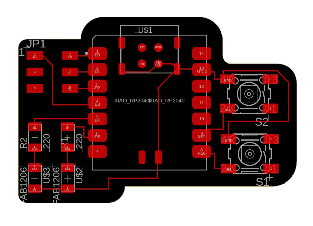
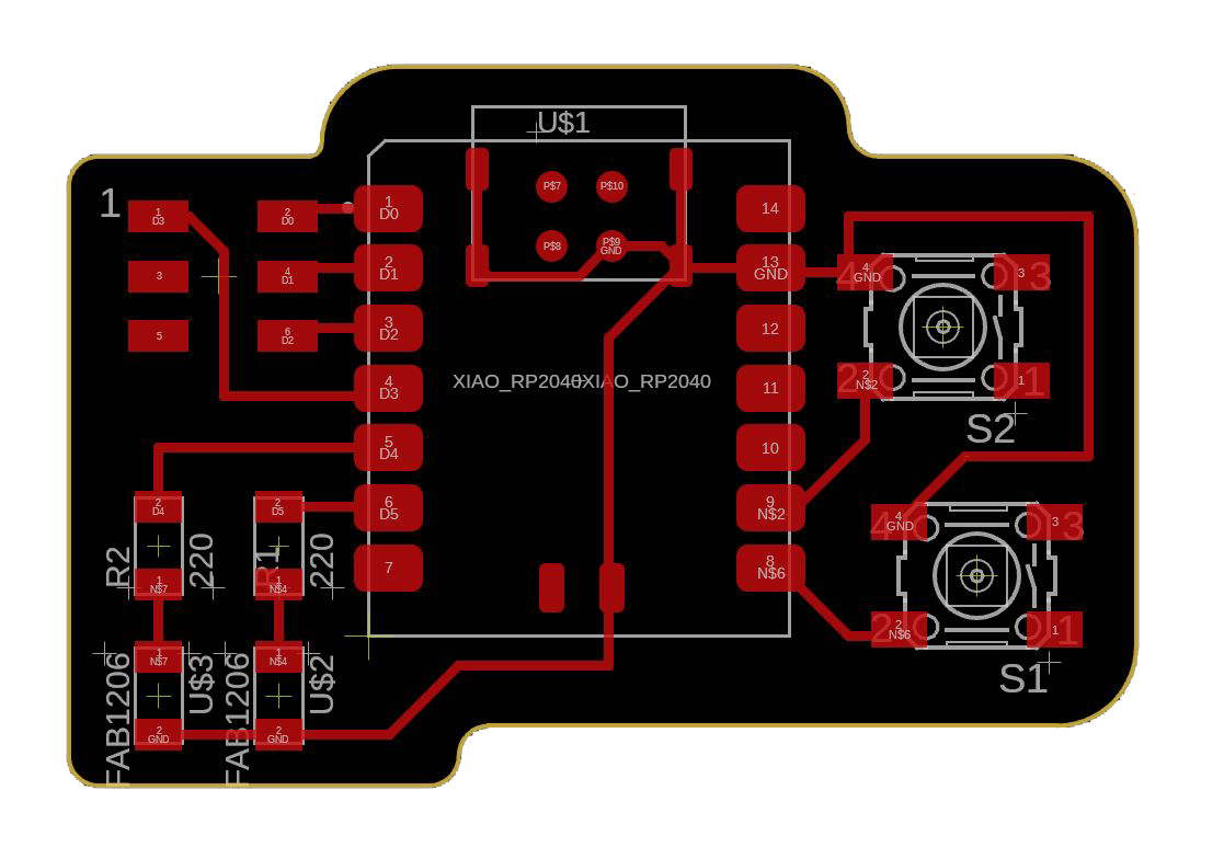
This week, I revisited the previous design from last week and iterated. Originally, the routes were set as 4mil, which I realized was too thin for the milling process.
I changed the line thickness to 16 mil (0.4mm).
Additionally, I made sure the lines are spaced out better and that all the corners of the board are filleted to be smooth when they are grabbed.
The PCB board milling in progress. Important note is to hold the end mill to keep touching the surface of the board when tightening up after setting it to the origin.
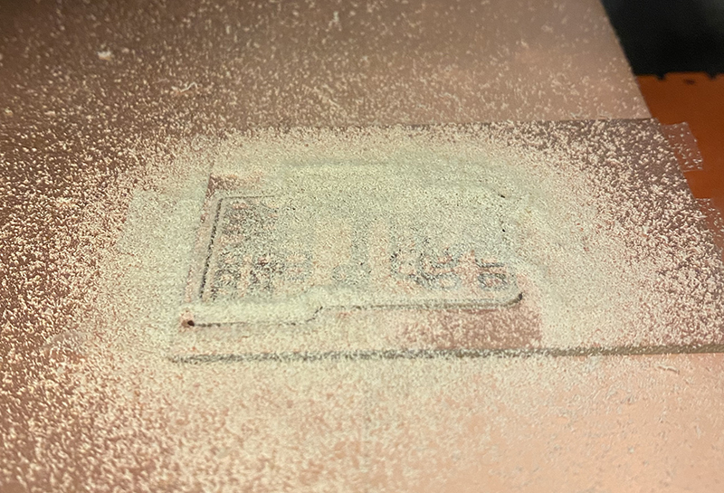
This is how the PCB board initially looks after cutting. As instructed, I used 1/64 for etching, and 1/32 for cutting the boundary.
Dont forget to vacuum before switching to 1/32 end mill, and before taking the board out!
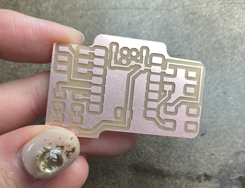
As Jen recommended during the training session this week, I gently rubbed the surface of the board with gojo orange hand soap, and rinsed it with water to remove any potential greasy residue.
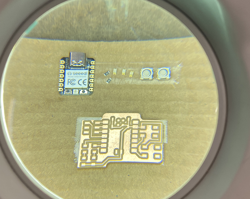
Then I looked through the inventory to find the components I need for soldering which were 2 LEDs, 2 button switches, 2 1k resisters, and a 2x3 connector.
The image above if the view of my soldering setup through the magnifying glass.

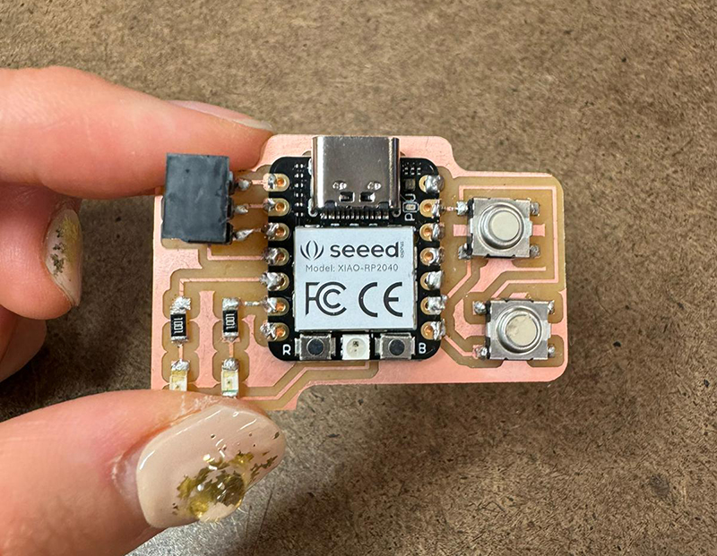
This is how it looks after soldering all the components. I am pretty used to soldering, but soldering super tiny components was challenging because it required better control of hands to apply the appropriate amount of solder.
                  const int Power = 11;
                  const int button1Pin = D8;
                  const int button2Pin = D7;
                  const int led1Pin = D4;
                  const int led2Pin = D5;

                  int led1State = LOW;
                  int led2State = LOW;
                  int button1State = LOW;
                  int button2State = LOW;

                  void setup() {
                    pinMode(button1Pin, INPUT);
                    pinMode(button2Pin, INPUT);
                    pinMode(led1Pin, OUTPUT);
                    pinMode(led2Pin, OUTPUT);
                  }

                  void loop() {
                    button1State = digitalRead(button1Pin);
                    button2State = digitalRead(button2Pin);
                    if (button1State == LOW) {
                      if (button2State == LOW) {
                          digitalWrite (led1Pin, led1State);
                          digitalWrite (led2Pin, led2State);
                        }
                        else {
                          digitalWrite (led1Pin, HIGH);
                          digitalWrite (led2Pin, HIGH);
                        }
                      }
                      else {
                        digitalWrite (led1Pin, LOW);
                        digitalWrite (led2Pin, HIGH);
                      }
                    }
Test code for the buttons and LEDs
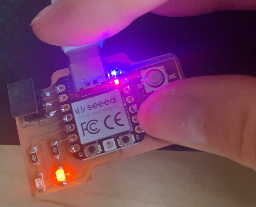
This is the simple blink test with a button after I have uploaded a test code to the board.