HTMAA 2024 - Week 5
Electronics Design
HomeThis week we learned about electronics design, and even though I'd heard from so many people to start with KiCad, I spent a LOT, A LOT, A LOT, A LOTTT of time looking for an electronics simulator that fit what I was looking for.
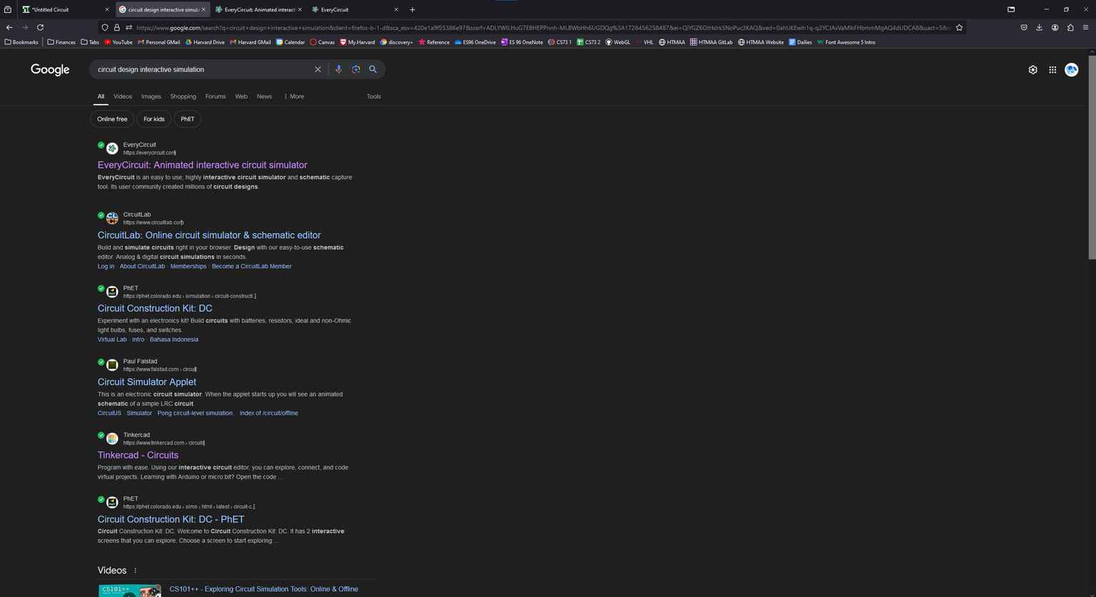
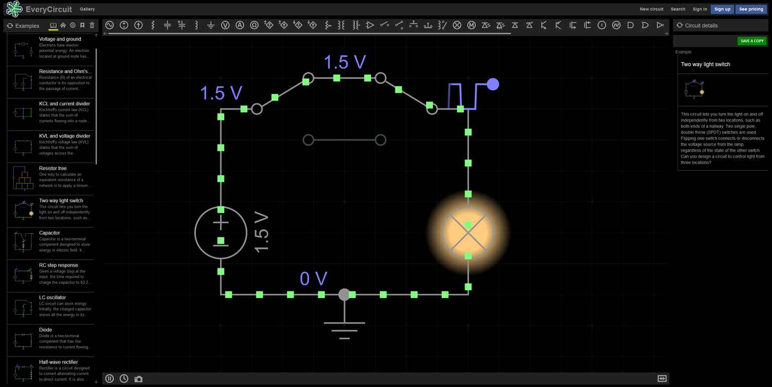


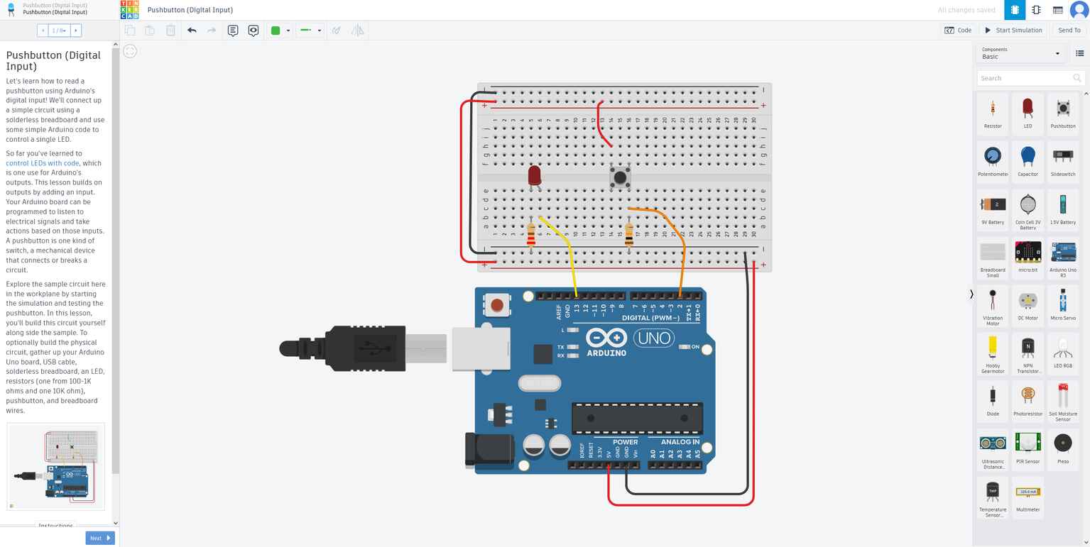
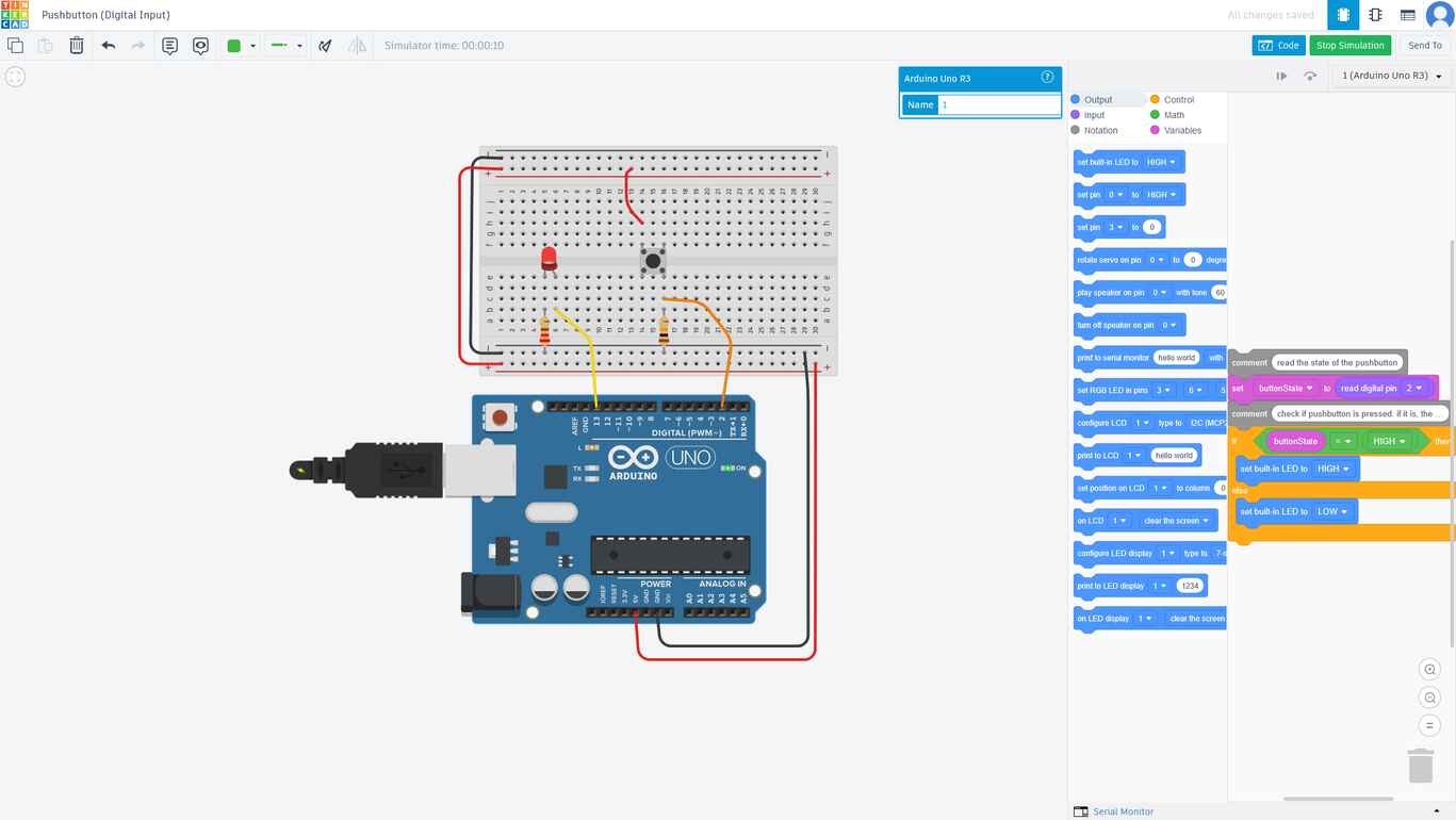
I knew what I was looking for: a REAL TIME INTERACTIVE electronics simulator, like Multisim, a software I used in high school for my digital electronics class.
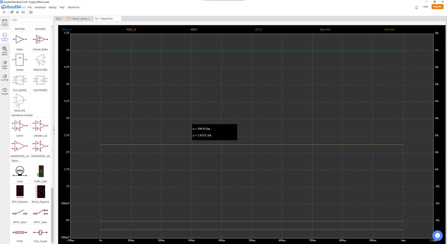
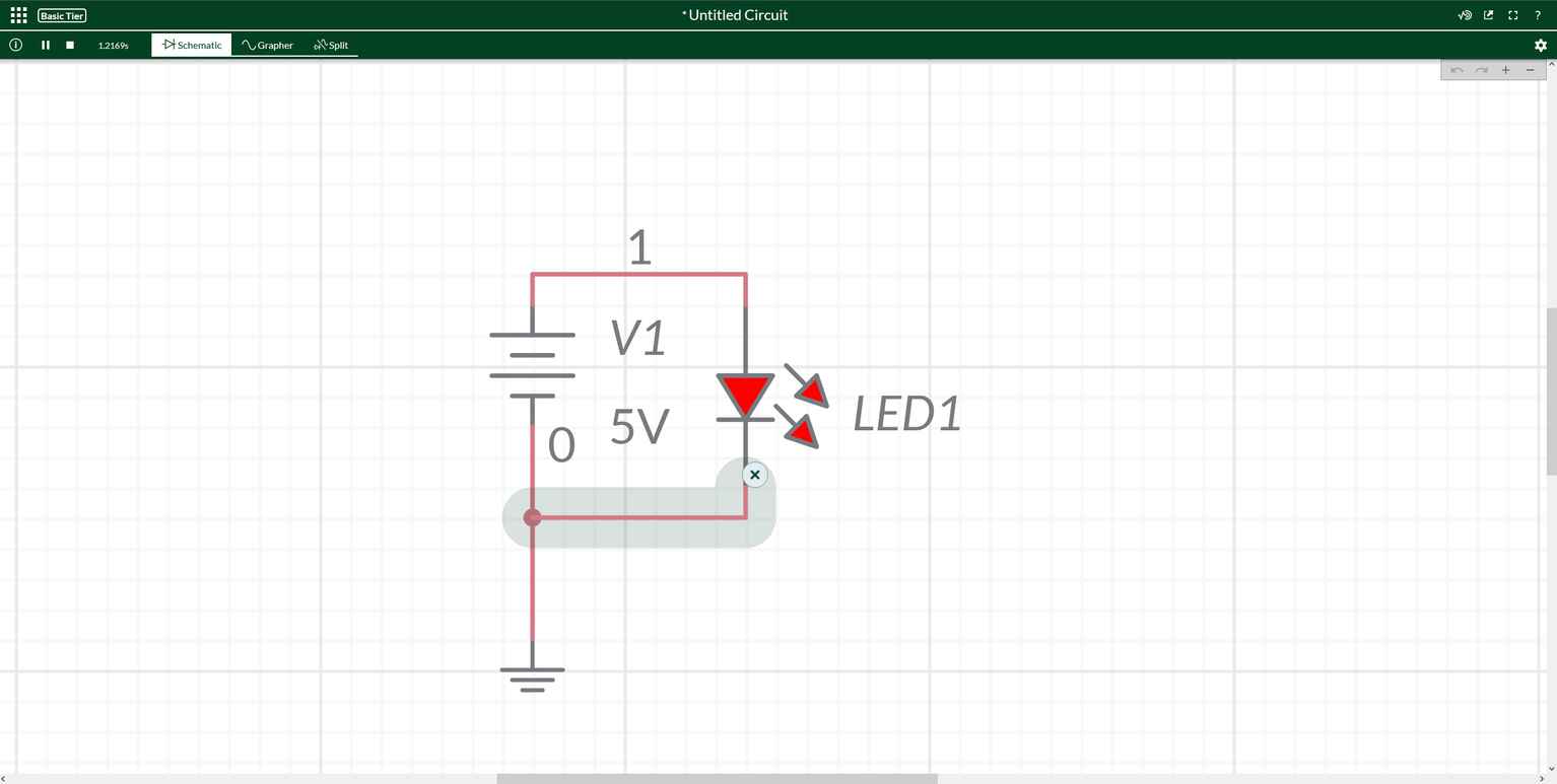
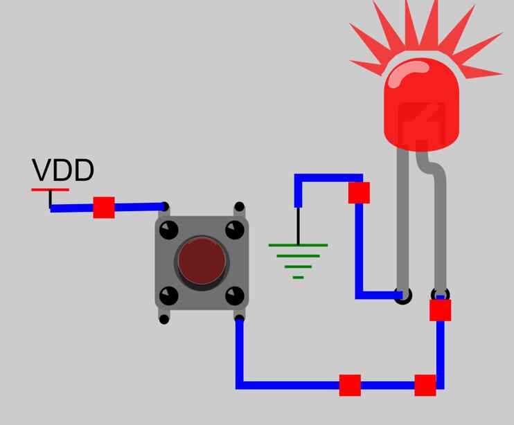
Unlike other SPICE software, you could place interactive components like switches to see how inputs and outputs change in real time based on your input for combinational logic. Check out this demonstration of that functionality.
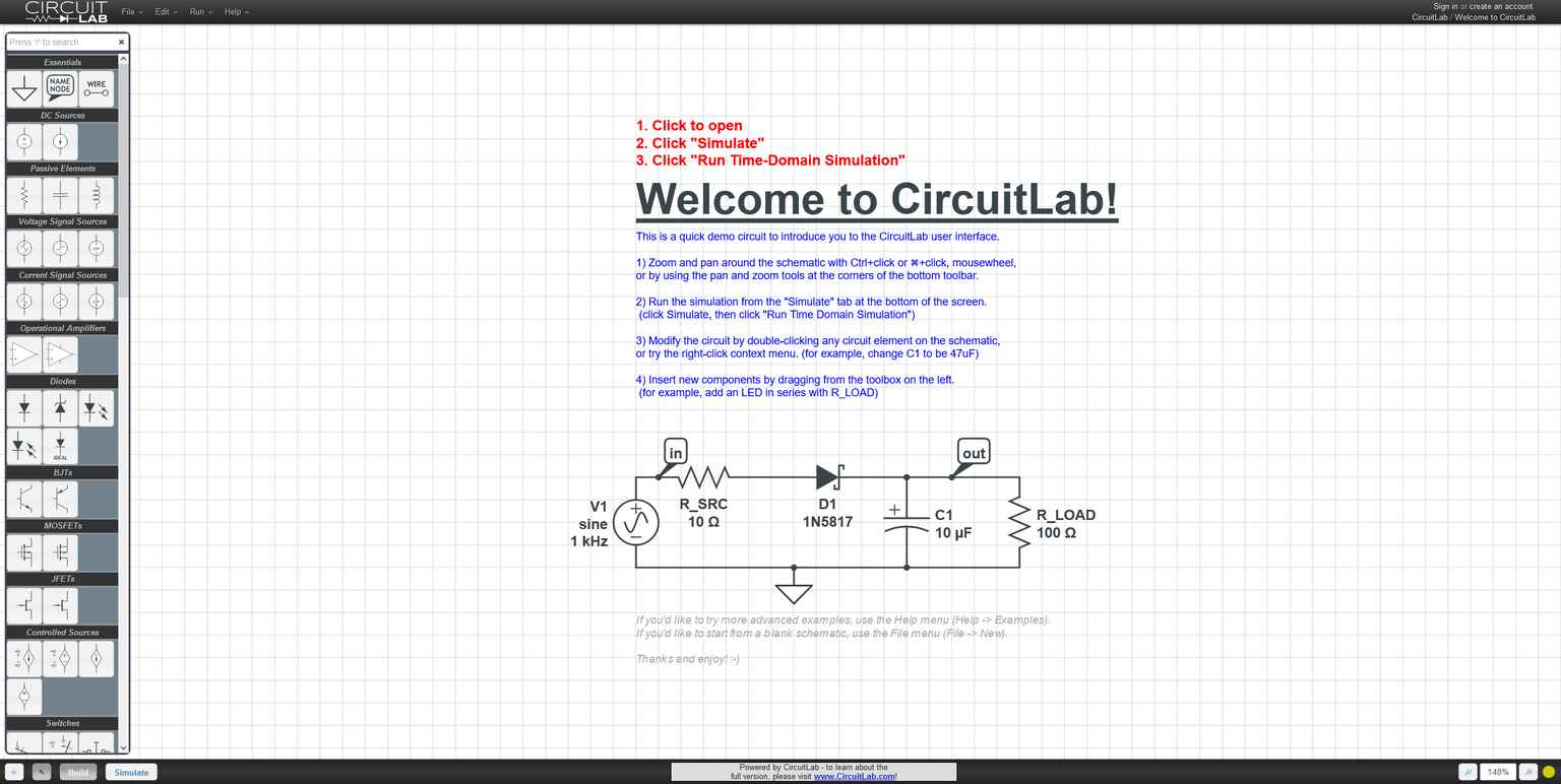
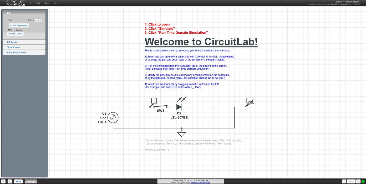
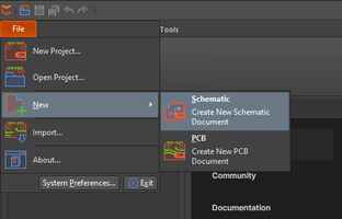
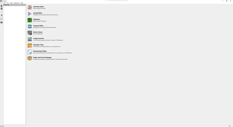
Couldn't find one like that. So I went back to the one that everyone was using— KiCad.
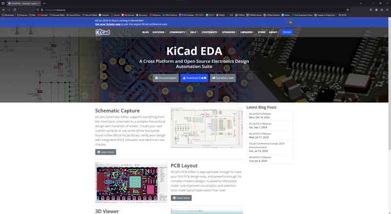
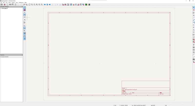
I downloaded it and opened a new file.
Pretty standard, looked like the other SPICE softwares I saw before. I decided to follow this guide to get started.
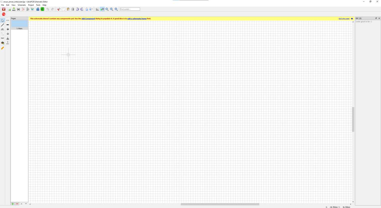
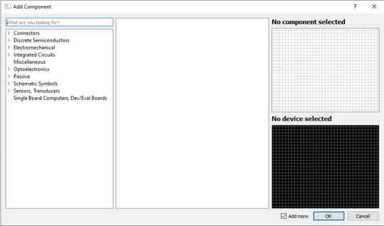
I tried placing a few components using the components menu.
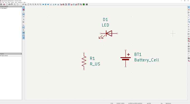
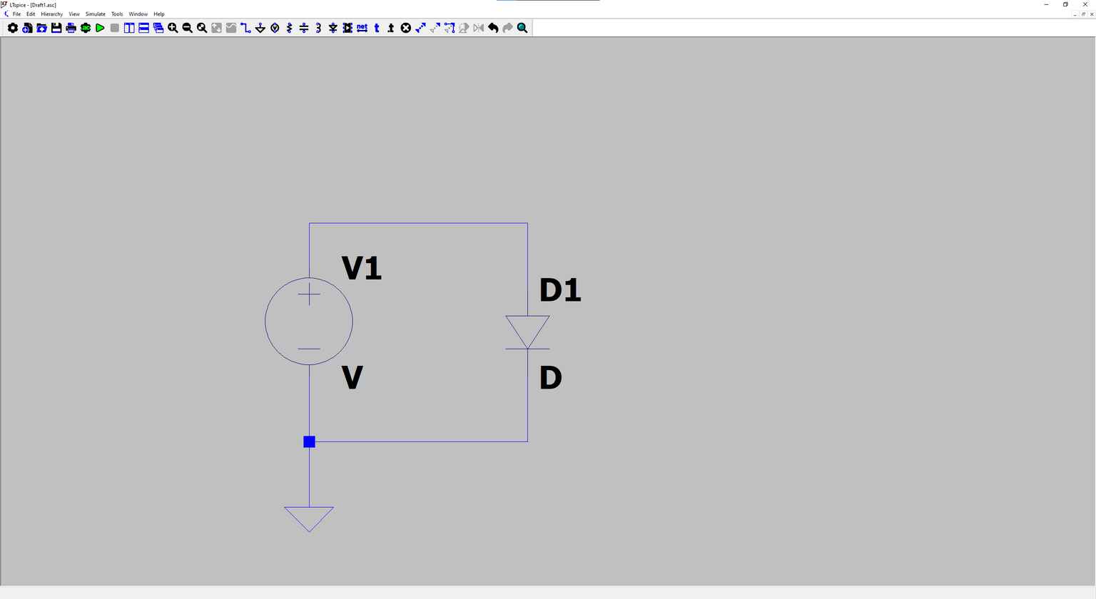
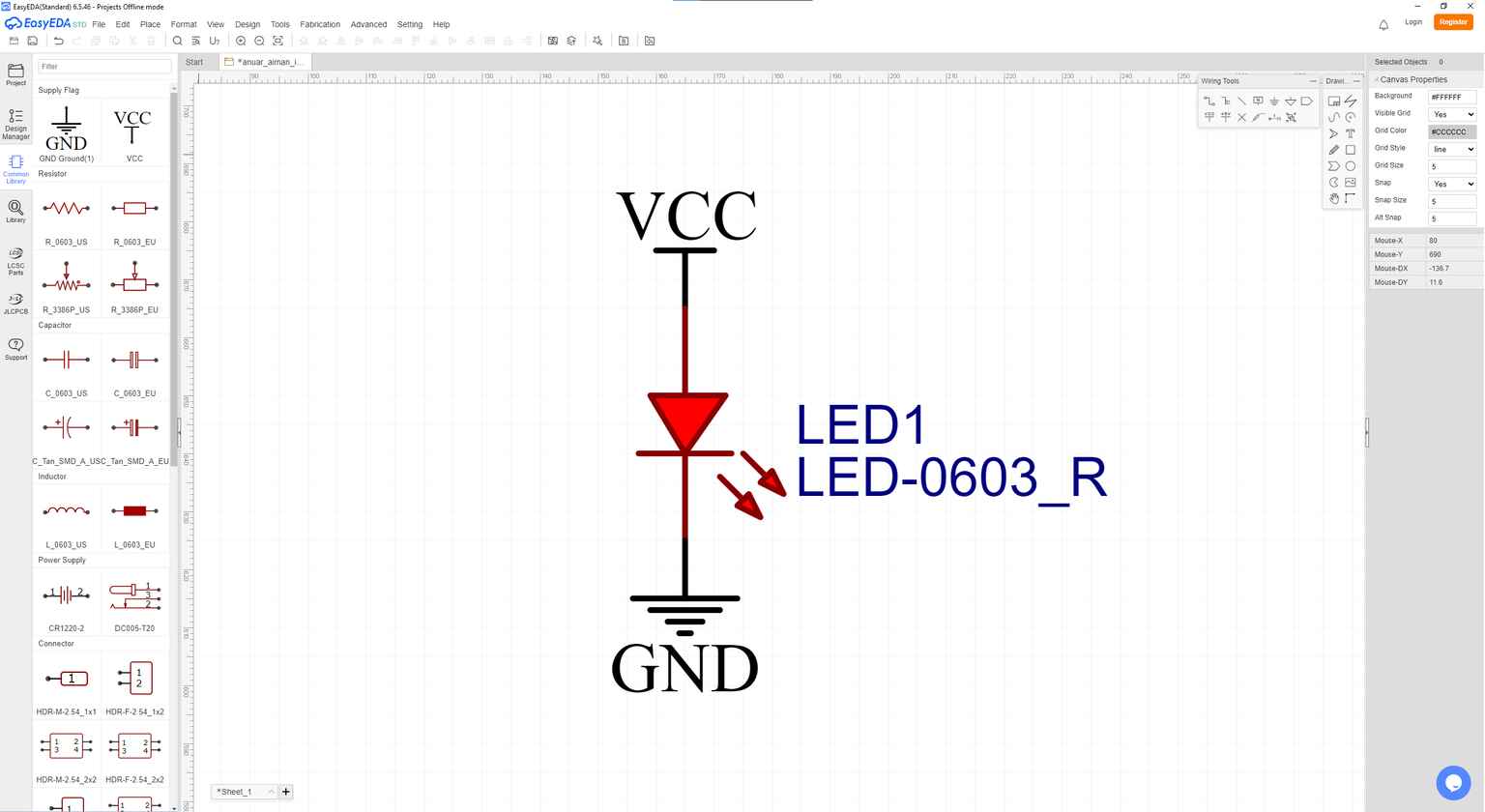
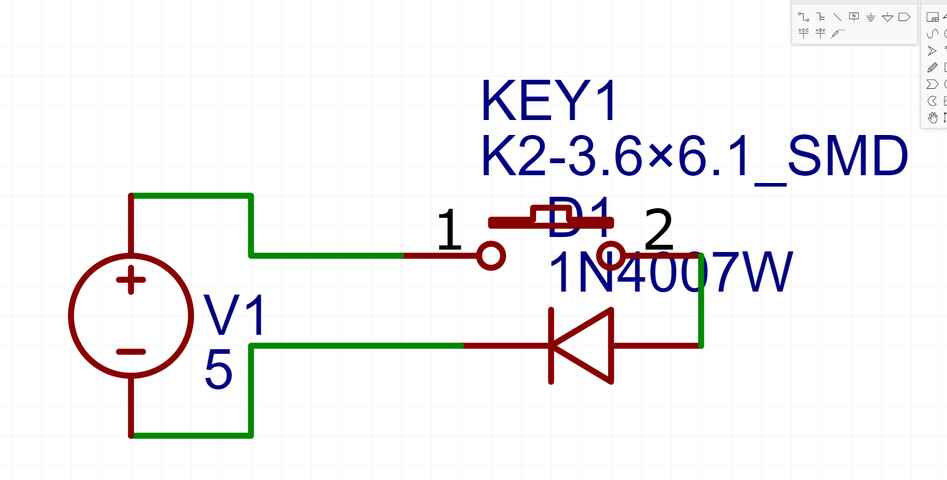
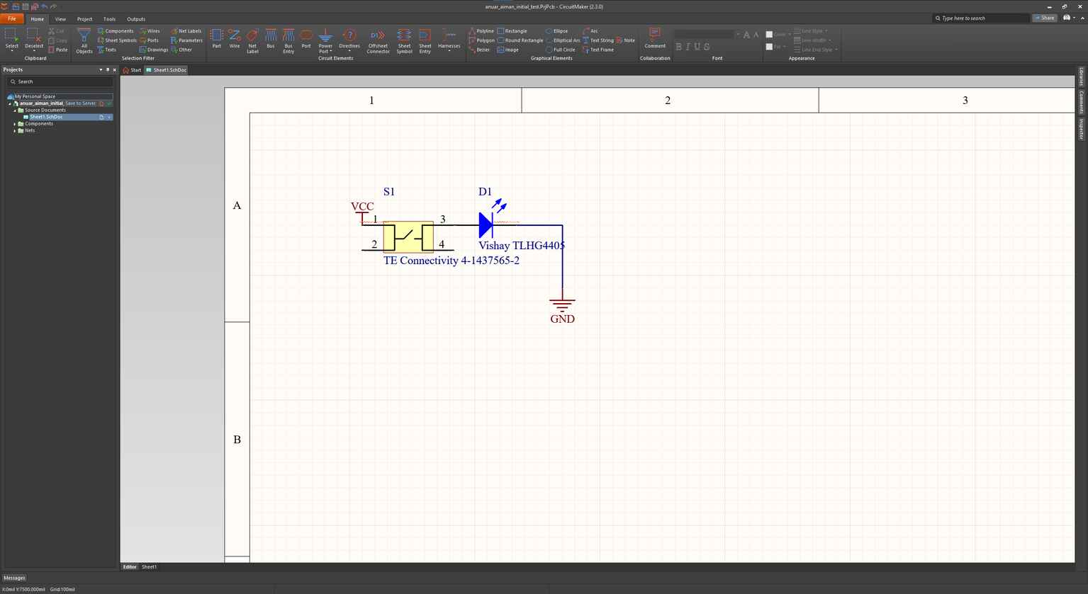
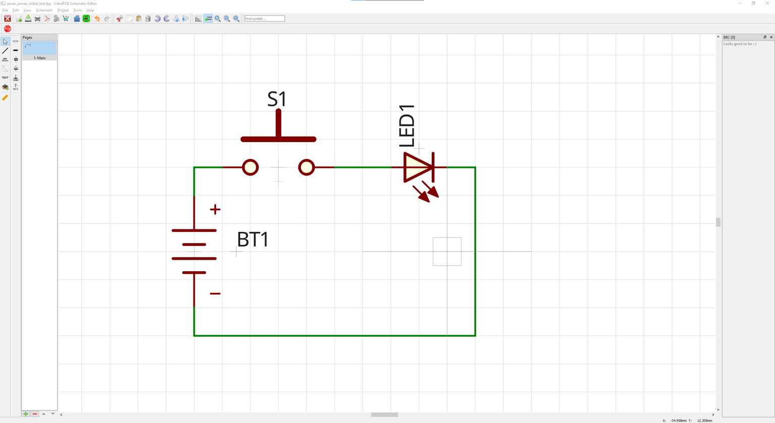
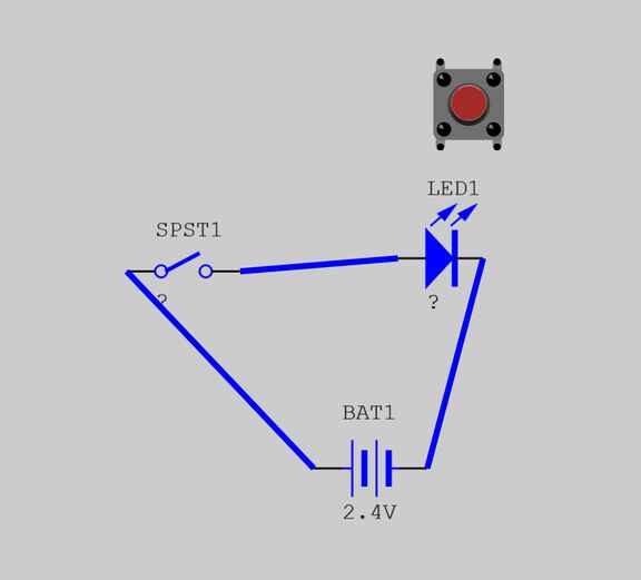
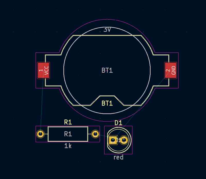
I tried making a simple LED and resistor circuit.
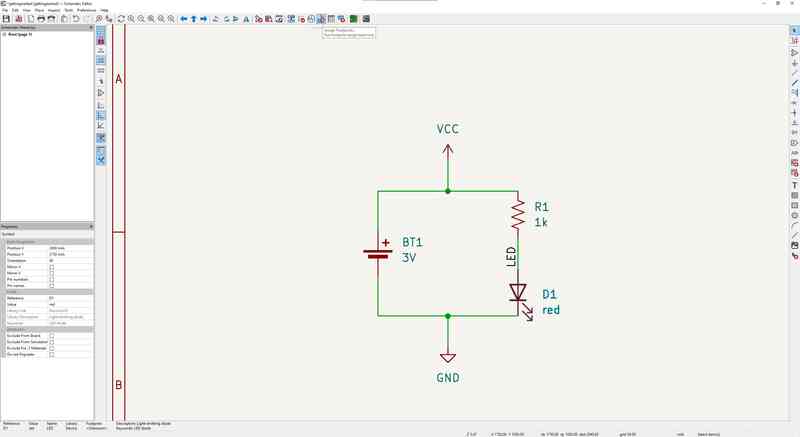
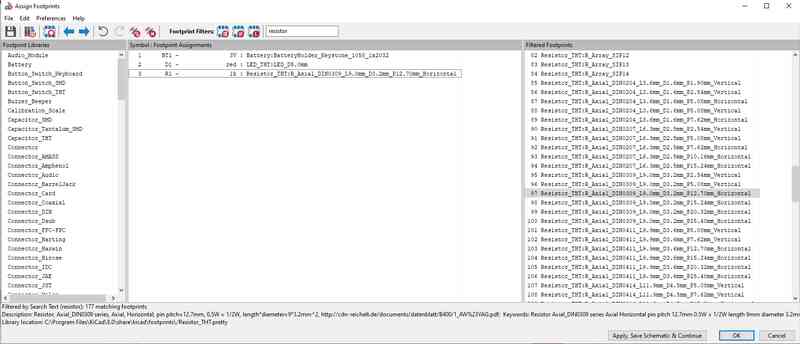
From there I tried to create the PCB so I needed to assign the footprint to each component in the schematic.
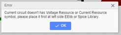
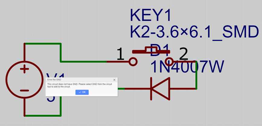
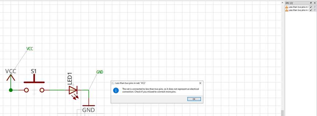
Before I could do that, however, I didn't pass the electrical rules check.
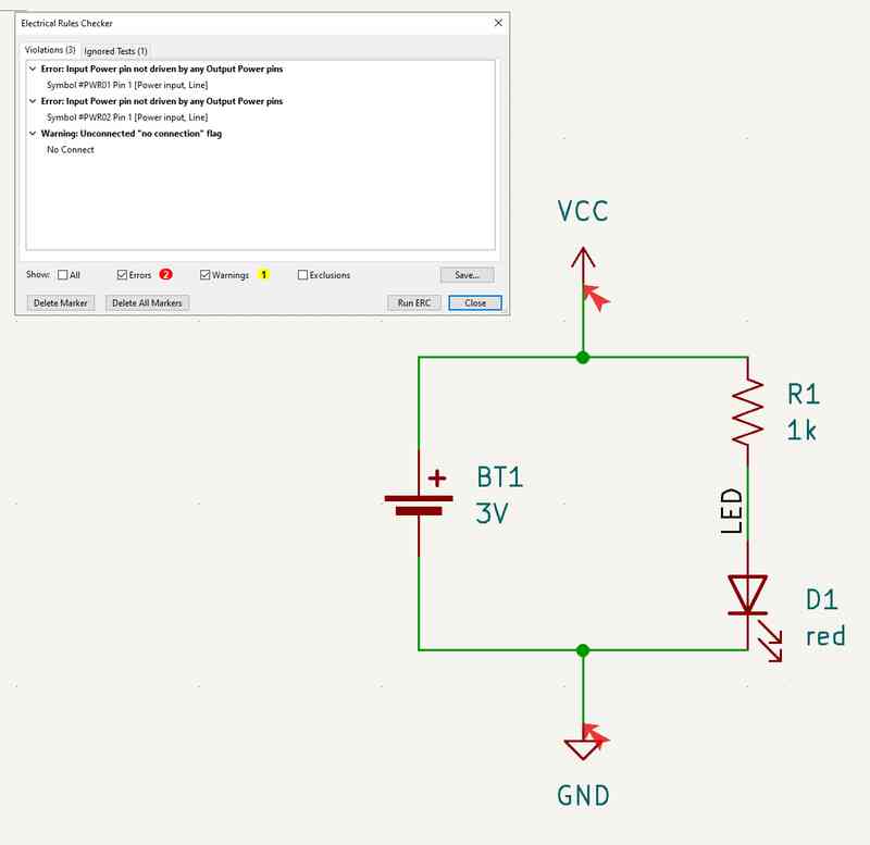
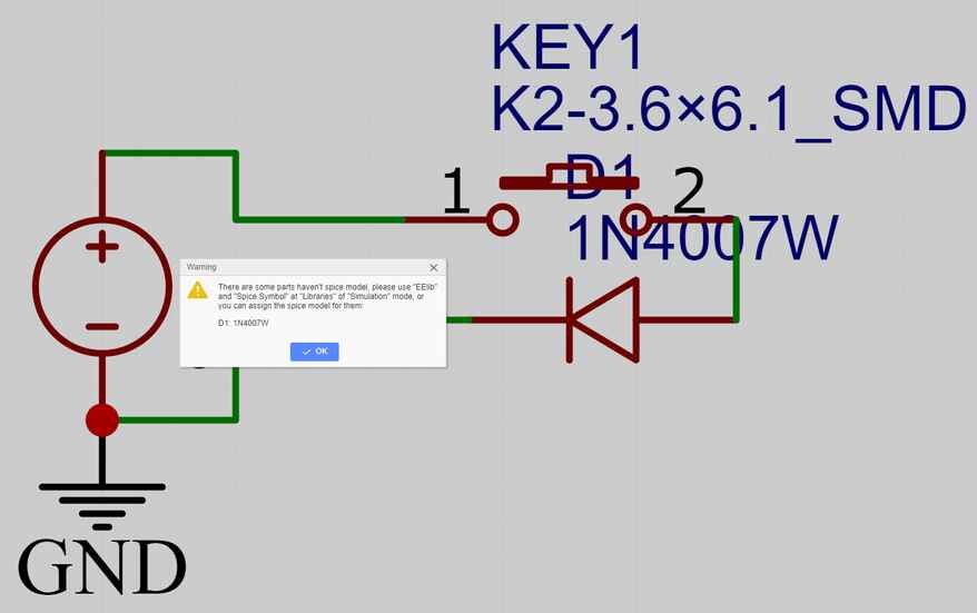
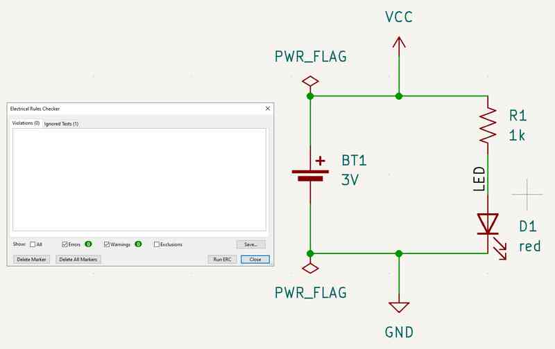
I solved this issue by adding power flags to each side of the battery.
Okay NOW I could do the footprint assignment.
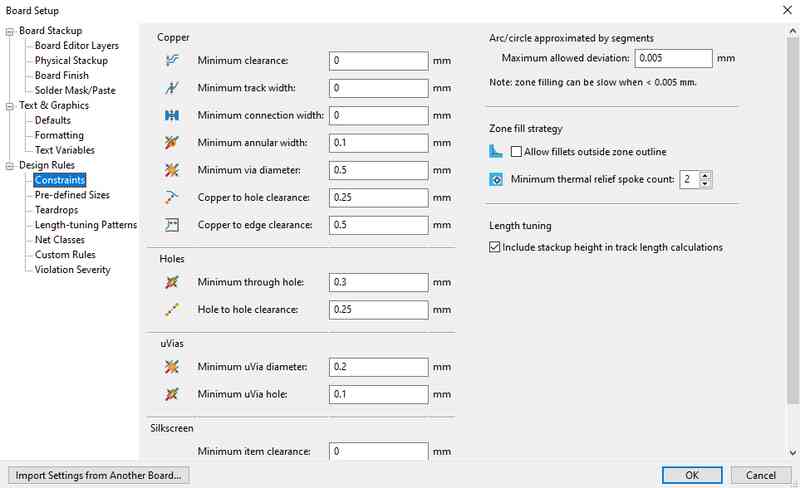
Here were the design rules I used. Note that in the future they would change to accommodate our mill's tolerances.
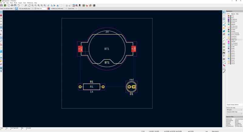
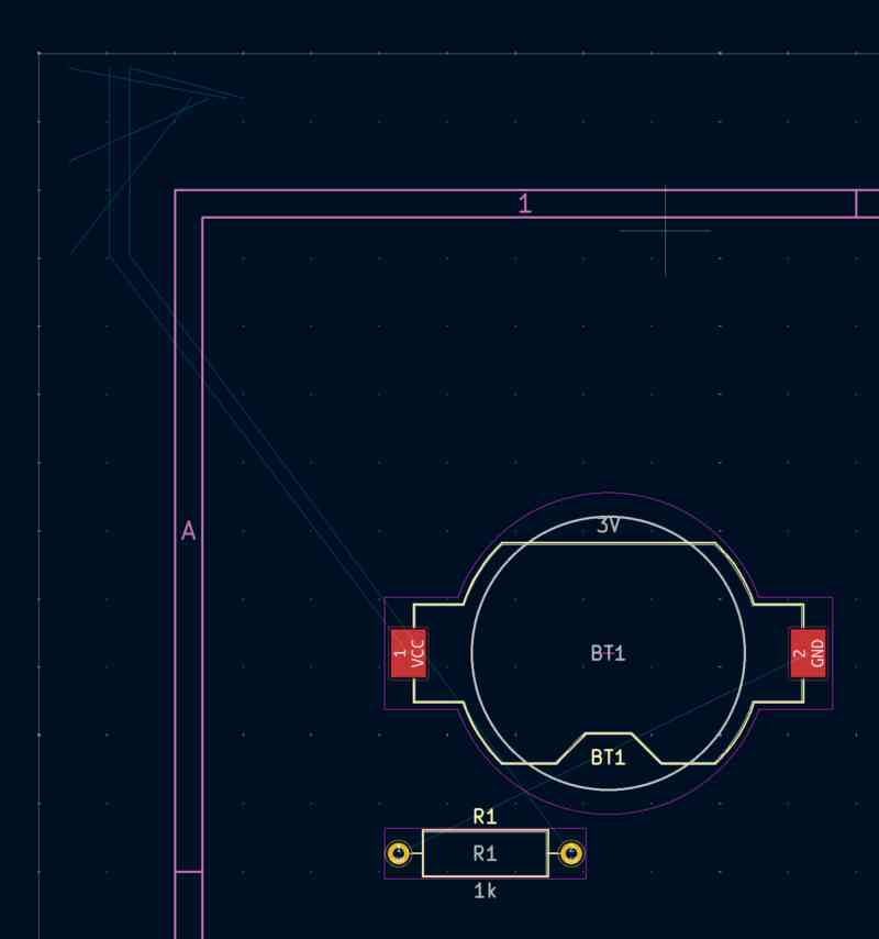
With the footprints assigned, I could now design the actual PCB!
Here's what the footprint initally looked like.
So I created the border of the PCB, a simple rectangle in the F. Cu layer.
I also had to define the back layer as a fill.
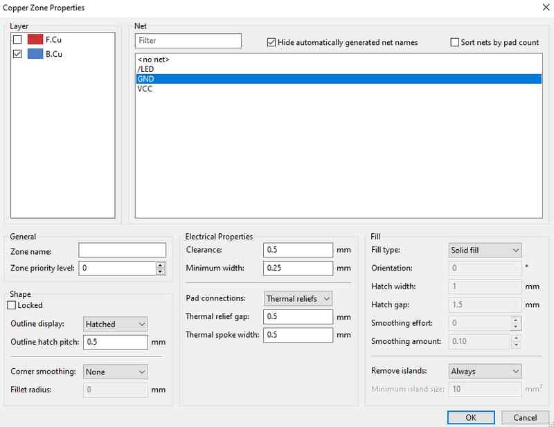
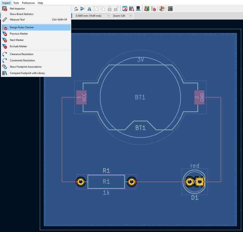
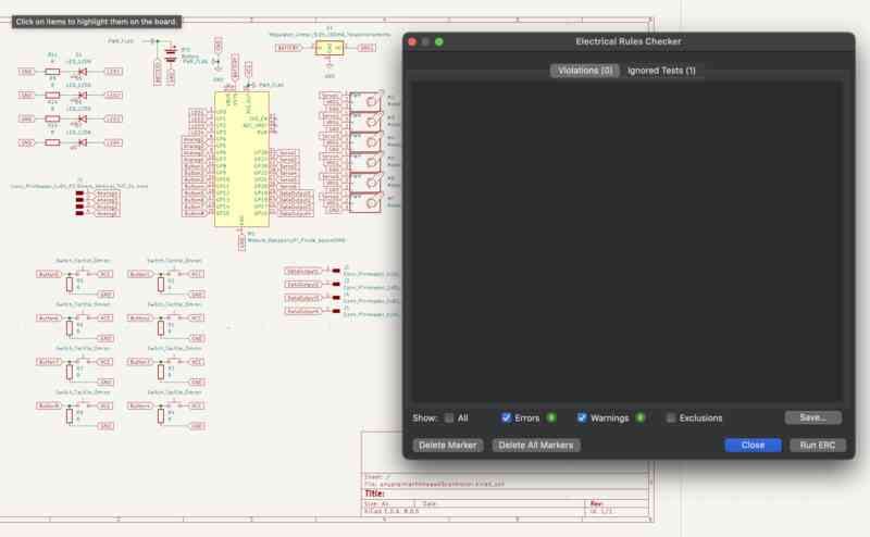
After arranging everything, including routing the traces around, and making sure all connections were connected, I checked my design rules.
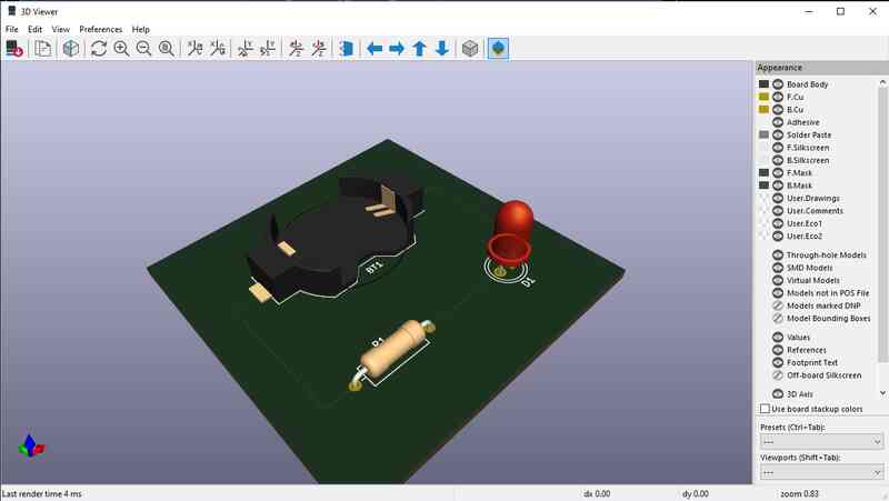
KiCad is cool because it gives you a model of what the PCB will look like when you fully assemble it!
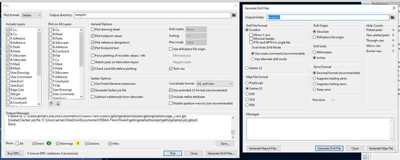
To cut the PCB out, you have to generate the drill files/gerber files.
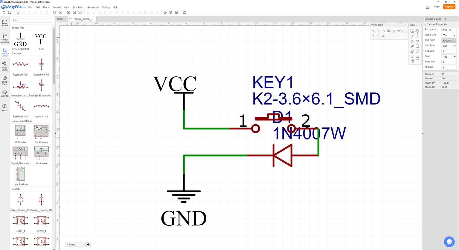
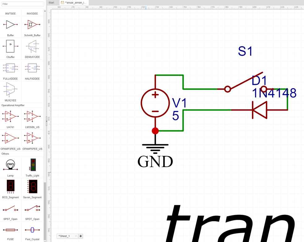
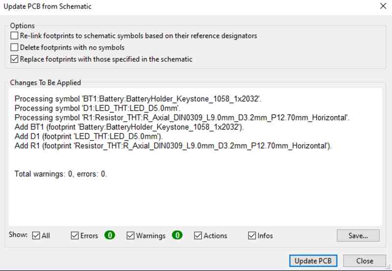
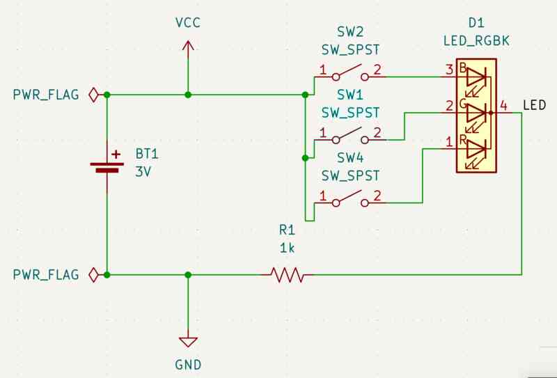
With the tutorial schematic finished, I decided to venture out into making my own schematic.
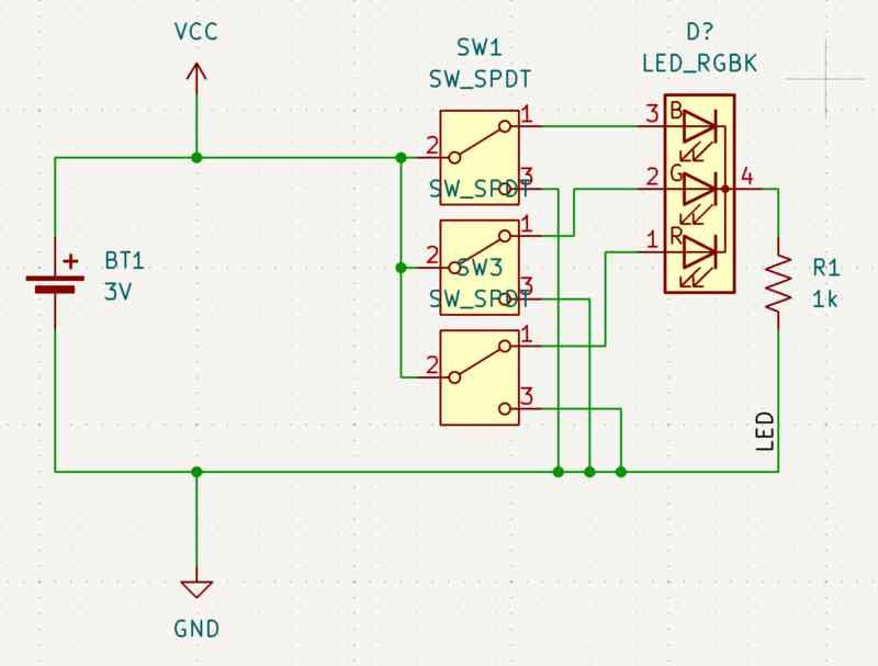
I decided to do something that had 3 switches that each could simply power each side of an RGB led.
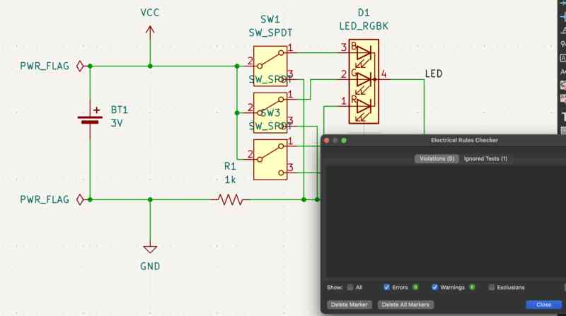
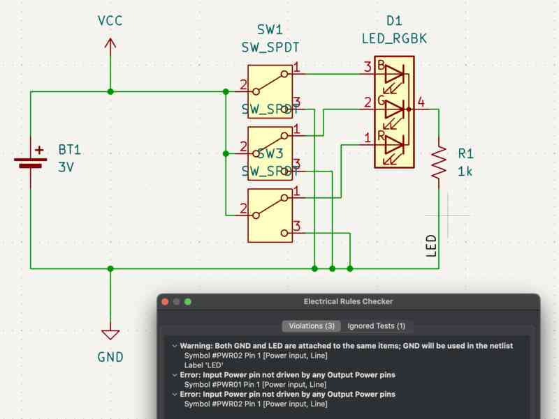
Of course I had to add power flags to solve an issue with the electrical rule check.
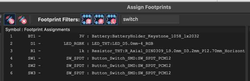
Okay NOW I could do the footprint assignment.
Of course I had to add power flags to solve an issue with the electrical rule check.
These are the footprints I assigned it.
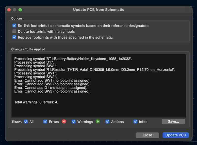
When everything loaded in, the traces all looked kinda weird and some components were simply not loading in.
I realized the SPST switches I used didn't have a footprint, so I had to find one for them.
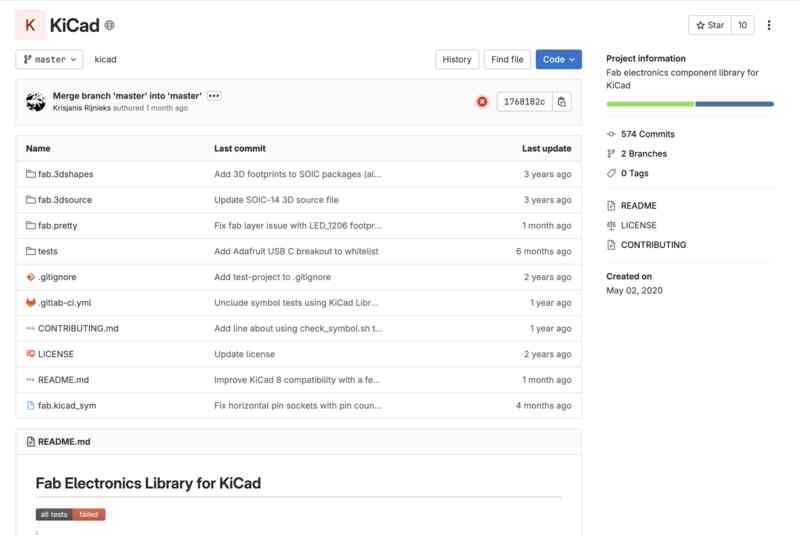
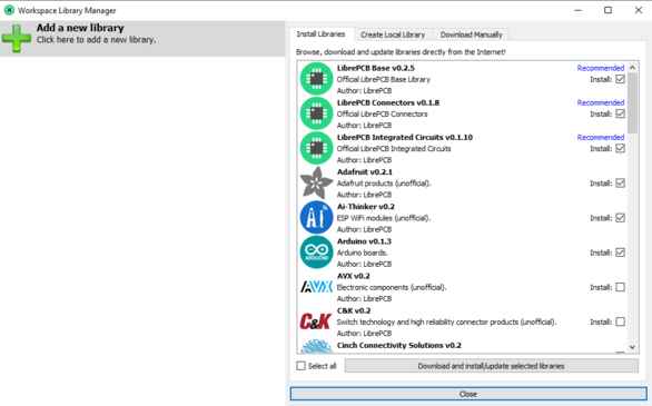
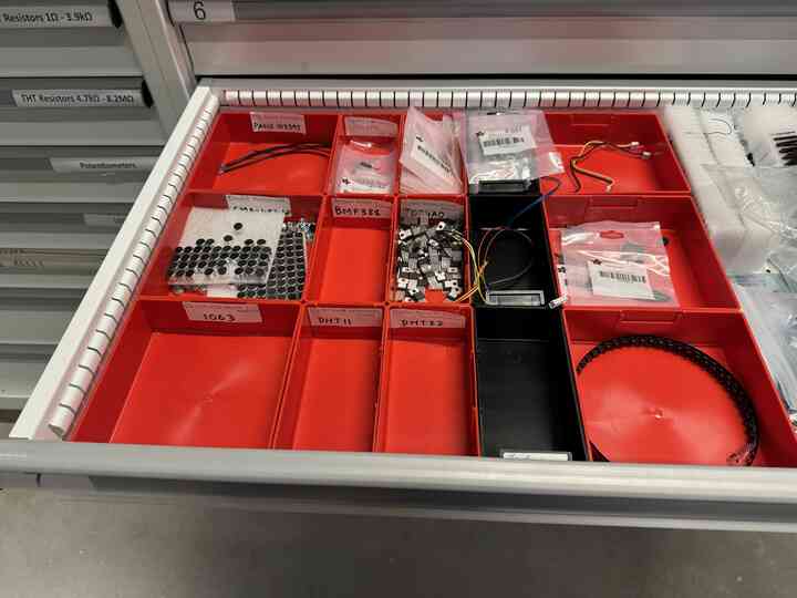
I downloaded the Fab Electronics Library for KiCad so that I could use the components from our inventory in the PCB design. It was also at this point that I realized (or I was told?) that I had to do a PCB with a microcontroller in it.
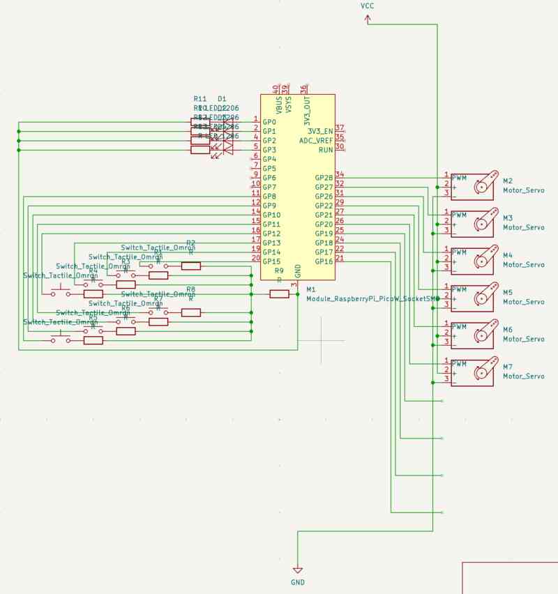
So I decided to place a PicoW as my microcontroller of choice, and design it as a multi-use controller, with multiple inputs and outputs. It would have 8 buttons, 4 LEDs, 6 servos, 4 data in, and 4 data out pins.
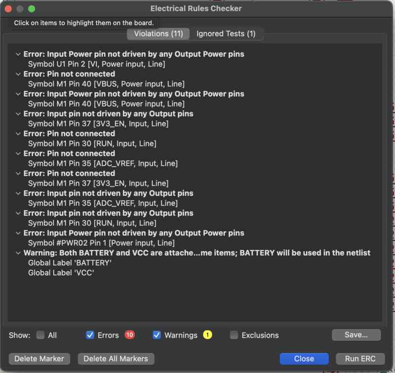
I had A LOT of electrical rules I had to solve in various ways, such as making sure that power flags were everywhere and that pins on the Pico without connections were marked as such.
It was at this point that Leo informed me that instead of using wires to connect everything, I should just connect them using labels, which would declutter the schematic.
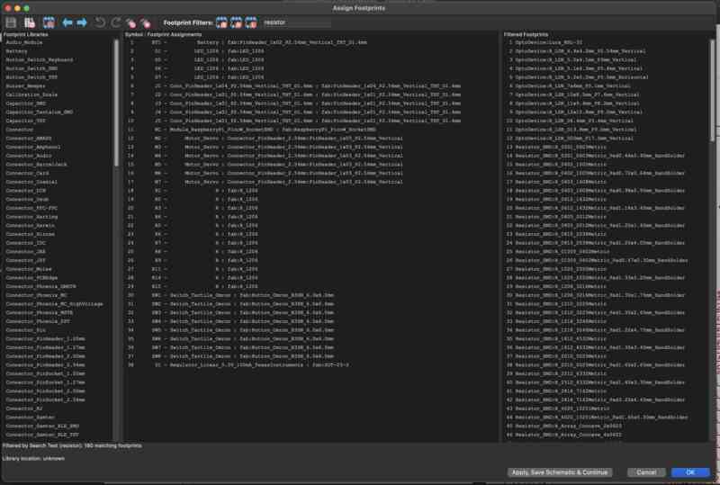
Yay for more footprint assignment...
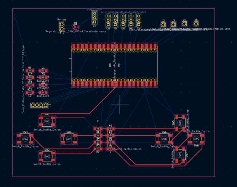
Here's how I arranged my PCB initially, sort of like a game controller. It looks nice, but it looked like I had to do a lot of moving things around to avoid needing vias.
I decided to take inspiration from the Nintendo Entertainment System's controller layout in mapping the four directional buttons. I found these layouts here.
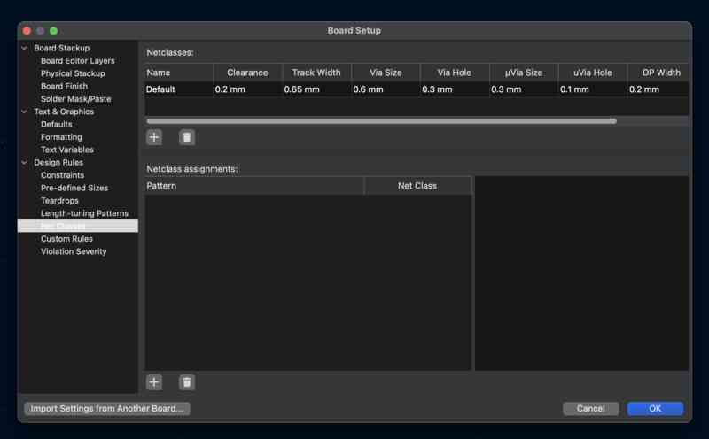
After laying out the controller, I adjusted the design rules to fit the specifications that others told me about, mainly track width of 0.65mm.
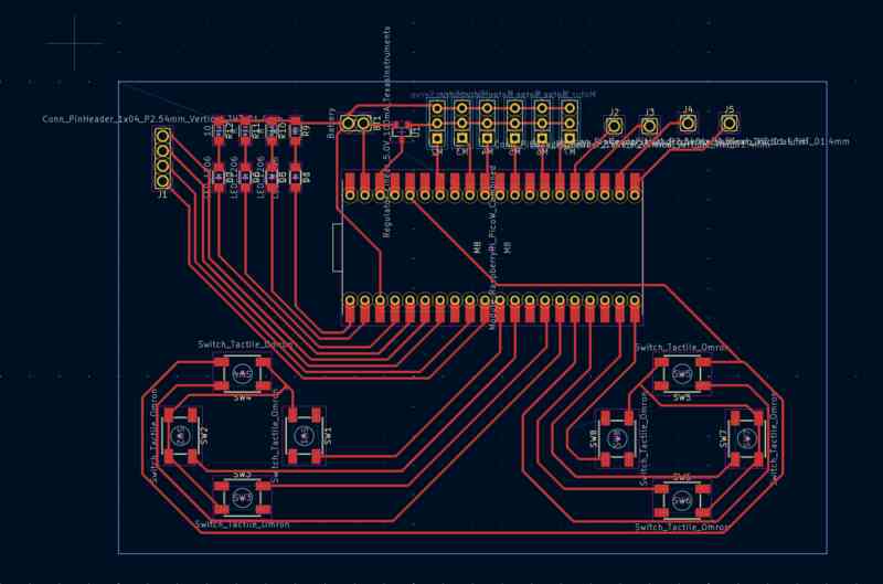
At this point I also realized I need to switch my microcontroller to a RP2040 to scale it down, but also that in general I could not do a controller as my first PCB to mill.
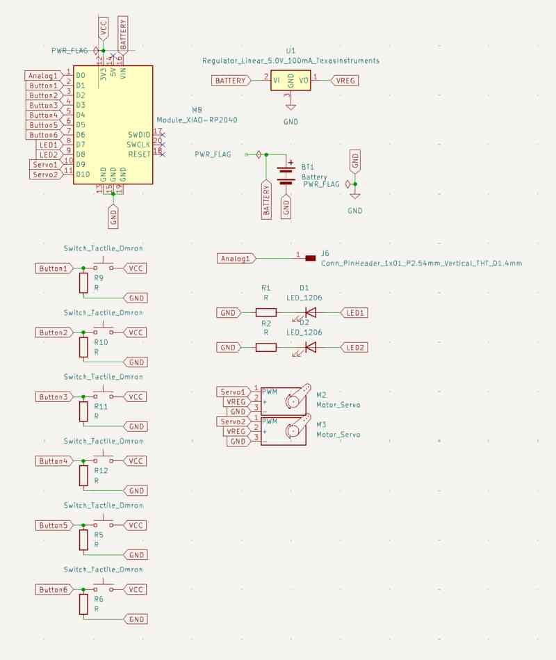
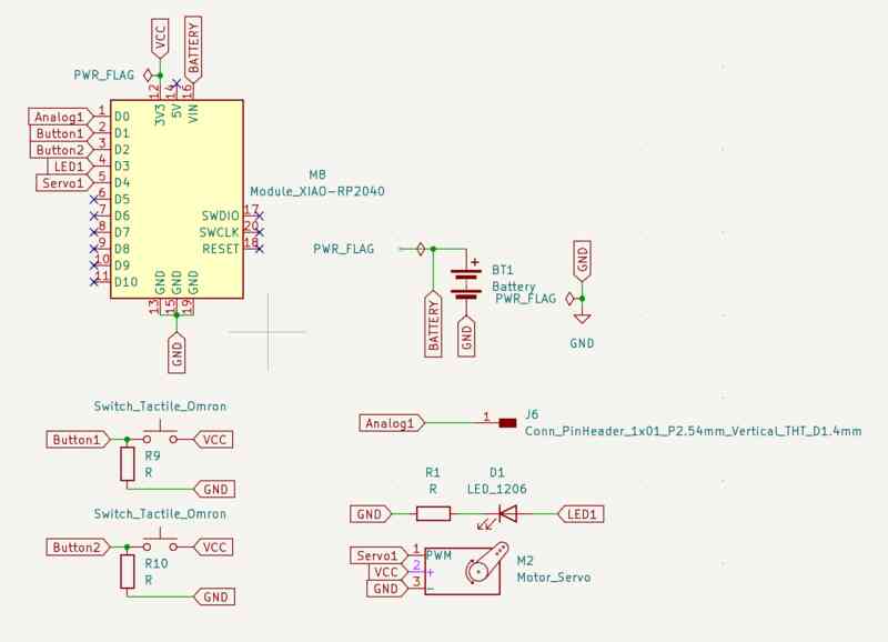
Here's the PCB schematic I designed for simple input and outputs from my RP2040.
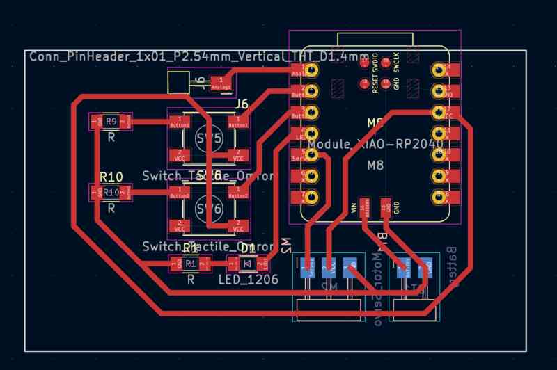
And that is the actual PCB (without components on it!)
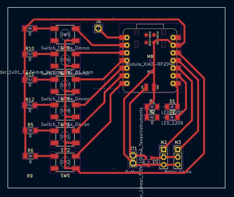
Leo told me I should simplify it even further, so I edited the schematic like so.
I arranged the actual PCB like so.
And that is where electronic design week ends! My reflection is that this was a new process to me, and even though I had worked with schematics in the past, I'd never designed PCBs before, so I'm glad to have gained this knowledge about how to design them. I definitely started out too ambitiously with my design and I could definitely learn to start my weeks with the small stuff.
Home