HTMAA 3024 - Week 5

Previous: Scanning and 3D Printing Home Next: PCB Milling

Week 5: Electronics Design

This week, we dove into the world of electronics design, focusing on creating custom PCBs using KiCAD. As a tool widely adopted in both academia and industry, KiCAD offers a robust platform for designing and simulating circuits. I was particularly excited to revisit PCB design, having previously worked with laser-based fabrication techniques at the Harvard Microrobotics Laboratory.

KiCAD Design Process

I started by creating a simple LED circuit to familiarize myself with KiCAD's workflow. Below, you can see the progression from schematic design to a fully routed PCB. Each step involved careful consideration of component footprints and connections, ensuring the final design was both functional and manufacturable.

KiCAD LED Circuit
Initial designs: A simple LED circuit created to test KiCAD's capabilities.
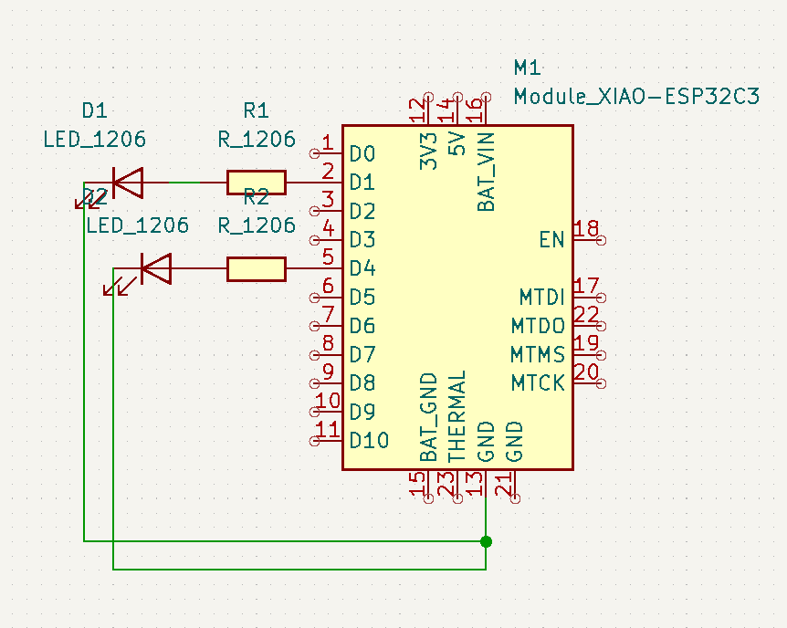
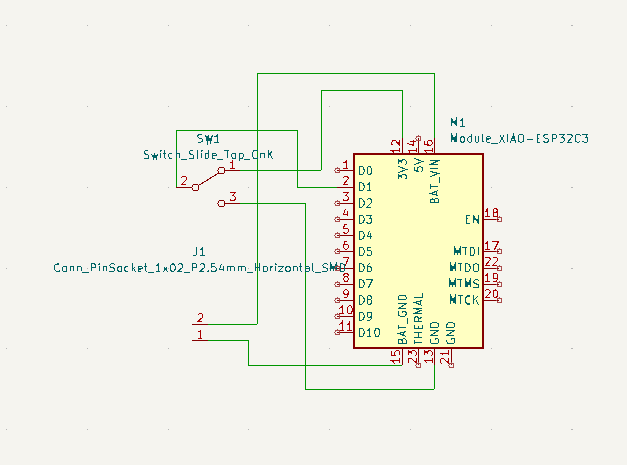
KiCAD Schematic
Schematic: A detailed view of the switch circuit with all connections mapped out.
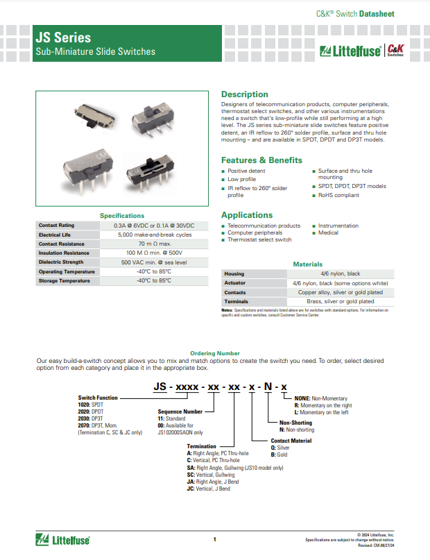
Component Datasheet
Datasheet: Reference for component footprints and specifications.
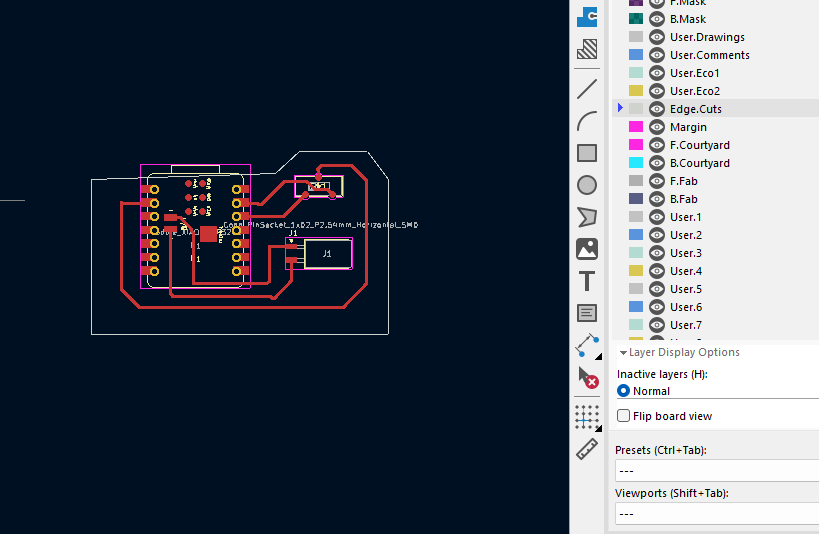
Fully Routed PCB
Final PCB: The fully routed circuit, ready for fabrication.
Fully Routed PCB
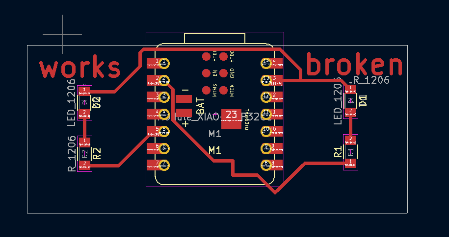
In the end I remade the LED circuit to be an indicator.
Fully Routed PCB
Text on the silkscreen looks nice!.

Group Assignment: Testing Equipment

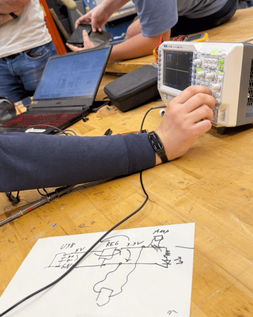
For the group assignment, we used lab equipment to observe the operation of a microcontroller circuit board. This hands-on experience helped us understand the importance of testing and debugging in electronics design.

Fully Routed PCB
Final PCB: The fully routed circuit, ready for fabrication.

Assignment