Week 6: Milling a PCB on the Carvera
This week, I delved into the world of PCB fabrication using the Carvera milling machine. My goal was to design, mill, and assemble a functional LED circuit. The process involved designing the circuit in KiCAD, exporting Gerber files, and meticulously milling the board on the Carvera. Below, I’ve documented each step of the journey.


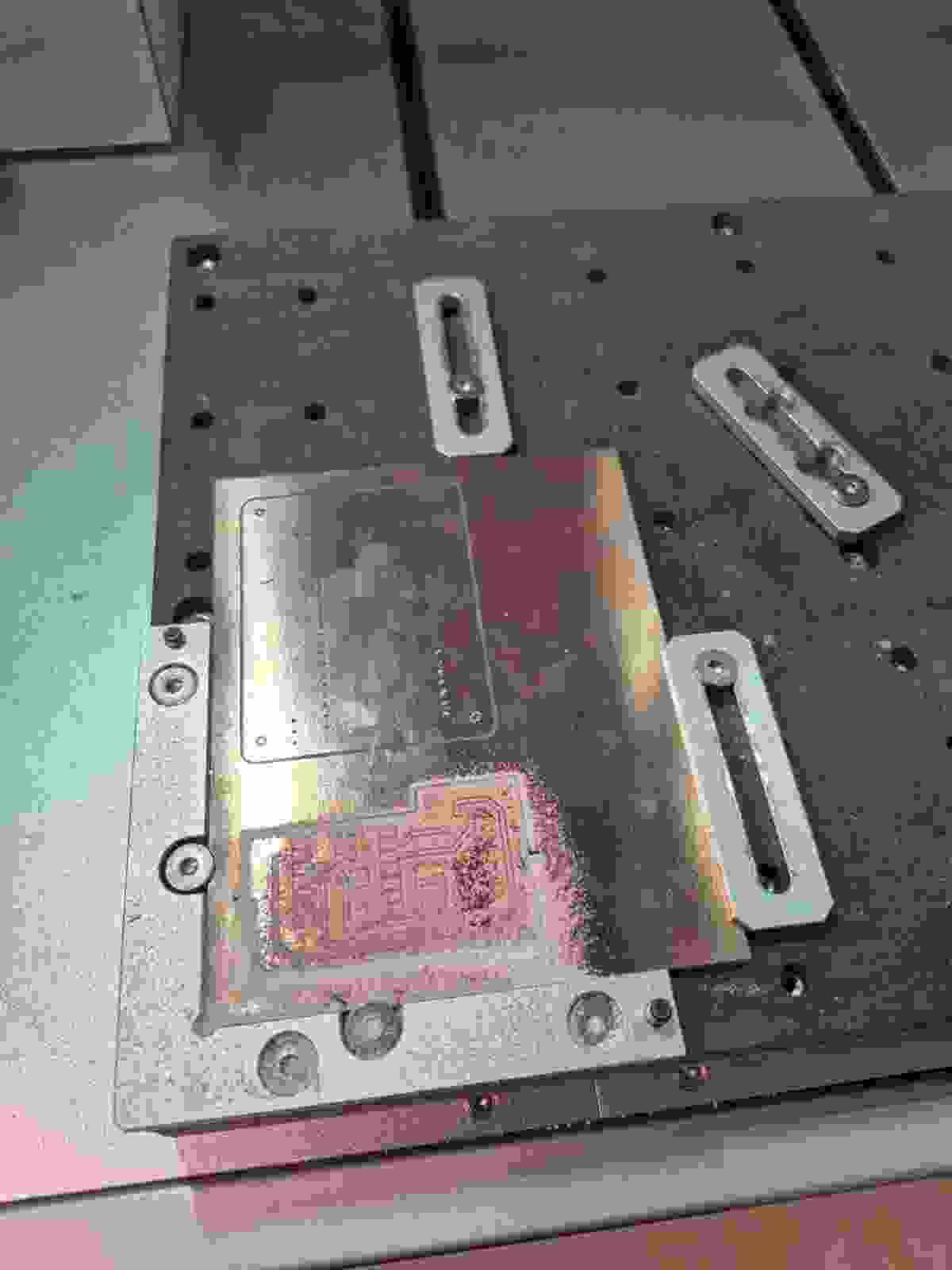
After completing my first attempt, I was eager to refine the design and create a more polished version of the PCB. This time, I focused on improving the precision and aesthetics of the board.
.png)
.png)
.png)
.png)
The MODS interface proved to be intuitive and efficient, generating tabs and G-code for the milling machine seamlessly. This streamlined the process and ensured accurate results.
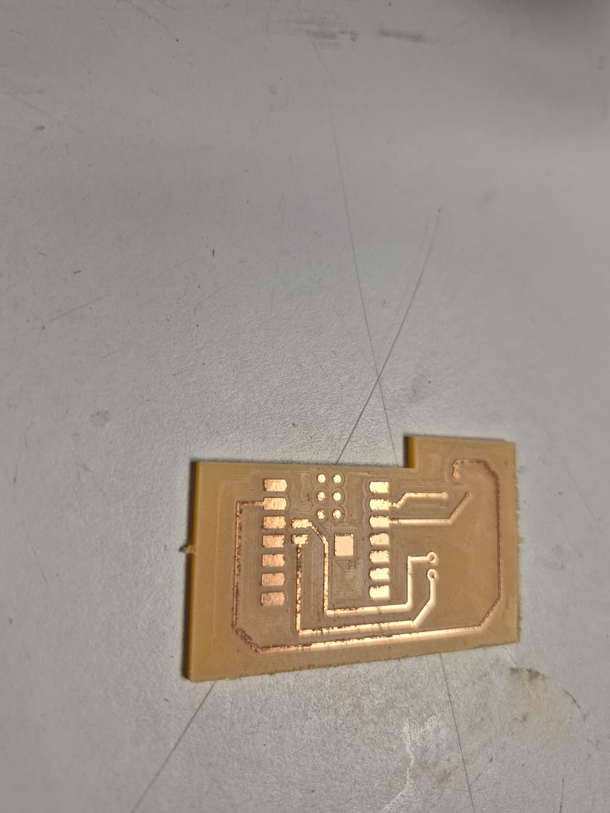
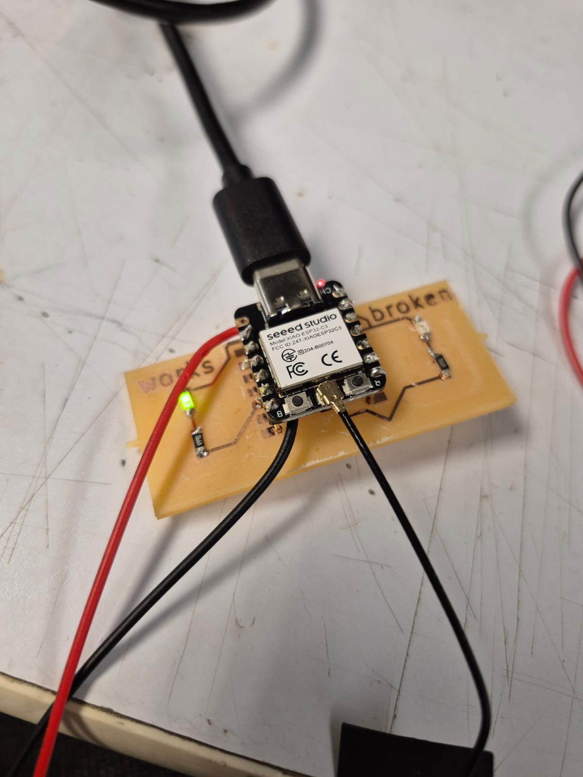
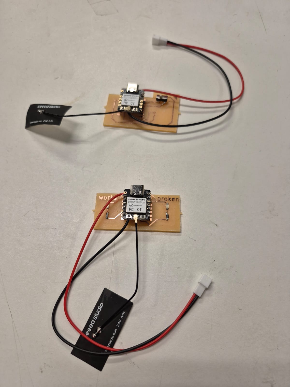
The final result was a clean, functional PCB with no issues encountered during the soldering process. The experience taught me the importance of precision and attention to detail in PCB fabrication.