HTMAA 25
home about me final projectThis week’s task was to make and test an embedded microcontroller system we designed. I’ll primarily be trying to make my brain board from last week.
We milled the test board to find minimum trace widths and clearance. The minimum trace clearance was trivially the endmill size (1/64in or ~16mil), while the minimum trace width was ~9mil. Full documentation can be found here.
After reviewing my board with the amazing Anthony, I was told that I needed to increase the width and thermal width parameters on my ground pour. This broke a few places where I was routing ground through narrow gaps, so I had to decrease the width of a trace passing through connector pads to 14 mil, and set the board outline clearance design rule. This design rule I learnt would be useful if we were designing for FR4 boards, but is irrelevant for our FR1 milling process, and so decreasing it would allow me to nudge traces closer to the edge.
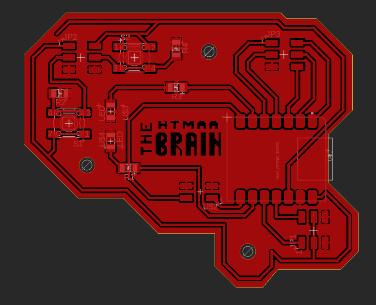
I also took the opportunity to redesign my center text from a vague abstract think to a more appropriate the brain, htmaa.
Upon putting it in the machine though, I was surprised to find a milling time of 55m — after all, I’d just watched a 20-minute mill for a larger board, and I had class in 40 minutes! It turns out that it was because my trace-trace distances were 16mil, and so it was using the smaller, slower 1/64 tool for all of them. If I made them wide enough for a 1/32 endmill to pass through, I could potentially cut down my machine time.
However, I couldn’t just change my trace-trace minimum distance to be 32mil in the design rules, since some parts of my board required the smaller clearances to work. I decided to deal with this by setting the Isolation property on my ground pour to 32mil, then creating another ground pour over the clearance-sensitive parts with an isolation of 16mil.
While waiting for the mill again, I also changed the footprints from the default 1206 footprint to the fab1206 footprint, which increased the width between the solder pads and extended the solder pads a little beyond the component for easier solder iron use.
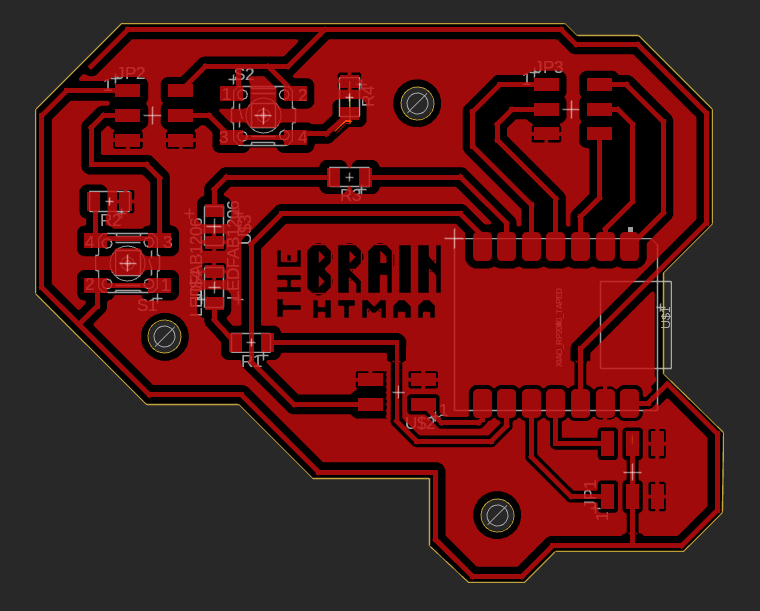
The result is much less aesthetically pleasing, unfortunately — but it takes less than 18 minutes to mill!
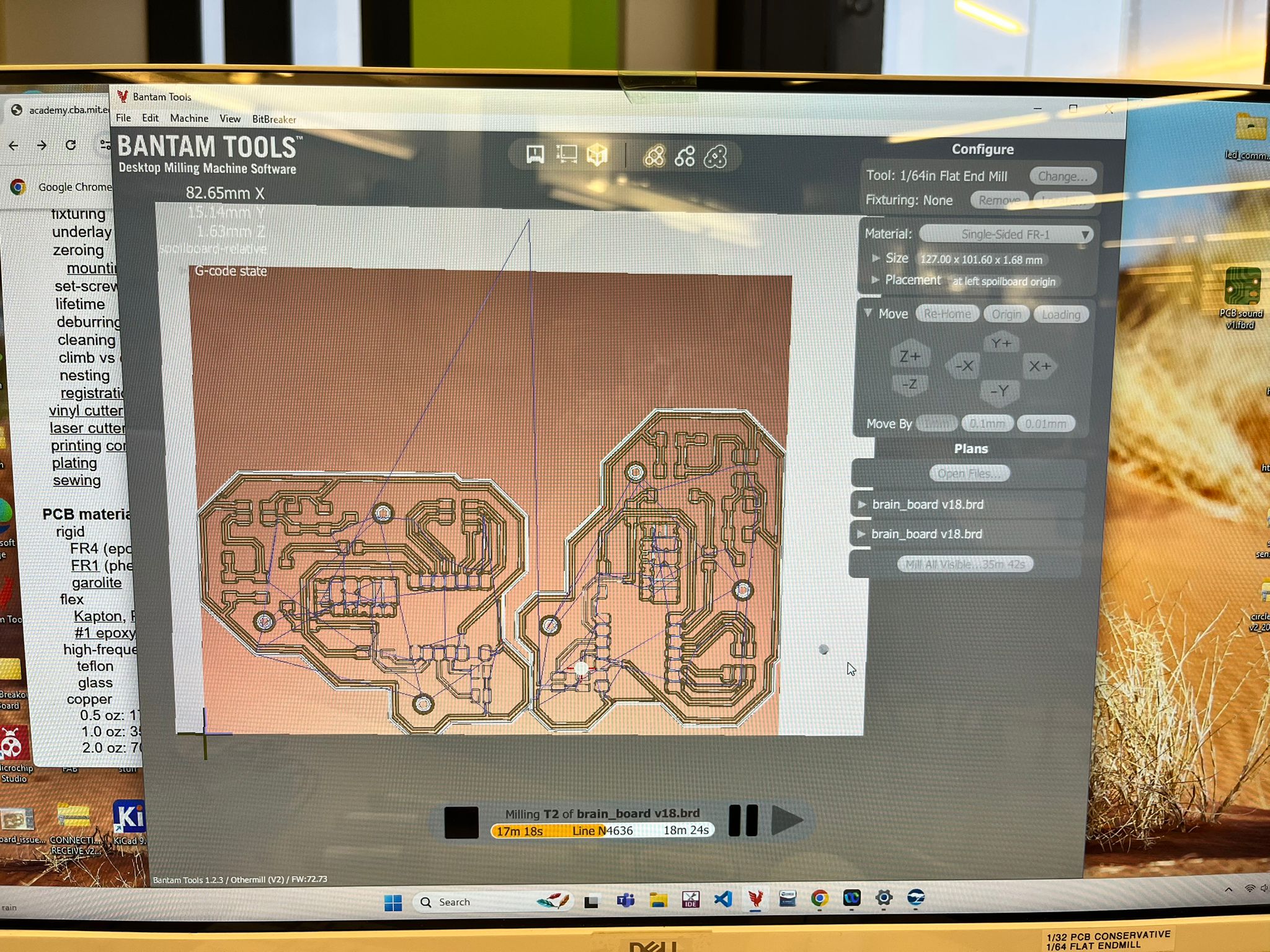
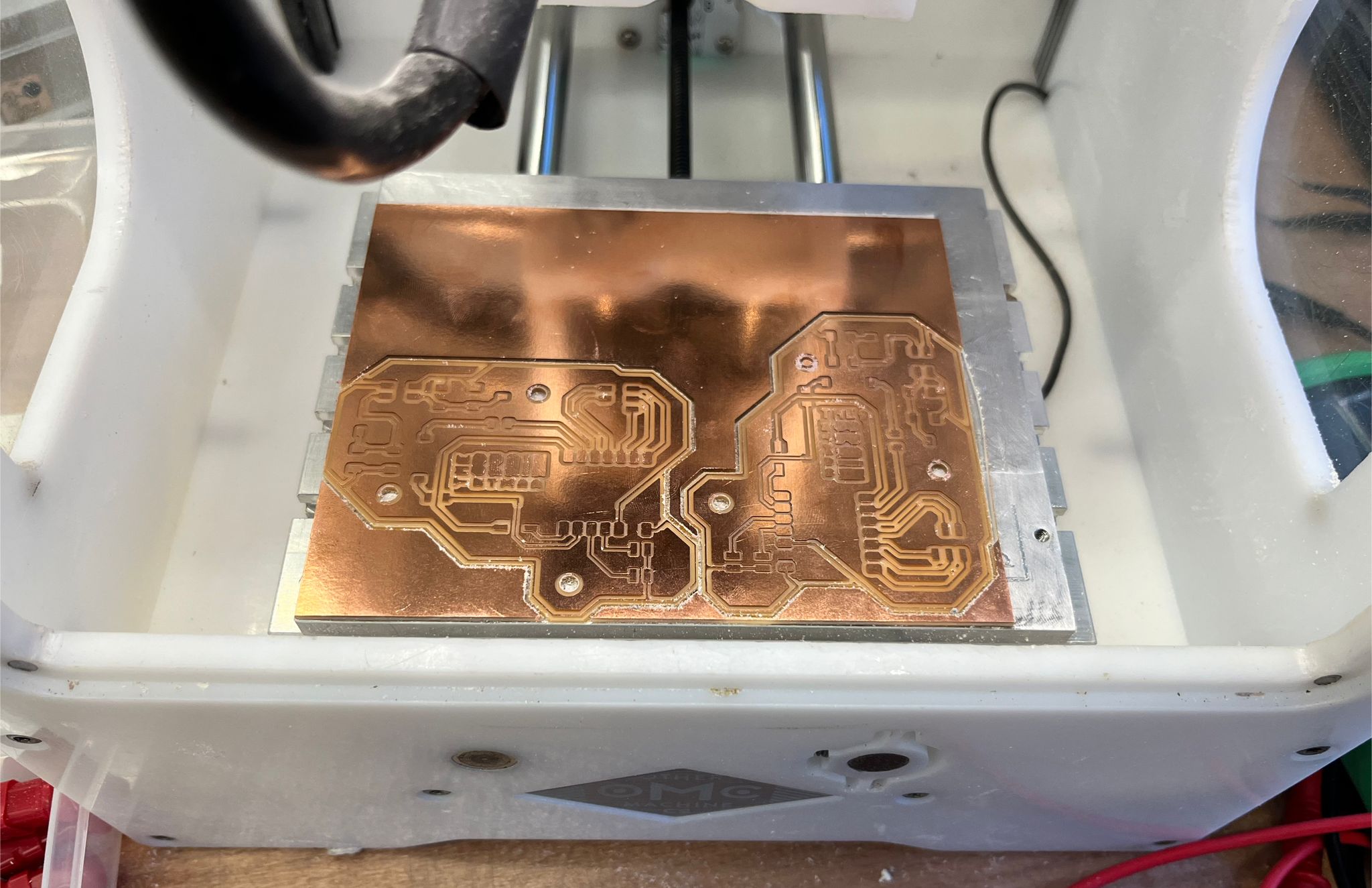
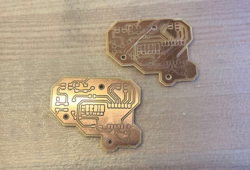
I heeded advice from a classmate in my section and milled 2 copies of my PCB on the Othermill, in case I messed up soldering and needed a second copy. They fit surprisingly perfectly on the copper stock, and take a combined time of ~36 minutes. I used the 1/64 tool first, followed by the 1/32.
After taking out the boards, I tried to scrape the surface of the PCBs with a metal edge, but ended up scratching one of the boards. Since the scrape didn’t go through the copper layer, this is largely an aesthetic issue.
To be completely honest, I’d forgotten I had to choose resistor values. Pulling up the datasheet for the LEDs we have in shop, we find that the forward voltage is 2.1V and the current is about 20mA. Since the pin voltage is about 3.3V, we expect a 1.2V drop across the resistor, which gives us an optimal resistance value of 1.2V/20mA = 60 ohms.
I mentioned this in passing to Anthony, who declared that unless I was actively trying to make the LED as bright as possible (also difficult to look at directly), this math was entirely useless and I could just put a 1kΩ resistor on. 1kΩ resistors it was.
Somewhat arbitrarily, I will go for one red and one green LED.
My final assembly component list thus includes:
I started by soldering the microcontroller, then all my 1206 components, then switches, then connectors. Without solder masks, this was a much more frustrating soldering experience than I’m used to. I noticed only as I was soldering that my thermal reliefs did not get milled, so half of my ground pads turned into large, running pools of solder. Solder also often jumped the spacing between traces, and while this wasn’t an issue for the 32mil-spaced sections of my board, it did lead to a good few solder bridges in the 16mil-spaced section.
Nonetheless, here is my completed board:
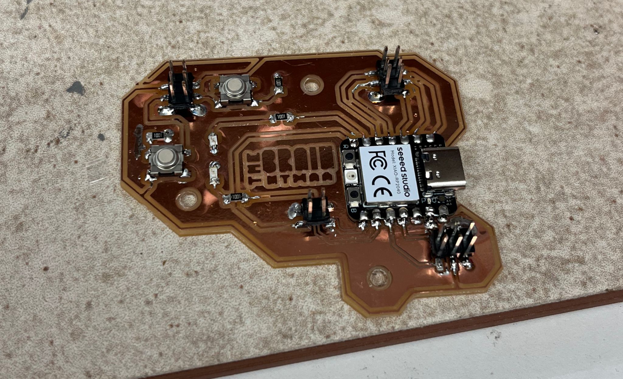
I then used a multimeter on continuity test mode to test connections between all microcontroller-connector pin pairs, and to test that the ground plane was entirely connected.
With a couple of female-female jumper wires, I wrote the following test program to turn on the LEDs when the buttons are pushed.
#define LED1 2
#define LED2 7
#define SWITCH1 29
#define SWITCH2 28

void setup() {
  pinMode(LED1, OUTPUT);
  pinMode(LED2, OUTPUT);
  pinMode(SWITCH1, INPUT);
  pinMode(SWITCH2, INPUT);
}

void loop() {
  digitalWrite(LED1, digitalRead(SWITCH1));
  digitalWrite(LED2, digitalRead(SWITCH2));
}
And it works!
Making a simple PCB is actually a lot more straightforward than I thought it would be, and I now have a neat little breakout board for an RP2040. Some things I would have wanted to do this week if I had more time: