Week 5 — Electronics Design
okay so for my final project i want a WebXR experience on my Quest 3. i’m also doing an independent study with my advisor (Takehiko Nagakura) to collect/clean Gaussian Splat files and turn them into shareable WebXR scenes. last week i compared different camera types and tried importing GS into a few engines, mainly PlayCanvas + SuperSplat, so i can share/view it. with SuperSplat’s viewer app i can literally export an .html and host it on our server (see: this link).
idea: the MagKey cassette → headset pulls a scene
for the course final i want to pair it with that study.So the user can just sit next to a table, put the headset on, place a tiny 3d-printed “MagKey Cassette” on a little platform, and the headset fetches a specific WebXR URL. kinda like a spatial Walkman, you can bring a place with you and jump in whenever you want.
sensor plan for this week
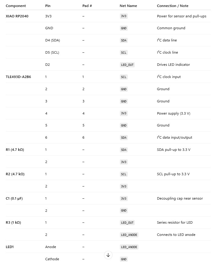
i asked chatgpt what’s a good tiny starter piece for the cassette idea for this week when I'm starting to learn about PCB for the first time. answer was: magnet pattern + Hall sensor. so: use a small magnet and a 3D hall sensor, detect presence over I²C, toggle an LED first. from the class inventory i found the Infineon TLE493D-A2B6 (Digi-Key p/n TLE493DA2B6HTSA1) and checked if it plays nice with the Seeed XIAO RP2040, and gpt said yes (it even told me how to do i simple breadboard check but i wasn't able to get there this week).
- MCU: Seeed XIAO RP2040
- Sensor: Infineon TLE493D-A2B6 (3D Hall, I²C)
- Library: fabcloud KiCad library
- Firmware: Arduino IDE
parts list i used:
- XIAO RP2040
- TLE493D-A2B6 (or breakout)
- 2× 4.7 kΩ I²C pull-ups
- 1× LED + 1 kΩ series resistor
- 1× 0.1 µF decoupling cap (VDD↔GND at the sensor)
- small neodymium magnet (3–5 mm)
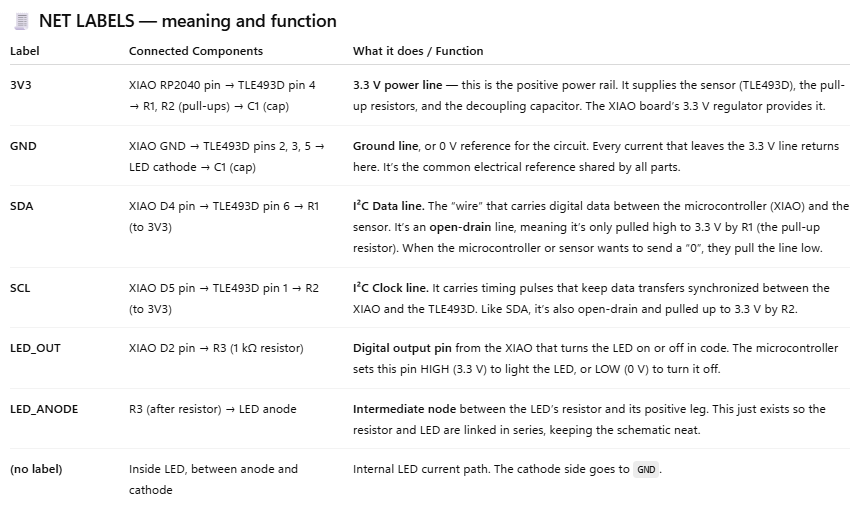
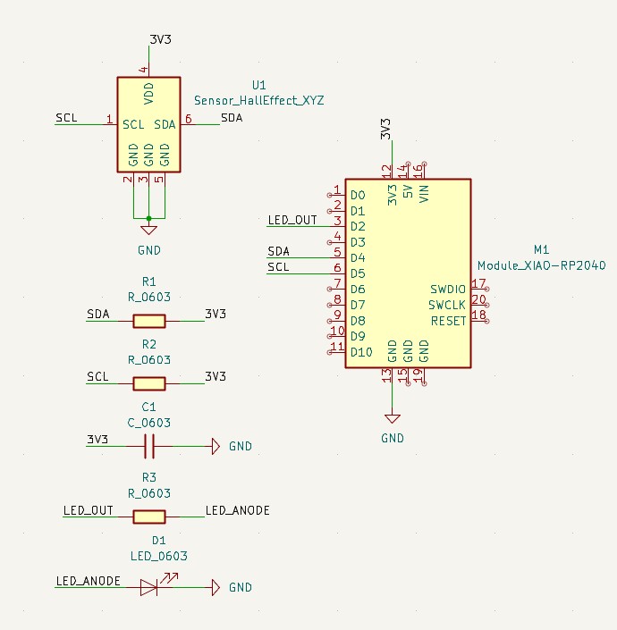
Net labels that actually made things click
The wild helpful part was gpt handing me a set of net labels with what each does. made wiring the schematic way less scary.
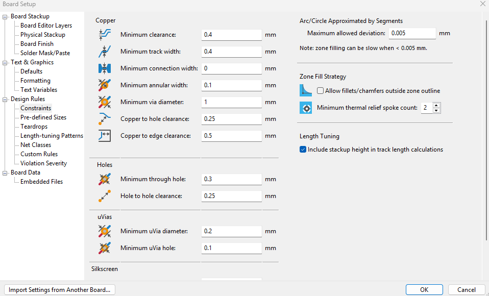
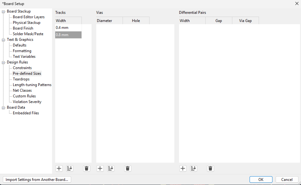
Board setup
Just followed last thursday’s recitation and set the rules.
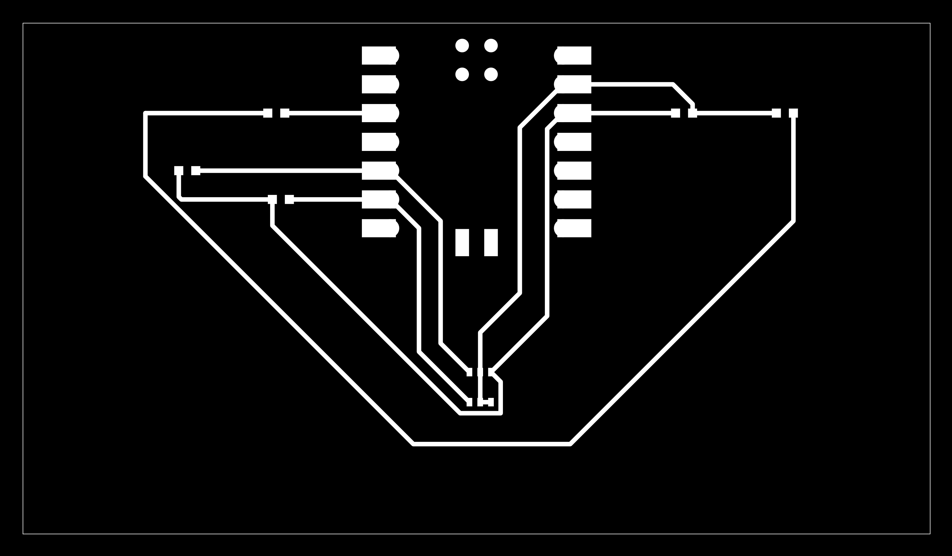
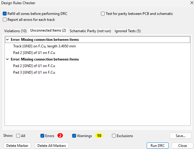
Errors → Fix
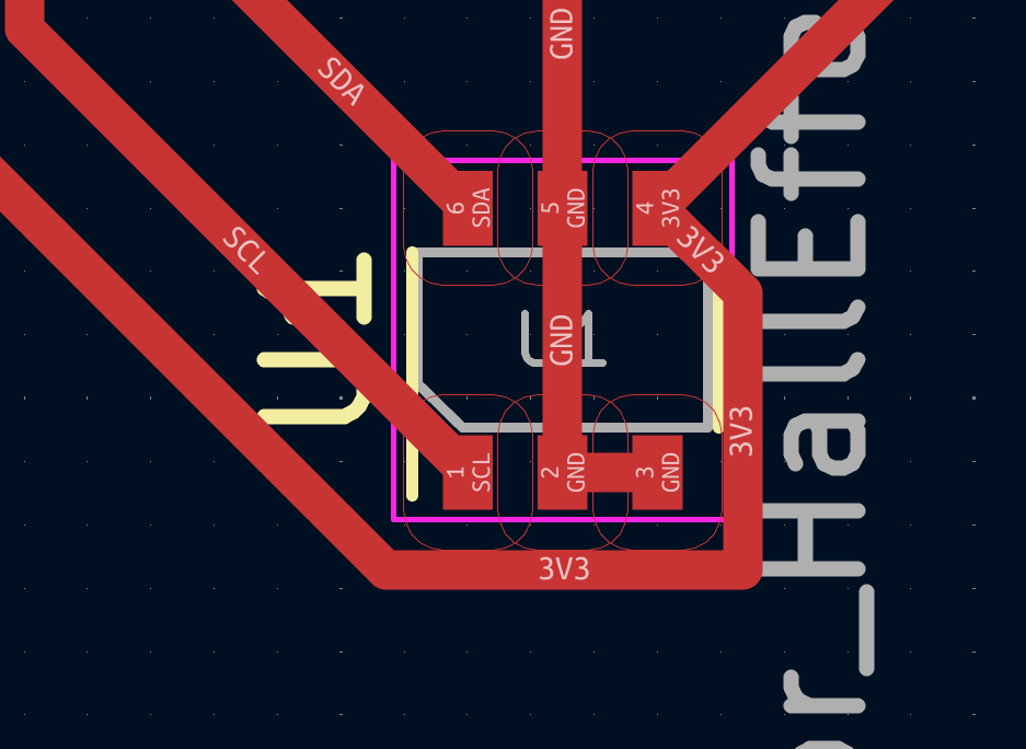
Following the recitation tutorial, I ran Design Rule Check before I exported the file and it complained. Turned out i missed a tiny internal GND connection on the hall sensor footprint. Those are small details that were really hard to catch without a the DRC. So I just zoomed in, patched it, and re-ran DRC, it was clean.
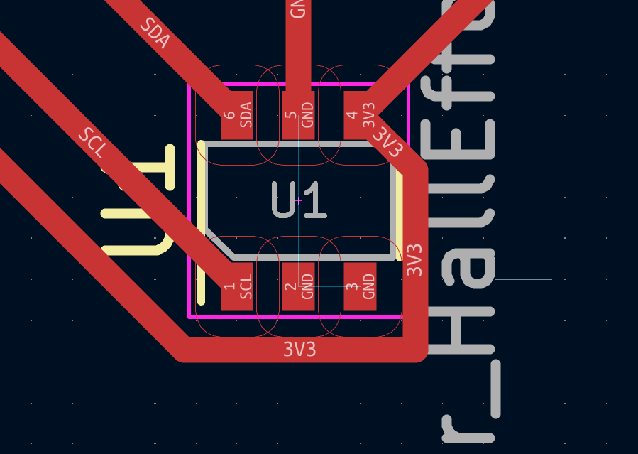
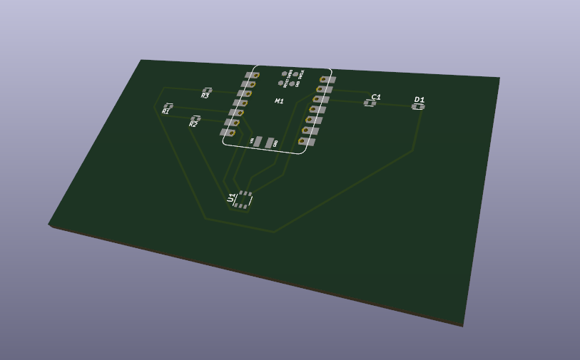
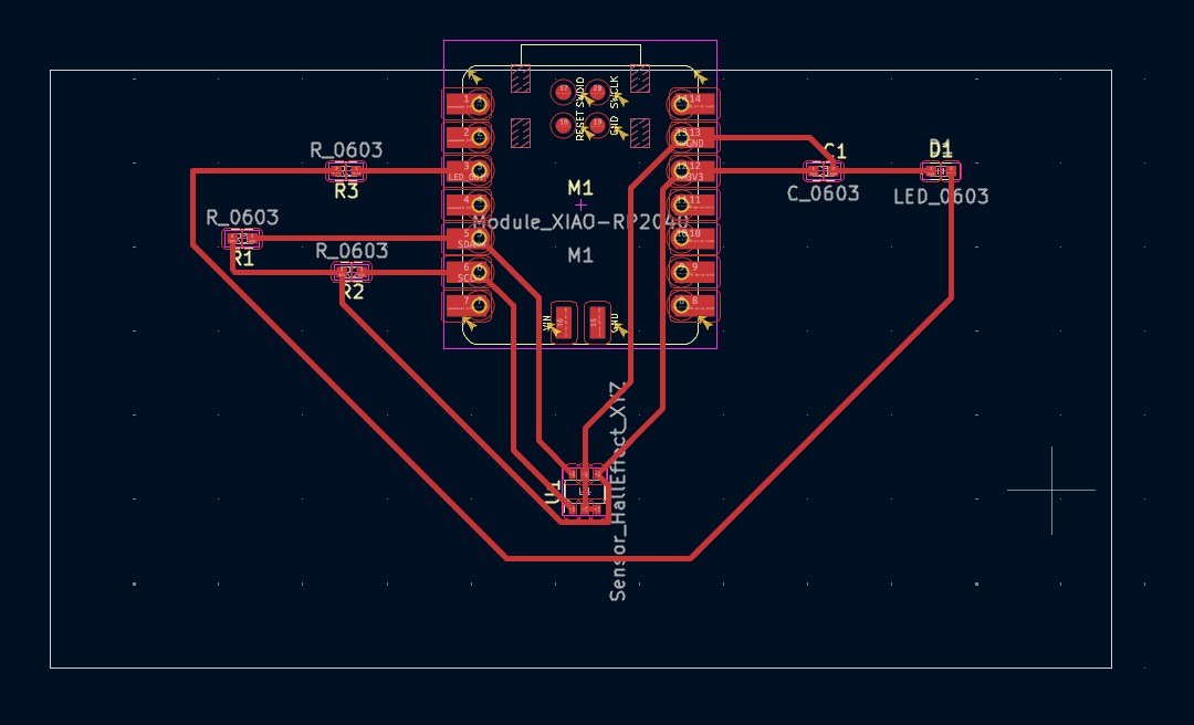
final schematic + pcb
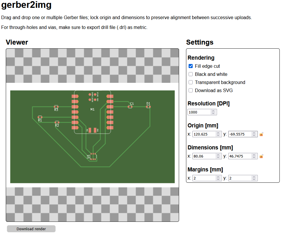
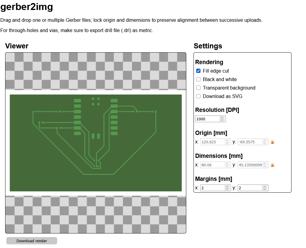
exports → gerber2img preview
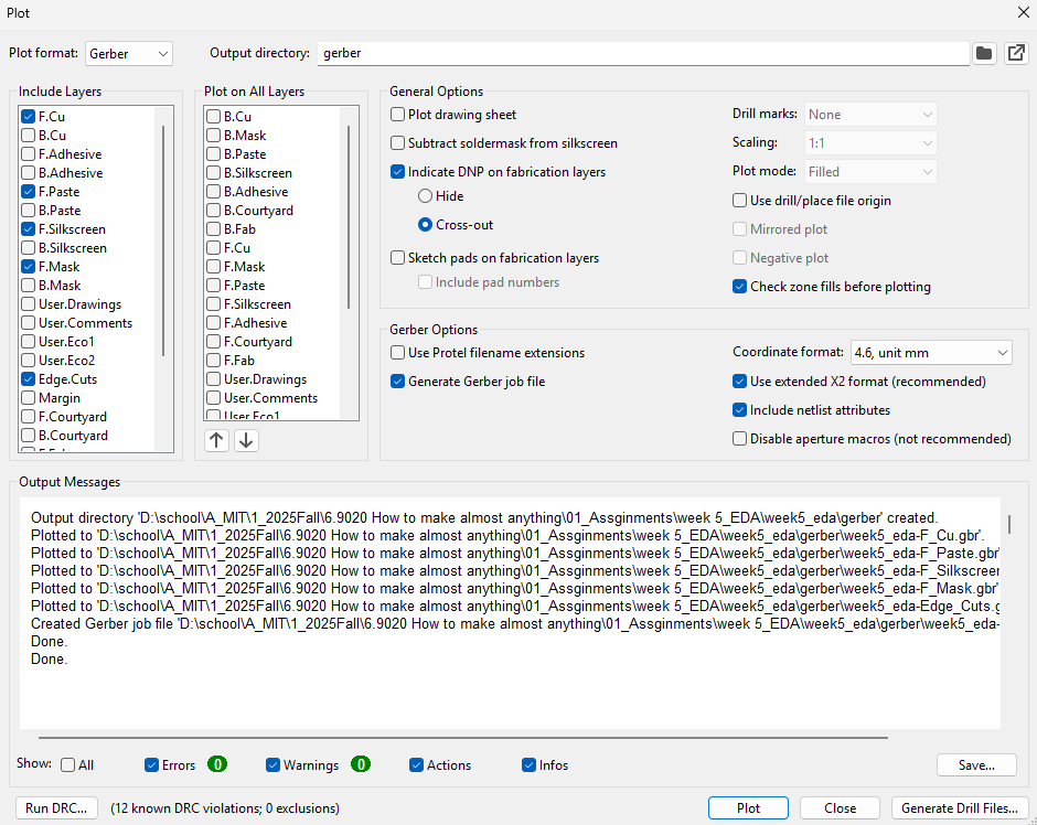
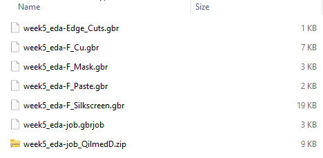
exported the needed layers per recitation, then tossed them into gerber2img to sanity-check.