Group Assignment
Logic Analyzer
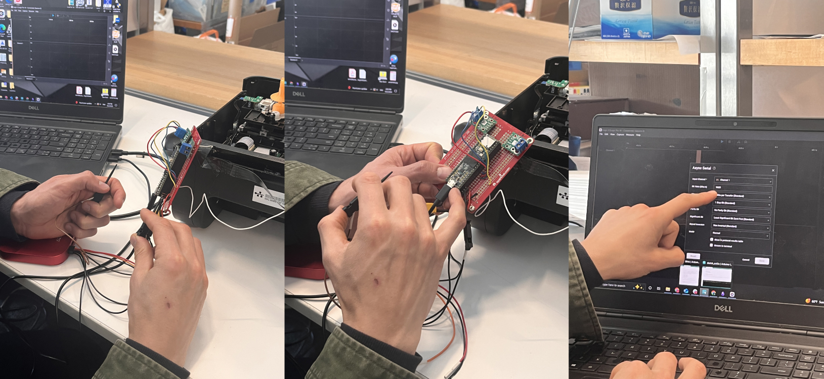
Ben showed us how to use the logic analyzer. connect ground first, then clip probes to the digital pins I want to monitor. Set the sampling rate in the software and start recording. The analyzer captures the high/low transitions over time and can decode protocols like I2C, and SPI. I can zoom in to check timing, confirm if signals are actually being sent, and spot wiring mistakes or protocol errors. Basically, it’s a tool to visualize digital communication and verify whether my microcontroller and peripherals are talking correctly.
Others
- Multimeter: Good for initial checks; it reports an average (or RMS) reading rather than instantaneous voltage. On our model, additional functions are accessed with the yellow button.
- Oscilloscope: Measures voltage over time which is useful for inspecting power rails, data lines, and clock lines. Probe attenuation matters: probes labeled 1x or 10x indicate how the signal is scaled. If you expect 5V but see 0.5V, check the probe attenuation and scope settings.
- Logic Analyzer: Decodes analog voltages into digital logic to visualize signals such as transmit, receive, and clock. I can zoom in to check timing, confirm if signals are actually being sent, and spot wiring mistakes or protocol errors.
PCB Design
Connecting Everything
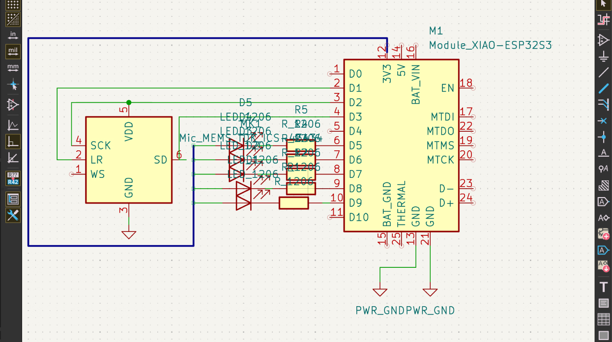
For my final project, I’m building an AI “rock” device along with a base deck for interaction. To begin this system, I designed the PCB for the rock itself. Using KiCad for the first time was overwhelming—so many components, footprints, and symbols—but the core process is simply placing parts, assigning correct footprints, and routing connections cleanly.
For this device, I used the Xiao ESP32‑S3, an I2S microphone, and three LEDs to visualize system status: (1) microcontroller powered, (2) microphone active, and (3) microphone receiving audio data.
Reading the Datasheet
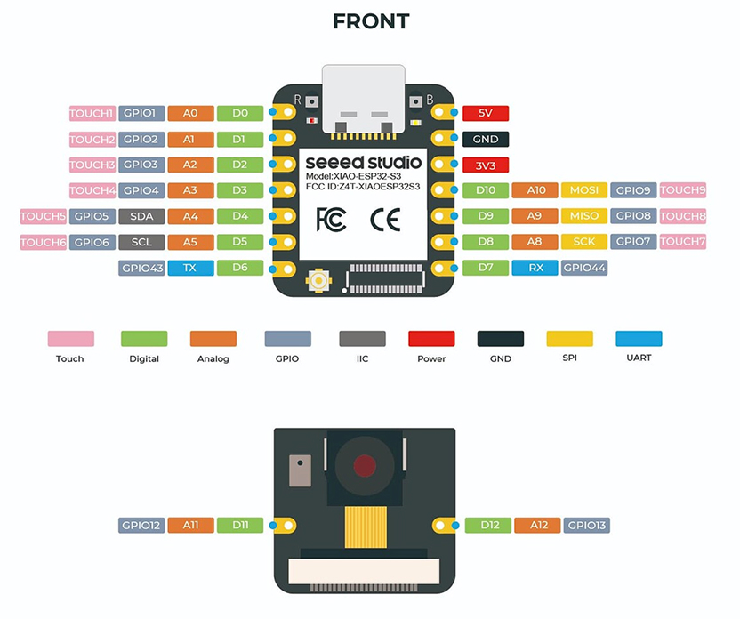
To wire the components correctly, I referenced the ESP32‑S3 documentation. It’s essential to understand where the GND, power pins, and GPIO pins are located. Reading the microcontroller datasheet is key to deciding which MCU is suitable for a design and how each peripheral should be connected.
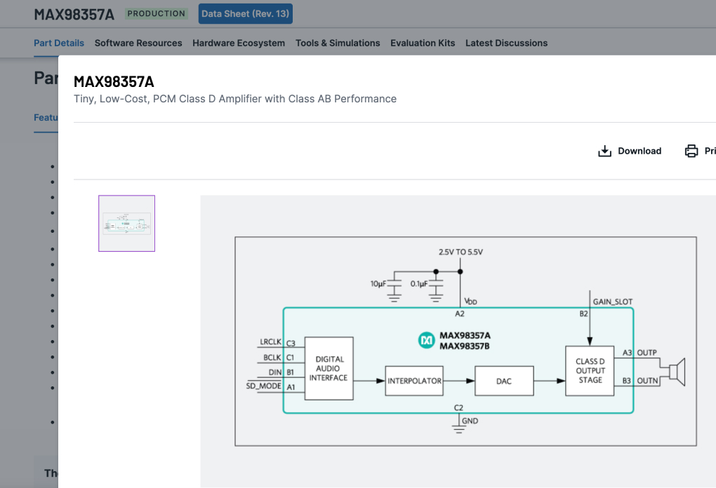
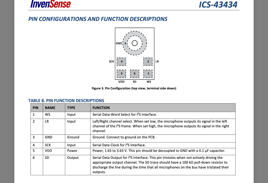
For the ICS‑43434 microphone, I checked the datasheet to confirm its power requirements, the correct I2S pin mapping, and the orientation of the acoustic port. This helped ensure the microphone would receive clean power and data signals.
PCB Design
Connecting Everything
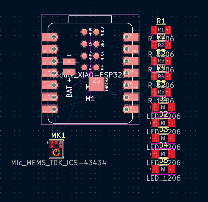
After clicking “Update PCB,” KiCad automatically transfers all schematic components and their footprints to the layout—magic! From there, the main task is routing the traces according to the design rules.
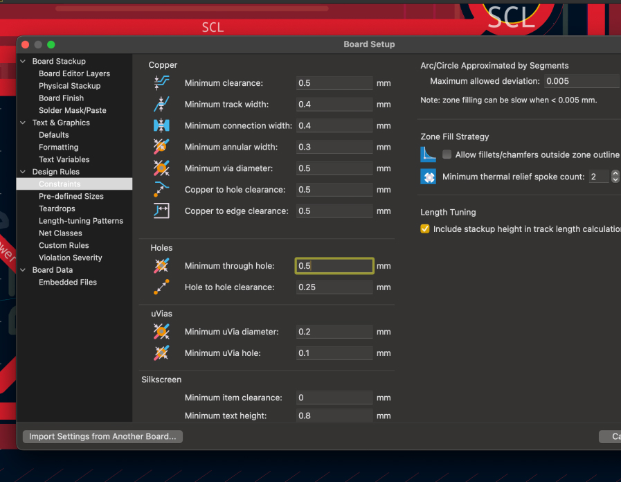
These are the design rules I used to ensure the trace width and spacing match the milling machine’s endmill size, preventing traces from tearing or merging during fabrication.
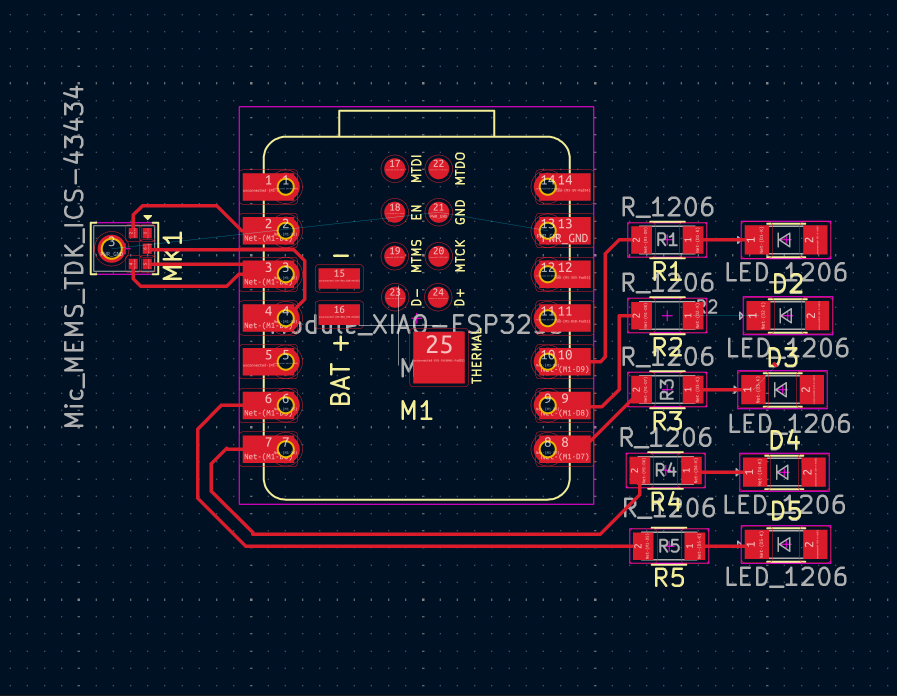
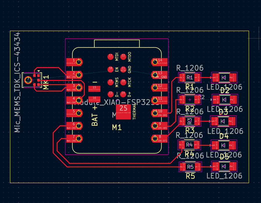
For routing the PCB, Quentin suggested:
- it's good to make wires not to bend 90 degrees and 45 degrees are good.
- We should choose the 0.4mm track width, not the default 0.2mm track width.
- I pressed the design rule checker at the end to see the error and warnings of my design.
3D
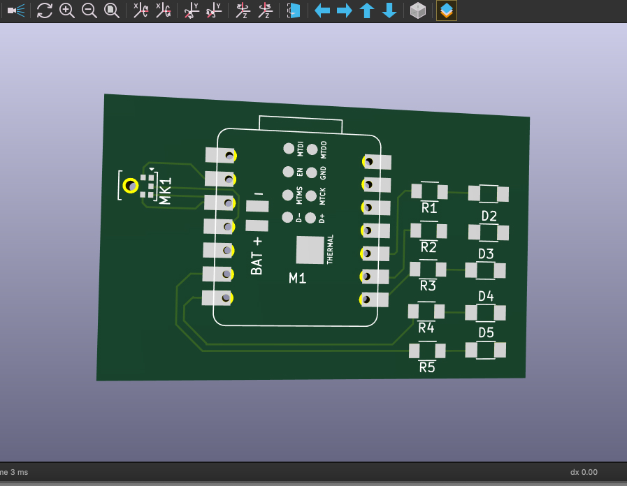
Once the design rule check showed no errors, I used KiCad’s 3D viewer to inspect the board, confirm component orientation, and make sure the overall layout looked clean.
Appendix
Learning from Failures
- When you start the PCB design, first set up the design rules to meet the correct setting that can be used for your milling machine setting.
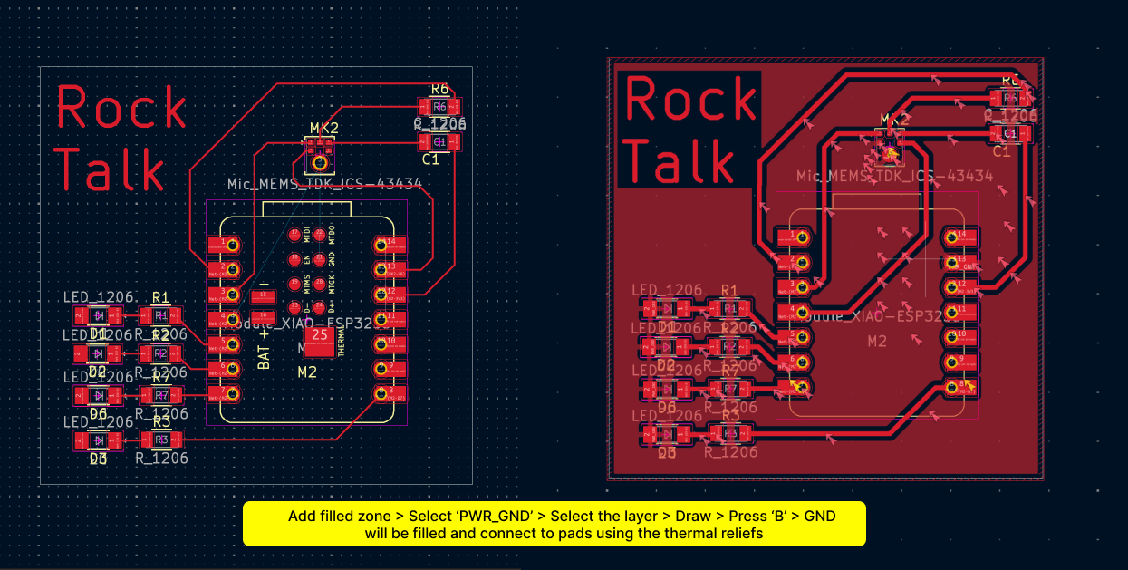
- For GND connections, you don’t need to manually route every trace! I didn’t know this at first and struggled to connect all the LED grounds. Instead, KiCad’s “Add Filled Zone” feature automatically connects all GND pads to a copper pour, simplifying routing and improving board stability.
