
Introduction
This week is focused on Electronic Design Automation (EDA) and Printed Circuit Boards (PCBs). The individual assignment is to use an EDA tool to design an embedded microcontroller system using components from the lab inventory, while ensuring compliance with design rules for fabrication. In the group assignment, we explored the lab’s test and measurement equipment to observe and analyze the behavior of embedded microcontrollers in action.
Group Assignment
Learning to use a Multimeter
As part of the group assignment, we were introduced to key test and measurement instruments used to analyze the operation of a microcontroller circuit board. Our main focus was the multimeter - learning its functions, settings, and safe handling. We used it to measure voltage, current, and resistance across different components, gaining hands-on experience in circuit diagnostics.
We practiced on Gert’s HTMAA final project board, which provided a tangible example of how power is distributed and how current flows through an embedded system.
Notes & Best Practices for Electronics Design
I attended Quentin’s open hours to get a deeper understanding of PCB design workflows in KiCad. Below are my key takeaways and best practices for future projects:
- Software: Use KiCad, the recommended EDA tool (free, open source, cross-platform). It includes separate programs for schematic capture and PCB layout and requires symbol libraries and correct footprint assignments. Alternative: Eagle (within Fusion 360).
- Libraries: Add the Fab Academy KiCad library to access all in-inventory components used in the class.
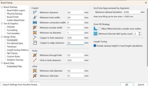
- Design Rules: Set minimum clearance to 0.4 mm (matching the milling bit diameter). Avoid tighter gaps - these can merge during milling.
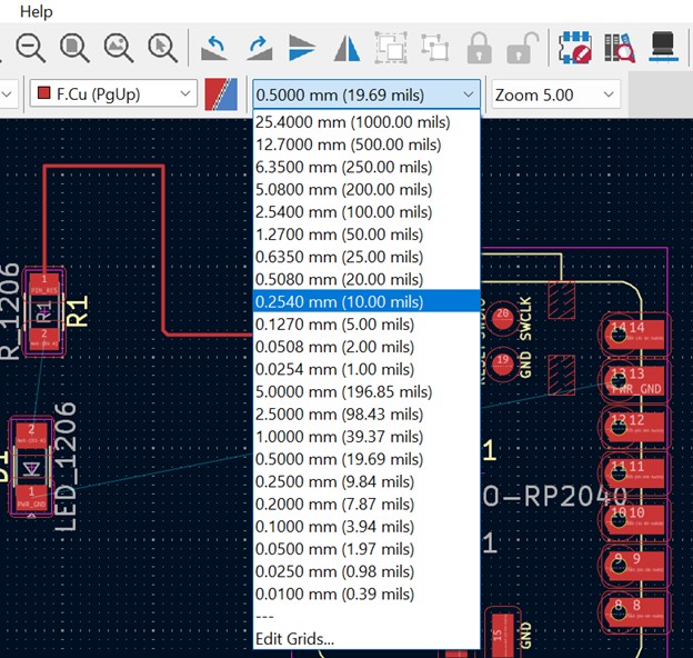
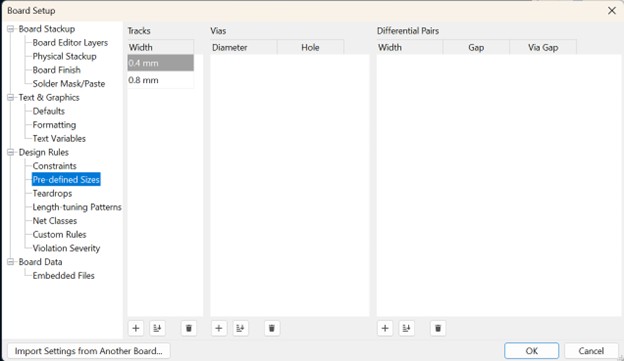
- Track & Grid Settings: Define trace width presets at 0.4 mm and 0.8 mm for easy selection. Use a 10 mil grid, working in multiples for alignment.
- Routing & Placement: Keep parts oriented to allow simple, direct connections and short return paths. Avoid routing too close to board corners to prevent shorts. Plan routes so traces don’t block access to important pads or pins.
- Grounding Strategy: Use a central ground spine when branching ground connections. Prefer a solid backside ground plane and drop vias where necessary.
- Shortcuts:
M= move component;R= rotate while dragging. - Final Checks: Always run the Design Rules Check (DRC) to catch spacing, width, or connection errors before fabrication.
- Simulation Tool: Use Wokwi for quick circuit simulation - helpful for testing logic (note: it doesn’t model analog behavior).
Individual Assignment
Designing a LED Board
Choosing the Board
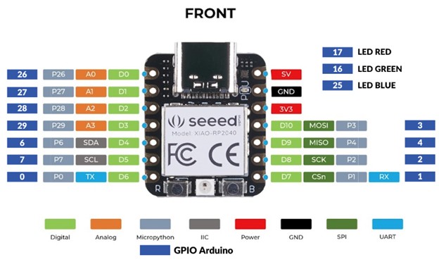
After attending the recitation, I decided to dive right in and start designing my own board. The first step was choosing which microcontroller to base it on. I went with the Seeed Studio XIAO RP2040.
I chose this board because it’s a compact, Arduino-compatible development board built around the Raspberry Pi RP2040 chip. As the smallest member of the Raspberry Pi Pico family, it features a thumb-sized, surface-mount design, making it ideal for compact projects. It’s also compatible with multiple programming languages (C, Python, Go, …) and supported by a wide range of libraries, making it beginner-friendly. Plus... it’s the same board Quentin used during the demo, which clearly made it the safe (and slightly lazy) choice 😄.
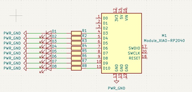
Below are the schematics for the XIAO RP2040 board:
Designing the Schematic
The first step was to draw the circuit schematic. I decided to connect eight LEDs to the board, each through its own resistor. Following Quentin’s guidance, I used 1206 LEDs and 1206 resistors, both standard surface-mount components available in the lab inventory.
I connected the LEDs to digital pins 4 through 11 for two reasons: (1) to achieve visual symmetry on the board (four LEDs on each side), and (2) to keep the analog pins free in case I want to add sensors or other components later.
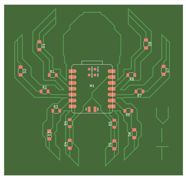
Laying Out the PCB
Next, I moved to the PCB editor and arranged the resistors and LEDs symmetrically across the board. It was finally time to put my consulting skills to good use—all those hours spent aligning and centering PowerPoint boxes definitely paid off when positioning components on the PCB 😄.
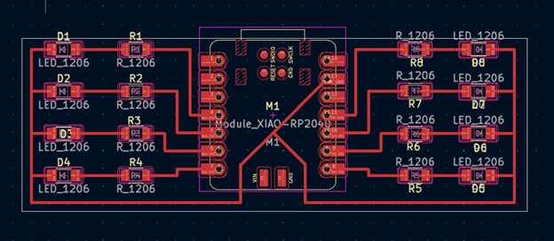
Once the layout looked clean, I connected each LED–resistor pair to its respective pin and added a central ground spine along the back side. After running the Design Rule Check (DRC), I was happy to see it report no errors - a small but satisfying milestone.
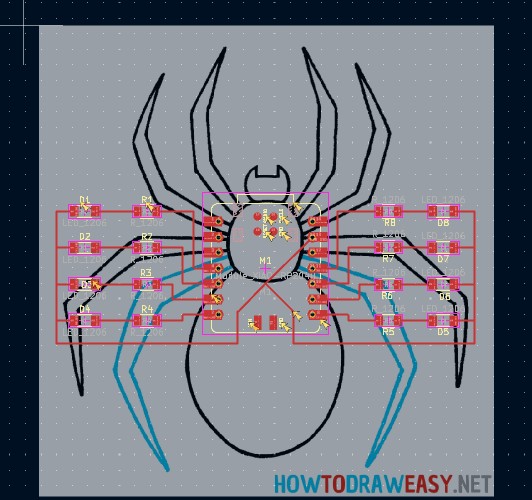
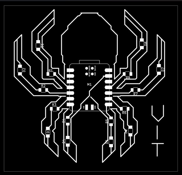
Turning the Circuit into a Spider
When I looked at the layout, I couldn’t help but notice something: the eight LED–resistor pairs looked a lot like a spider’s legs. So I thought: why not lean into it? 🕷️ I uploaded a spider image as a background reference to guide the design and began rearranging the components accordingly.
This time, I added a perimeter trace acting as a ground ring, connecting all the pins around the board. By duplicating and mirroring the wiring symmetrically, the design gradually took shape: a balanced electronic spider—elegant and (possibly?) functional at the same time.
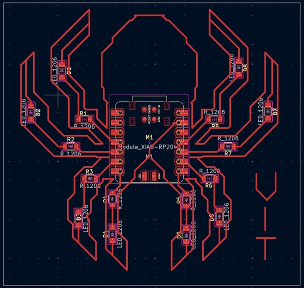
⬇️ Download: Spider Board (ZIP)
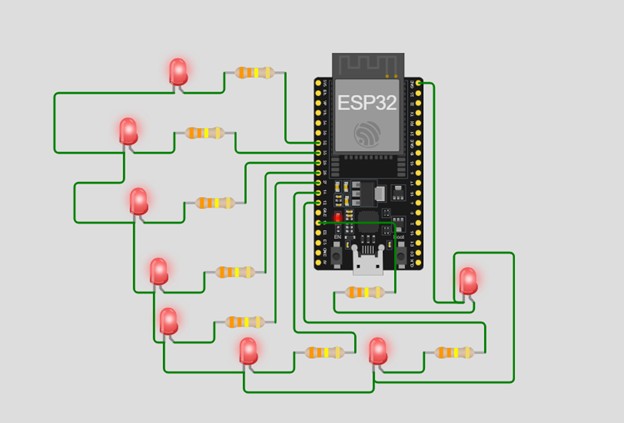
Simulating the Board
To validate my circuit before fabrication, I replicated the board in Wokwi for simulation. Since the platform doesn’t currently support the XIAO RP2040, I used an ESP32 as a substitute. I created eight identical branches with the connection:
ESP32 GPIO → Resistor → LED → GND.
I lkearned it’s important to wire the LEDs correctly, connecting the anode (the long leg) to the resistor and the cathode (short leg) to ground, not the other way around. I selected GPIO pins 13, 12, 14, 27, 26, 25, 33, and 32, which are all safe for output operations on the ESP32.
Once the schematic was complete, I asked ChatGPT to generate a simple program that would make the LEDs blink sequentially, followed by a few collective blinks. The simulation worked, all eight LEDs blinked in the intended pattern.
Code Example
Final Project
Please note that Electronics Design has been part also of my final project. It is well documented in my final project page.