Electronics Design
Group Assignment
1. I worked with my group to use an oscilloscope and a multimeter.
Working with several students from the Architecture section, we explored the use of an oscilloscope (Fig. 1A). During this process we used a wave generator to establish a frequency that we could then visualize on the oscilloscope. We adjusted the amplitude of the wave and and noted the corresponding change.

Fig. 1A. Using the oscilloscope.
We also tested the resistance of a resistor using a multimeter (Fig. 1B). We also used it to check the power of the multimeter itself, discovering that it operates with 5V.

Fig. 1B. Using the multimeter.
There were a lot of students involved in the group assignment this week!
Individual Assignment

Fig. 2A. First iteration of the circuit diagram. (1LED, 1Btn)
For the individual assignment, I decided to design a circuit board with 2LEDs and 2buttons.
Watching EDA tutorials, I familiarized myself with the electronics design capabilities of Fusion 360 and made the first iteration of the circuit diagram (Fig. 2A).
It is an absolute first time I am using Fusion 360, but the recitation session helped a ton to nativate the workspace. In this initial design has one LED and a botton based on the tutorial.

Fig. 2B Helpful tools from the Toolbar
While drawing out the schematic design, I found the tools above to be the most of what I needed to draw and connect the parts.

Fig. 2C. First iteration of the PCB layout.
This is how the PCB layout initially looks. The routes are yet to be connected and the optimal location of the parts are to be decided.(Fig. 2C).
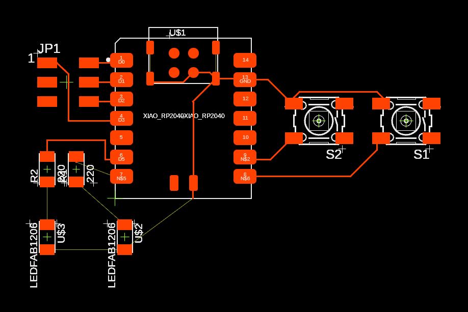
Fig. 2D. Circuit diagram in-progress
In the figure above, (Fig. 2D), I went back to the schematic design and added additional LED and a button.
At somepoint, I had 5 LED located and distributed througout the board, but that just felt like a good way to increase a change to make errors and soldering issues in the future,
so I decided to be ambitious with my design in a minimal way possible.

Final Schematic Design
This is the final schematic design.

Fig. 2E. Another iteration of the circuit diagram.
This is another iteration which took a lot of relocating and re-routing of the parts to eventually make the PCB board space to be compact.

Fig. 2F. Final design.
The image above (Fig. 2F) is the finalized circuit diagram with the boundary of the PCB board having been trimmed and defined further.
I think the routes and the parts can be even more compact, but I thought a little more spacious layout can make it less challenging when it comes to the soldering stage.
For the boundary of the board, I filled the corners to make the remaining outer area of the board more compact and to avoid sharp edges.

Fig. 2G. Image of PCB layout.
This is the image of the PCB layout after being exported into a PNG format.
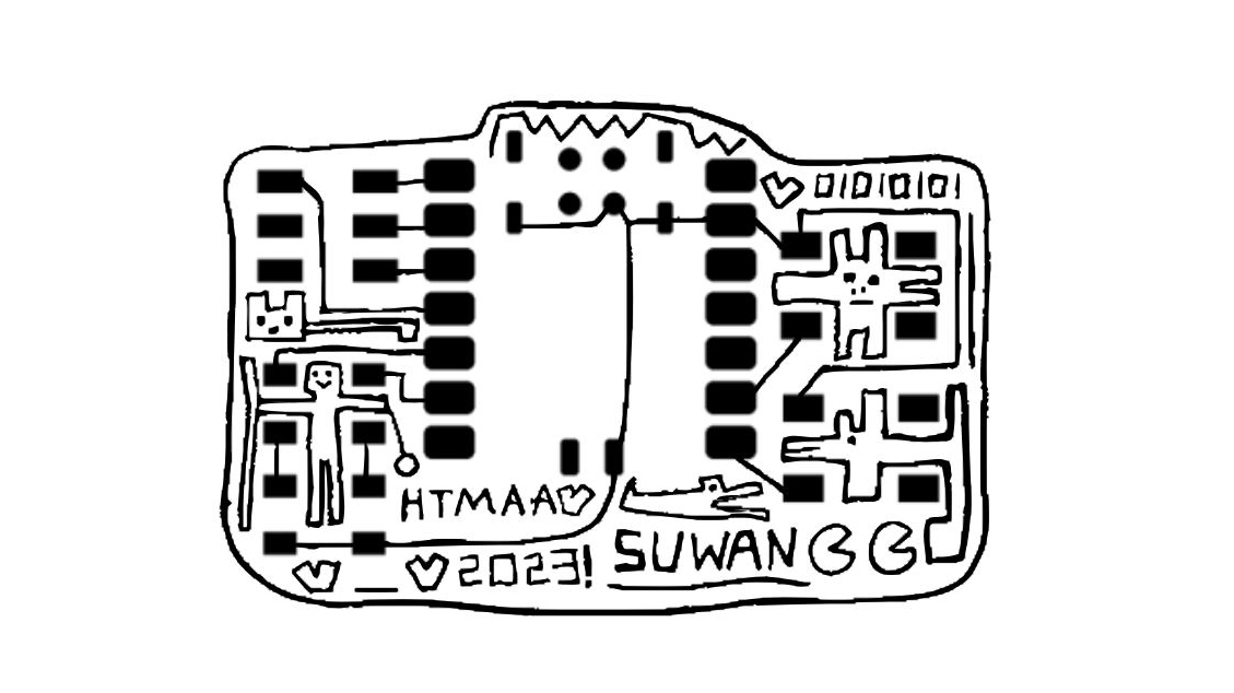
Fig. 2H Attempt to customize
The figure above is my attempt to customize the board. I drew the lines via my drawing tablet. I just wanted to put some cute line elements. The resolution is very bad at the moment.