PCB Design, Fabrication, & Assembly
The goal of this assignment was to fabricate (mill) and assemble (stuff) a PCB. A PCB or printed circuit board is used to mechanically support and electrically connect electronic components using conductive pathways, tracks or signal traces etched from copper sheets laminated onto a non-conductive substrate. This is something I've never done - thank you to the TAs and classmates for their help. More photos: Flickr Set
I had the good fortune of debugging my board in the High/Low Tech group where I learned about soft circuits and the amazing resource How To Get What You Want. This gives me hope for my final project. Other Final Project related links - Final Project Preparation.
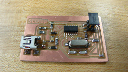
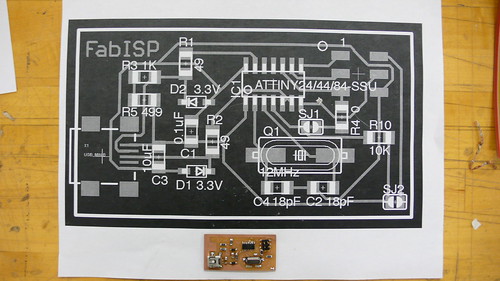
At Long Last
A working FABisp or SEDisp in this case.
|
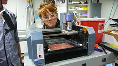
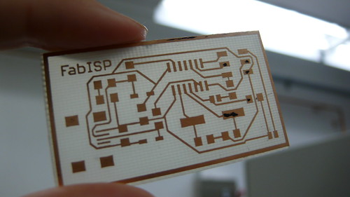
Milling
In this case we were given a PCB design and used a Modela or David Carr's Mantis milling machine to trace the design onto a copper sheet. We were helped along by CAMIT.
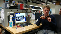 |  |
| David Carr in action | PCB - 2" x 1" |
 |
 |
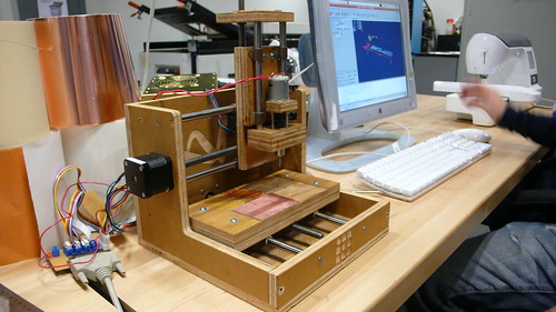
| $100 Mantis Milling Machine | The Modela | 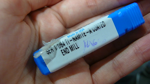 |
| Joint Size Testing | Mantis at work |
 |
|
| Mantis Interface | Mantis Interface |
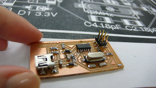
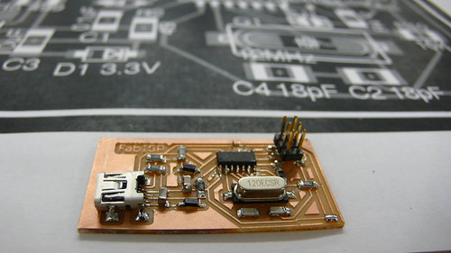
Stuffing
Was more difficult than expected. I'd never soldered anything so tiny.
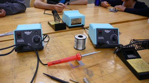 |  |
| Weller soldering irons | Stuffed |
 |
 |
| Stuffed | Stuffed | 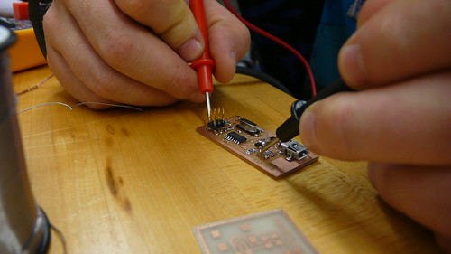 |
 |
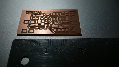
| Testing | Etched Board |
|
|
|
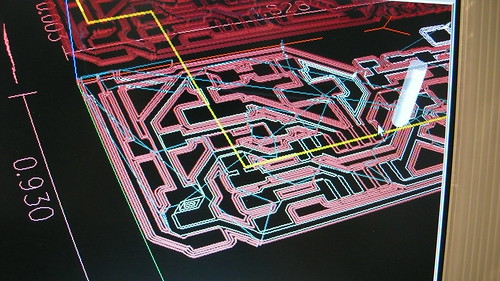
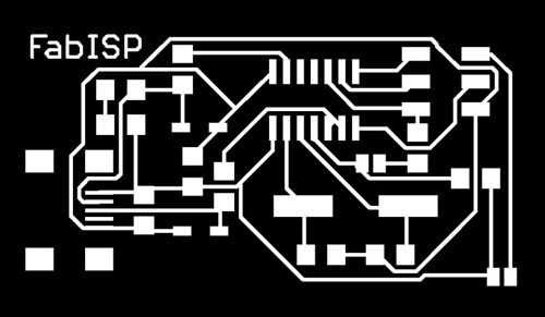
Given PCB Design
|
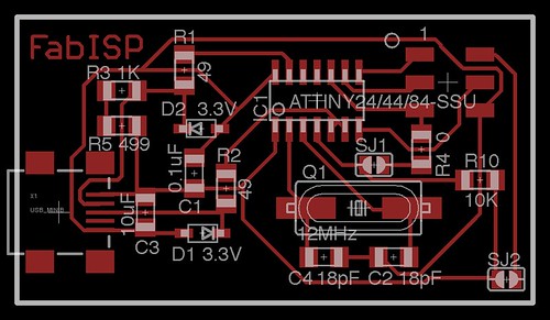 |
PNG of PCB to Mill |
 |