Week 5: Electronics Design
12 Oct 2016 · 4 min readThis week’s assignment was to redesign the echo hello-world board and fabricate the modified version.
I decided to use the EAGLE PCB Design software, because it seemed like an industrial-strength tool for PCB design. Also, I had used it once before (just for making schematics, though), so I was more familiar with it than I was with other tools!
Schematic
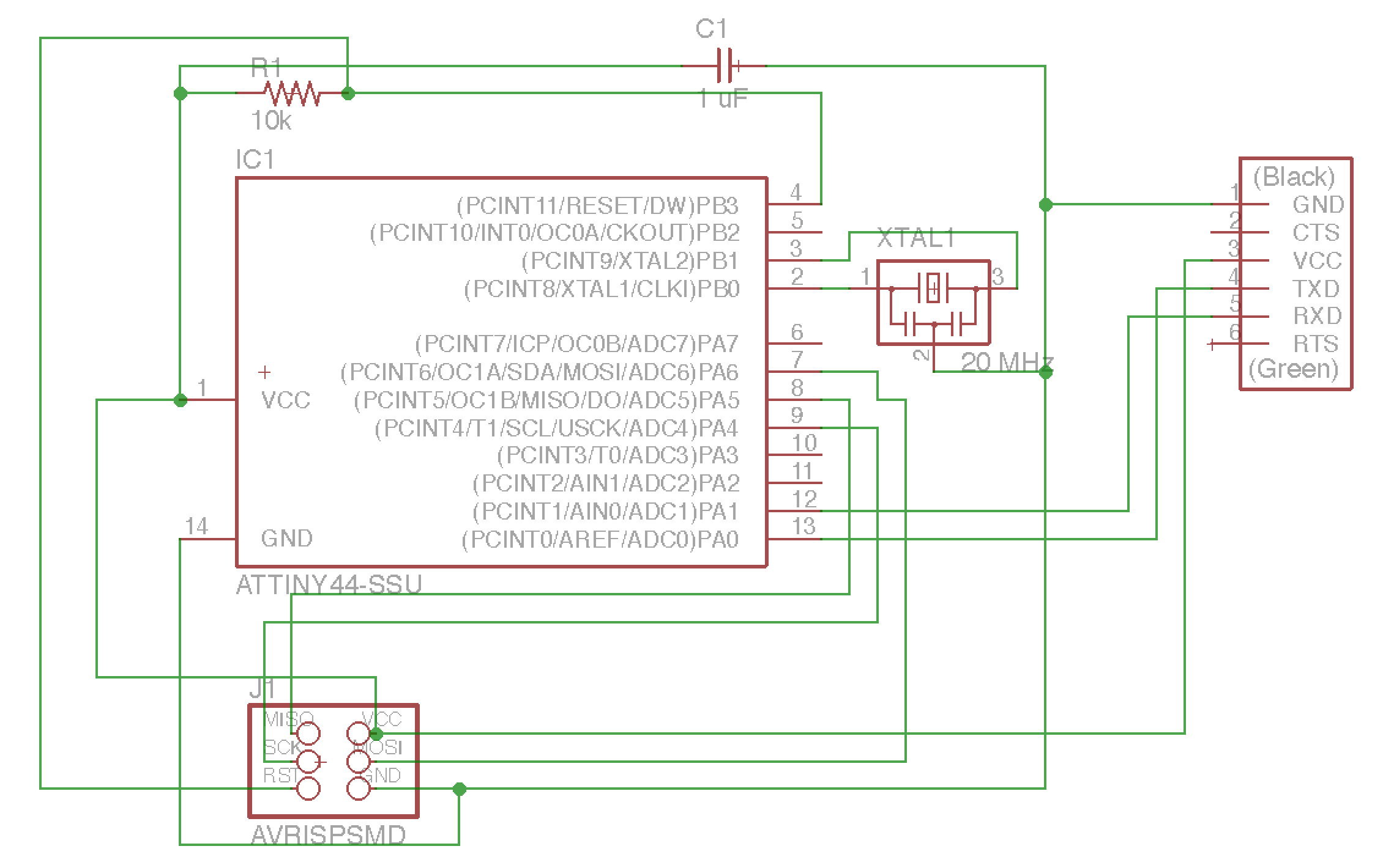
I started out replicating the schematics of the echo hello-world board:
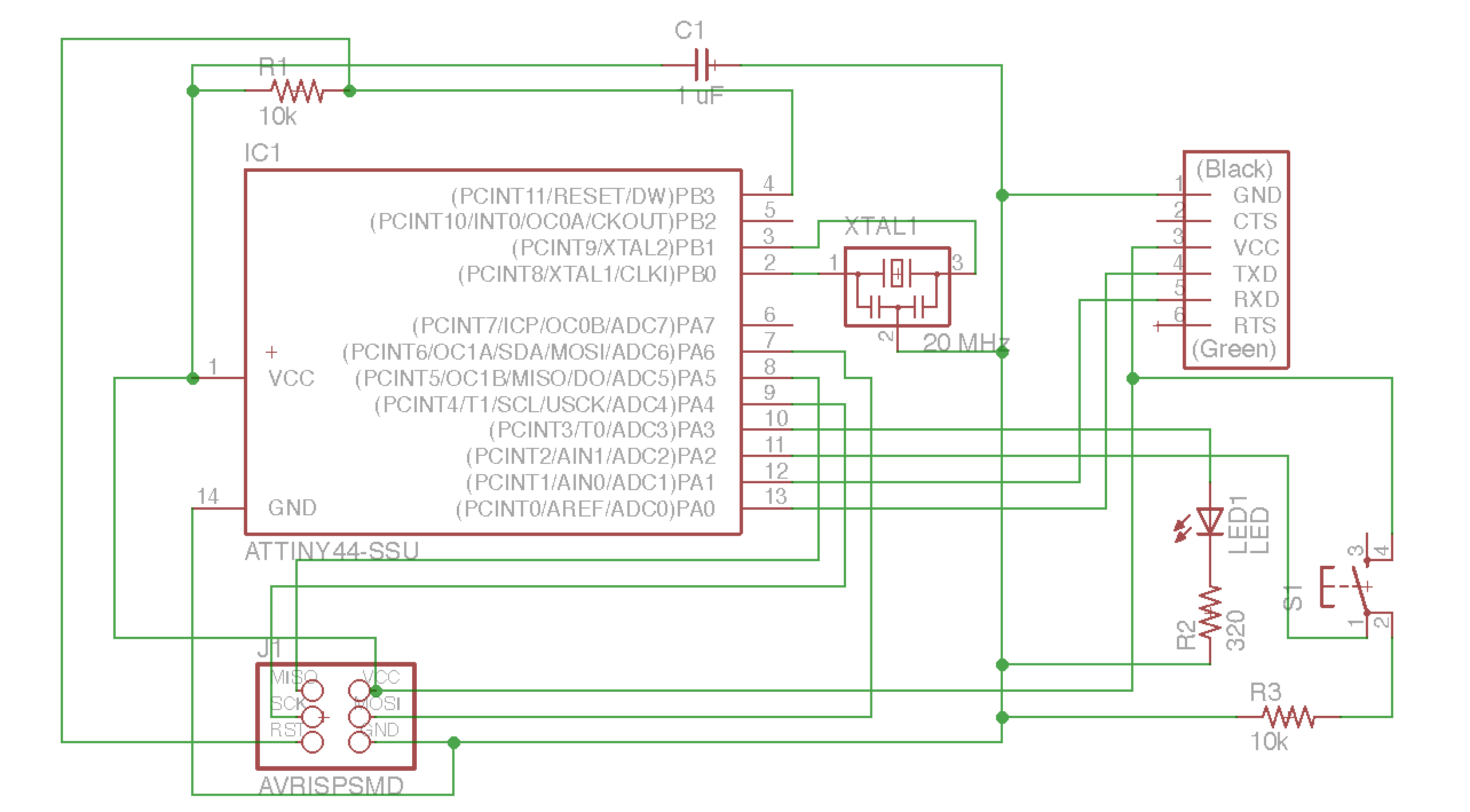
I added a button and an LED to the design.
When adding the LED, I made sure to put it in series with a current-limiting resistor. To estimate the resistance required, I considered using a blue LED, which has a voltage drop of about 3.4 volts. With a desired current of 5 mA through the LED, a (5 V - 3.4 V)/(5 mA) = 320 Ohm resistor is required.
When adding the button, I decided to use a pull-down resistor configuration. Essentially, the microcontroller’s input should always be driven high or low, and using a pull-up or pull-down resistor with the button is a way to achieve that. I chose to use a 10k Ohm resistor.
Here is the final schematic with the button and LED added:
Board Layout
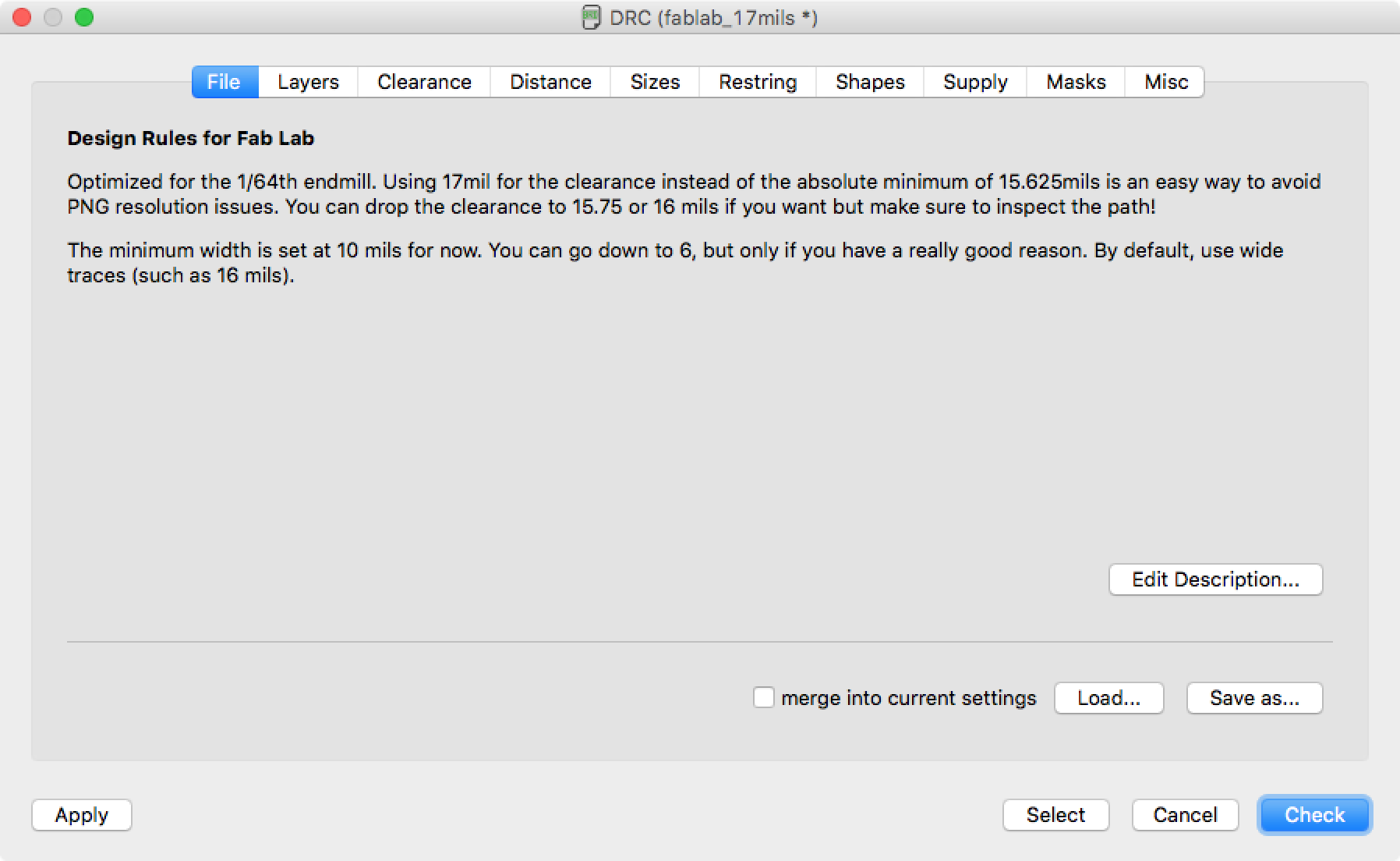
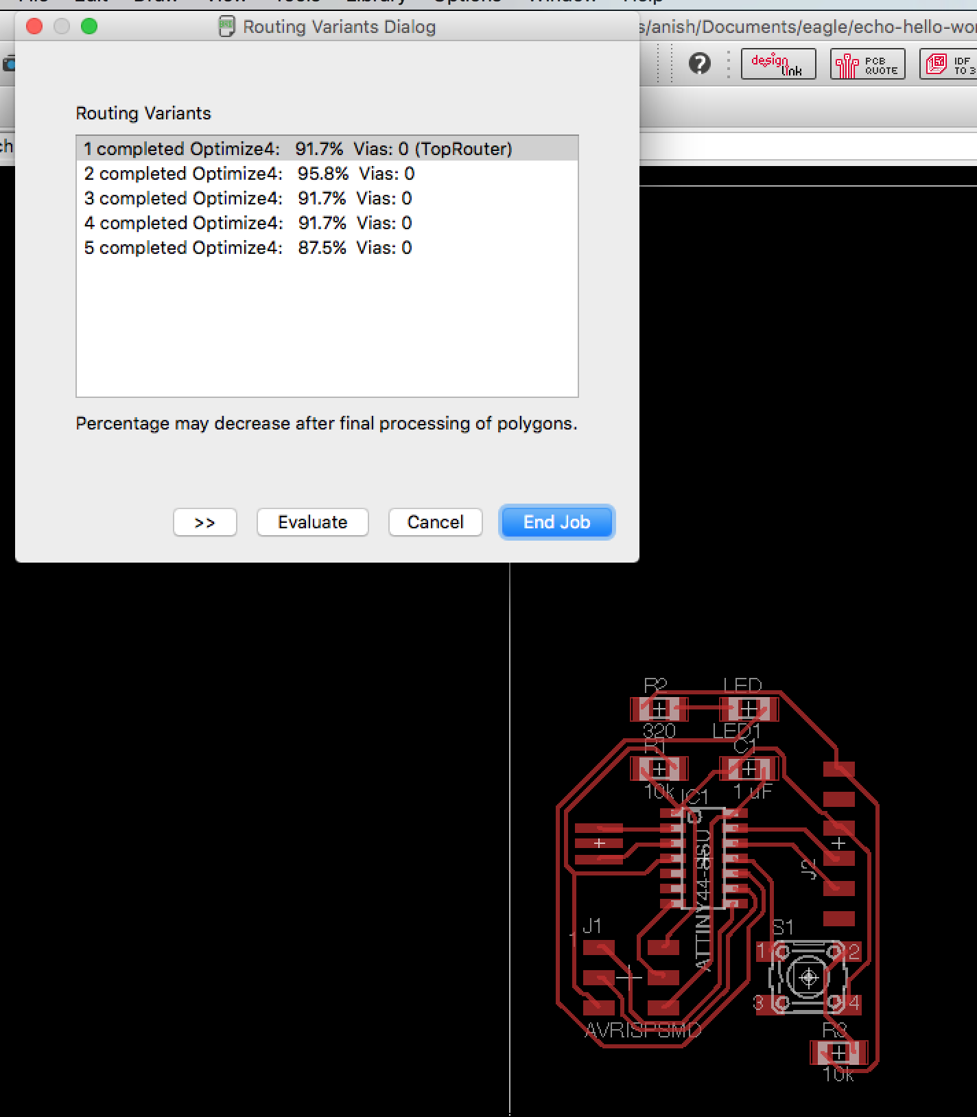
After designing the schematic, I did the PCB layout and routing. The first step was to import the Fab Lab PCB design rules into EAGLE so that the design would be optimized for the 1/64” endmill used on the SRM-20 (which would be used later for production):
Next, I laid out the components on the PCB and tried to use EAGLE’s autorouter, which attempts to automatically figure out how to wire everything together while respecting the design rules and avoiding things like crossing wires. By default, the autorouter uses 2 layers, but I disabled the 2nd layer, which forced the autorouter to route for a single layer PCB. In my first try, the autorouter couldn’t route all the wires (none of the routing variants are at 100%):
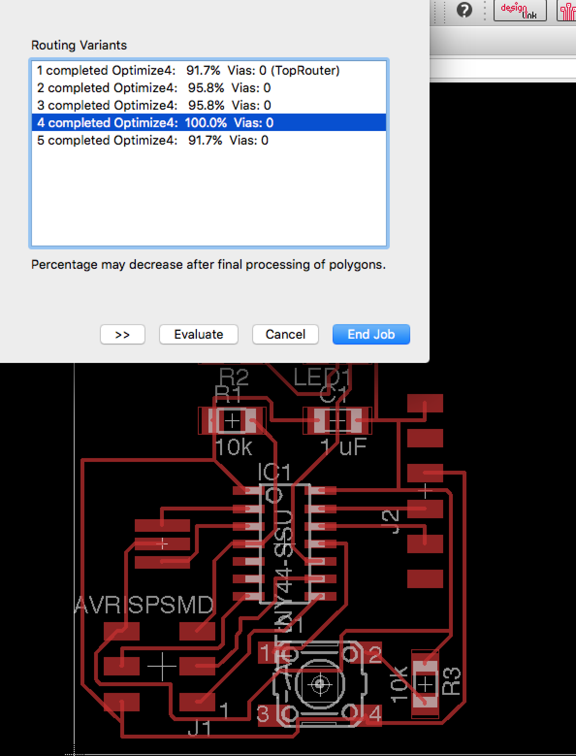
After moving and rotating parts to try to improve the design, I tried the autorouter again, and it managed to route all the traces:
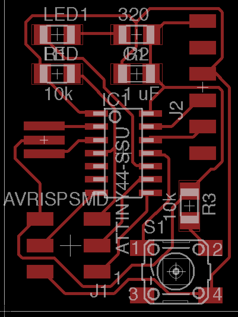
Now that I knew that routing was possible and that the autorouter could find a valid routing, I played around with the design to try to get it to be a little more compact. Here are the final results:
Exporting
Now that I had a PCB layout I was happy with, I needed to figure out how to export it so that I could mill a PCB. Eagle can export PNG images of PCBs — I just needed to disable all the other layers in “View > Layer Settings” so that I could get a clean image.
I exported an image at 1270 ppi, imported it into Photoshop, cropped it slightly, and made a 64 pixel border for the PCB outline. Here is the final result:
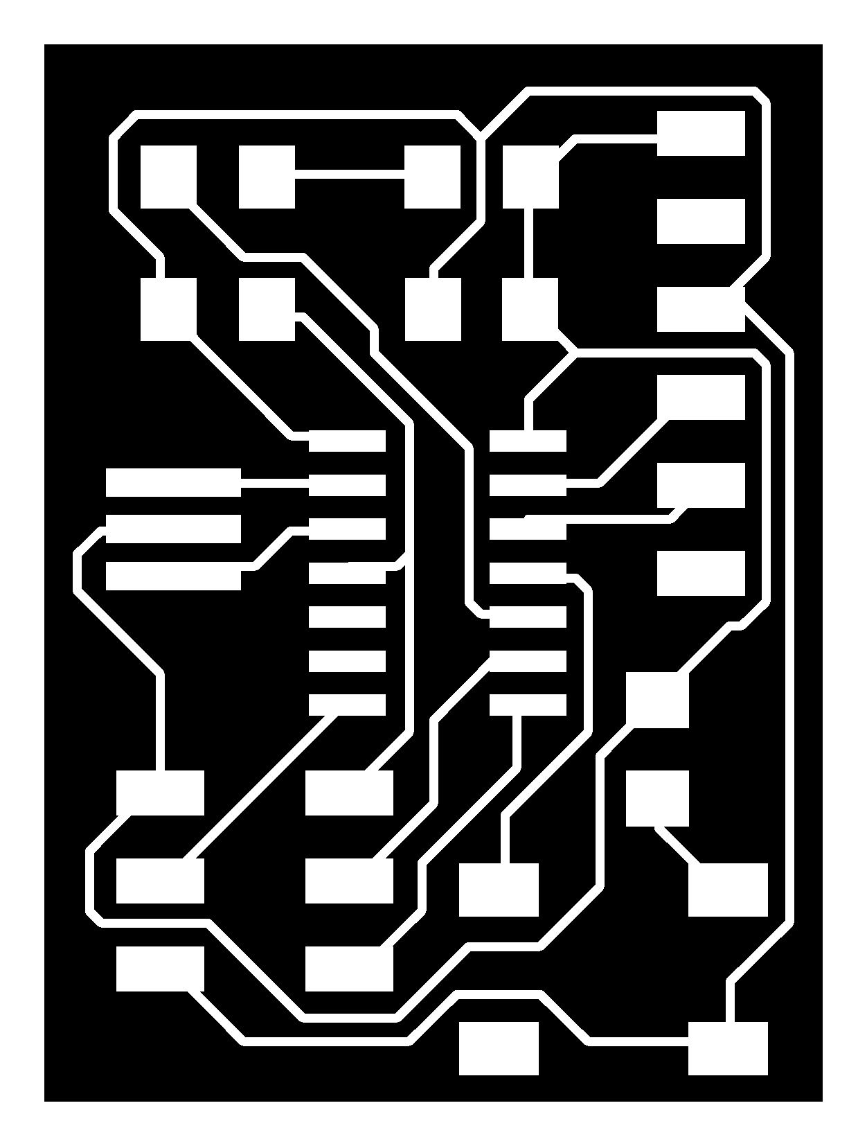
The traces can be found here, and the outline can be found here.
Fabrication
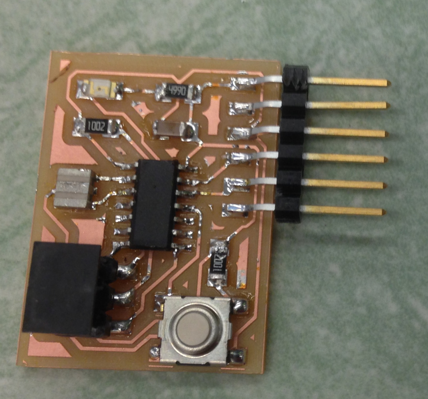
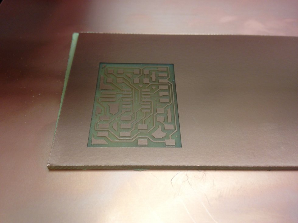
Using the same methods used in week 3, I fabricated a PCB. Here’s the freshly milled board, about to be removed from the SRM-20:
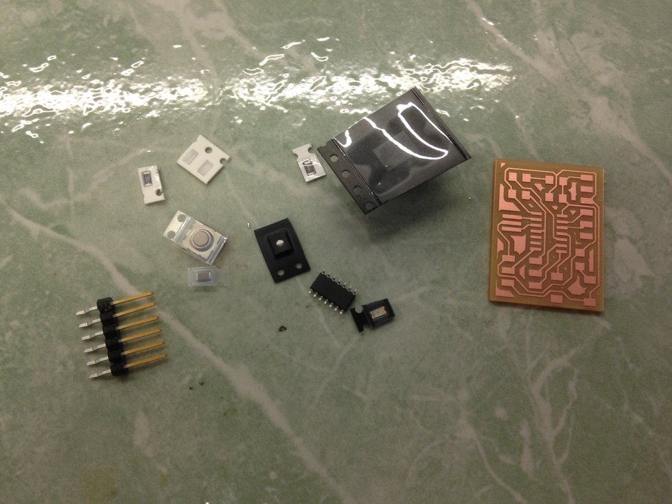
Choosing components for the board, I made some slight modifications to the design:
- Chose to use an orange LED, which has a voltage drop of about 2.1 volts
- Chose to use a 499 Ohm resistor with the orange LED for a current of (5 V - 2.1 V)/(499 Ohm) = 5.8 mA through the LED
Here is the PCB and components, ready to be soldered:
Here’s the final result: