Final Project Ideas
This is a tracking page, so it captures my ideas, documents the progress on the final project while at the same time capturign changes and transitions in my ideas.Initial thoughts
A key idea that has intrigued me for a while is that given matter, energy and a set of instructions, we can create anything from anything (within second law limits. Additive manufacturing is one step in this direction - we take some raw materials (usually limited to 2 or 3 materials ahving fairly similar physical properties) and energy, usually in ther form of thermal (FDM) or electro-magnetic (SLA) and coupled with a set of instructions (G-code) we can create complex objects.
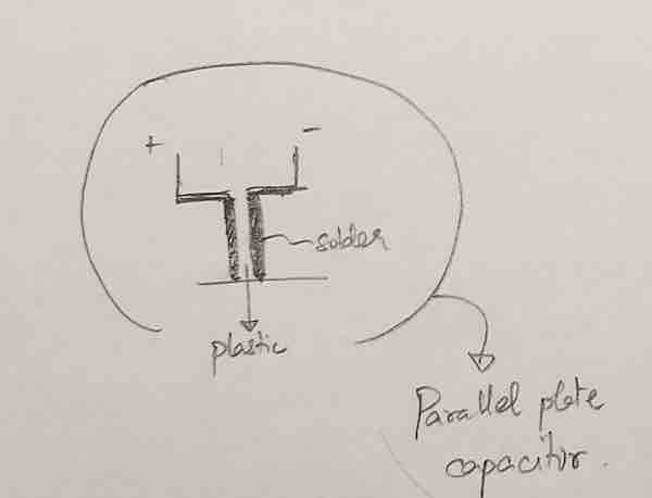
Along similar lines, I would like to create a system that can take materials with varying physical properties (as a starting point) and create integrated parts. My preliminary idea for this is to use insulators and conductors - plastic and metal, that can be used to create circuits and maybe even simple components like a parallel plate capacitor, such as the one sketched here.
Integrated circuitry within typical thermo-plastic prints
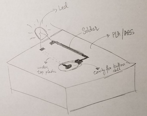
In this example I've sketched how one might design a battery holder along with integrated wires or connections that can be secured to a LED to form a simple circuit.
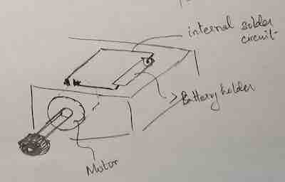
In the below picture a similar circuit with a AAA battery and a simple motor is sketched
Update
So as I was going through the past few weekly assignments, I realised I could better scope my project and make something that is usable (as opposed to just the drive mechnaism for the above idea)
In the electronics production week I realised that it can be challenging to get smooth, shiny solder joints, so I started wondering if I could desing a smart solder pen that
integrates the temprature sensing and the actual deposition of the solder at the deisred location.
 The adjacent image here shows what this might look like. You have a solder pen that has the solder wire inside it, a positioning "claw" at the tip that helps hold on to
components and temperature sensors at the tip that can sense when the pads/component connections are heated enough to avoid cold joints.
The adjacent image here shows what this might look like. You have a solder pen that has the solder wire inside it, a positioning "claw" at the tip that helps hold on to
components and temperature sensors at the tip that can sense when the pads/component connections are heated enough to avoid cold joints.
 In the close up drawing you can see how the claw holds on to the component and when the temperature is right signals the user to press a button which the forces the solder wire thorugh to be deposited to form the joint. A second beep or flash signals the user to remove the soldering pen.
 The drive mechancism can be pretty straightforward as shown in the drawing. It could be a simple gear that is driven by a motor and a tensioning bearing.
The solder wire would be squished between the two such that it can be pused by the motor driven gear.
The drive mechancism can be pretty straightforward as shown in the drawing. It could be a simple gear that is driven by a motor and a tensioning bearing.
The solder wire would be squished between the two such that it can be pused by the motor driven gear.
Update 2
So I realised I really don't like solder that much, and I like making things that I can use in my day-to-day life, like the cool bookrack or the laptop stand I made.
 So I'm thinking about making a smart watch that I can use, inspired by previous project done in the class.
I really like an "analog" display so I thought it would be cool to use an LED array to show the time (different brightnesses/ or bliking to diffirentiate between the hr, min and s).
I've started practicing/ prototyping as you can see in Week 10. More updates will follow here! Stay tuned!
So I'm thinking about making a smart watch that I can use, inspired by previous project done in the class.
I really like an "analog" display so I thought it would be cool to use an LED array to show the time (different brightnesses/ or bliking to diffirentiate between the hr, min and s).
I've started practicing/ prototyping as you can see in Week 10. More updates will follow here! Stay tuned!
Things I want on my watch...
- Accelrometer
- Bluetooth module
- Temperature sensor
- LED indicators for notifications
- Piezo vibration motor for alerts
- "Analog" watch face using LEDs
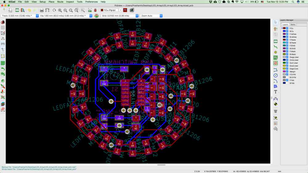
Kicad model
I've started thinknig about the prototype. Hoping to mill out the boards this week.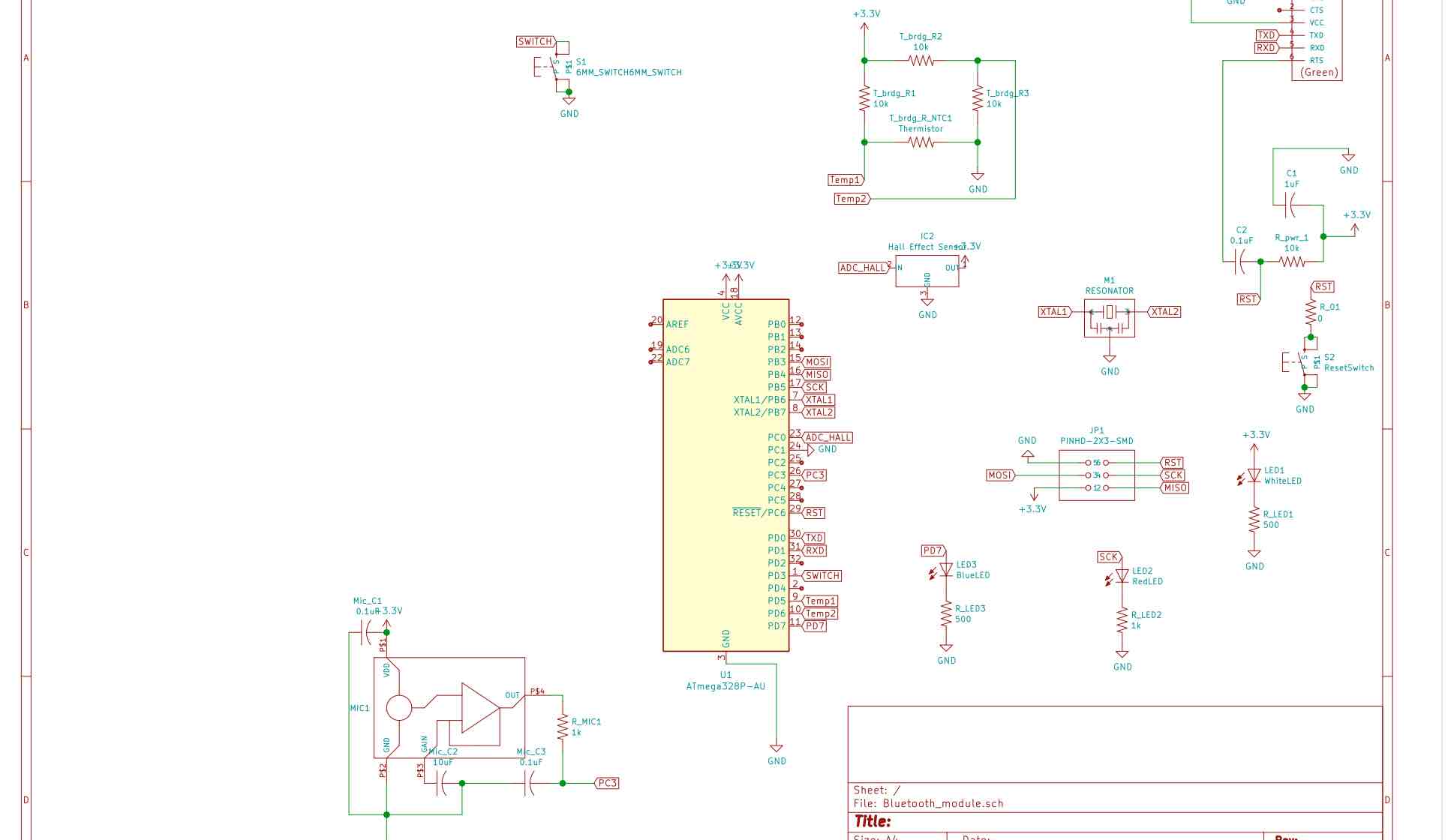
Update: Prototype functional board with sensors, LEDs and Bluetooth communication
Last week I managed to mill a prototype board that has sensors and wireless communication capability. After some "RTFM" issues (See here). I was able to talk to the bluetooth module. I'm currently working on talking to the ATmega328p on my board via bluetooth.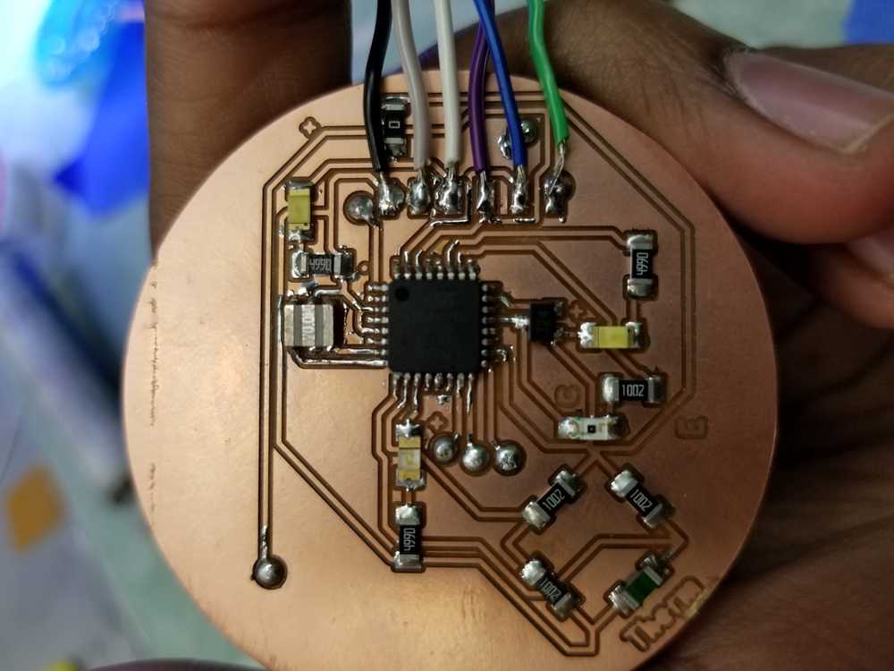
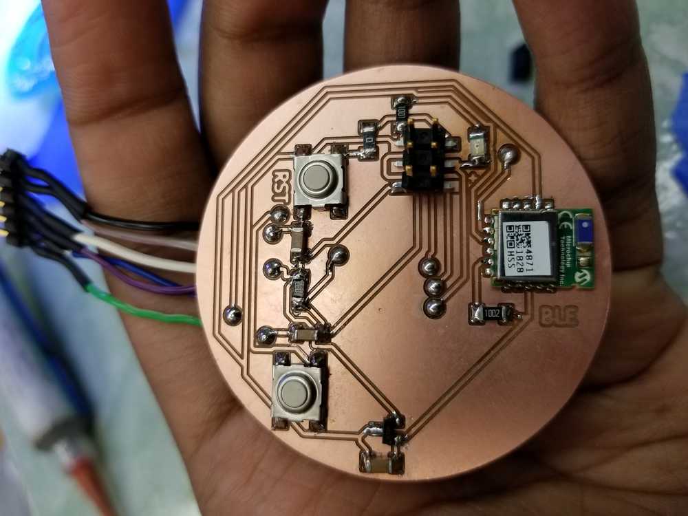
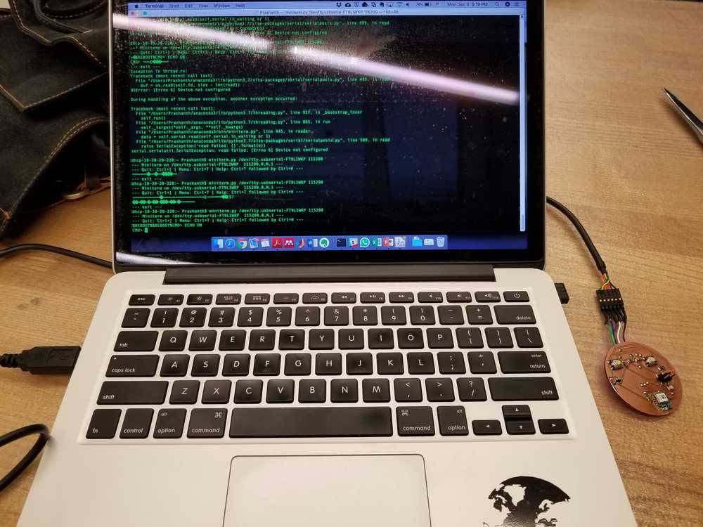 I was able to get the hall effect, temerature and proximity sensor working on the board. Also managed to test the button to be able to control the LED. These checks were mainly to ensure that I was reading the datasheet for the ATMega328p correctly and able to program it based on exapmles that I have successfully worked on in the past few weeks.
 The next step is to learn how to do SPI communication for the addressable DotStar APA102 LEDs.
Adventures with an engraving bit
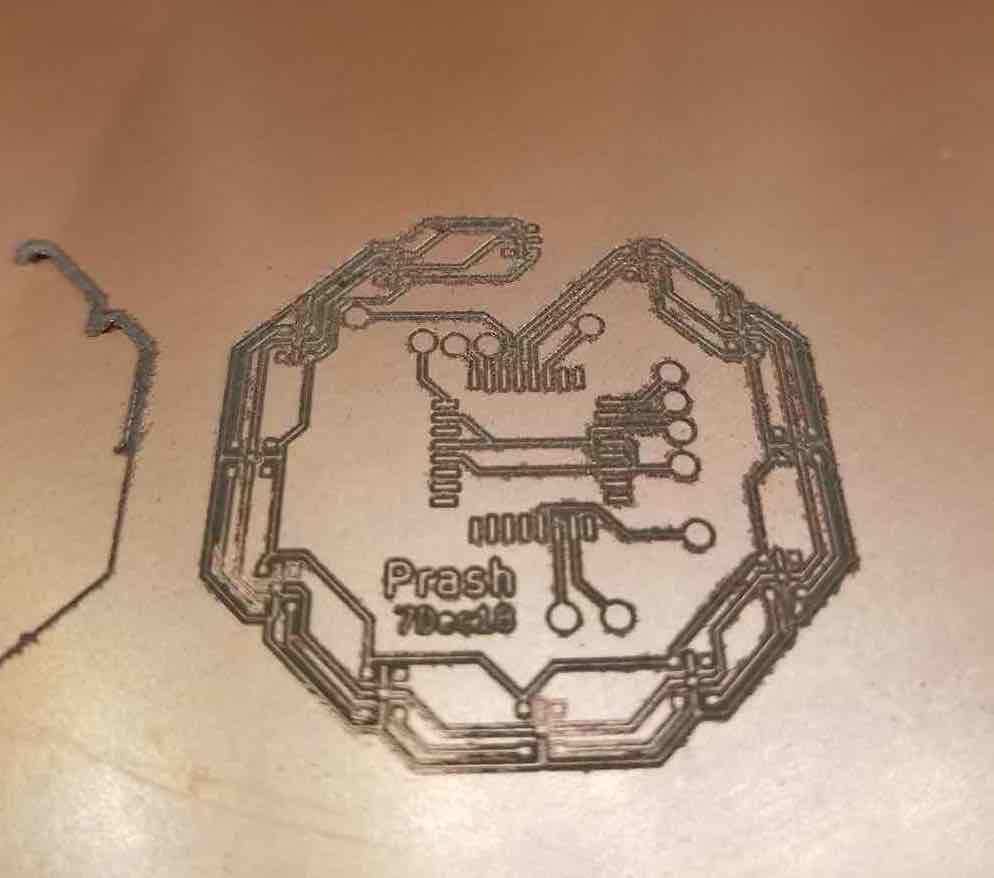
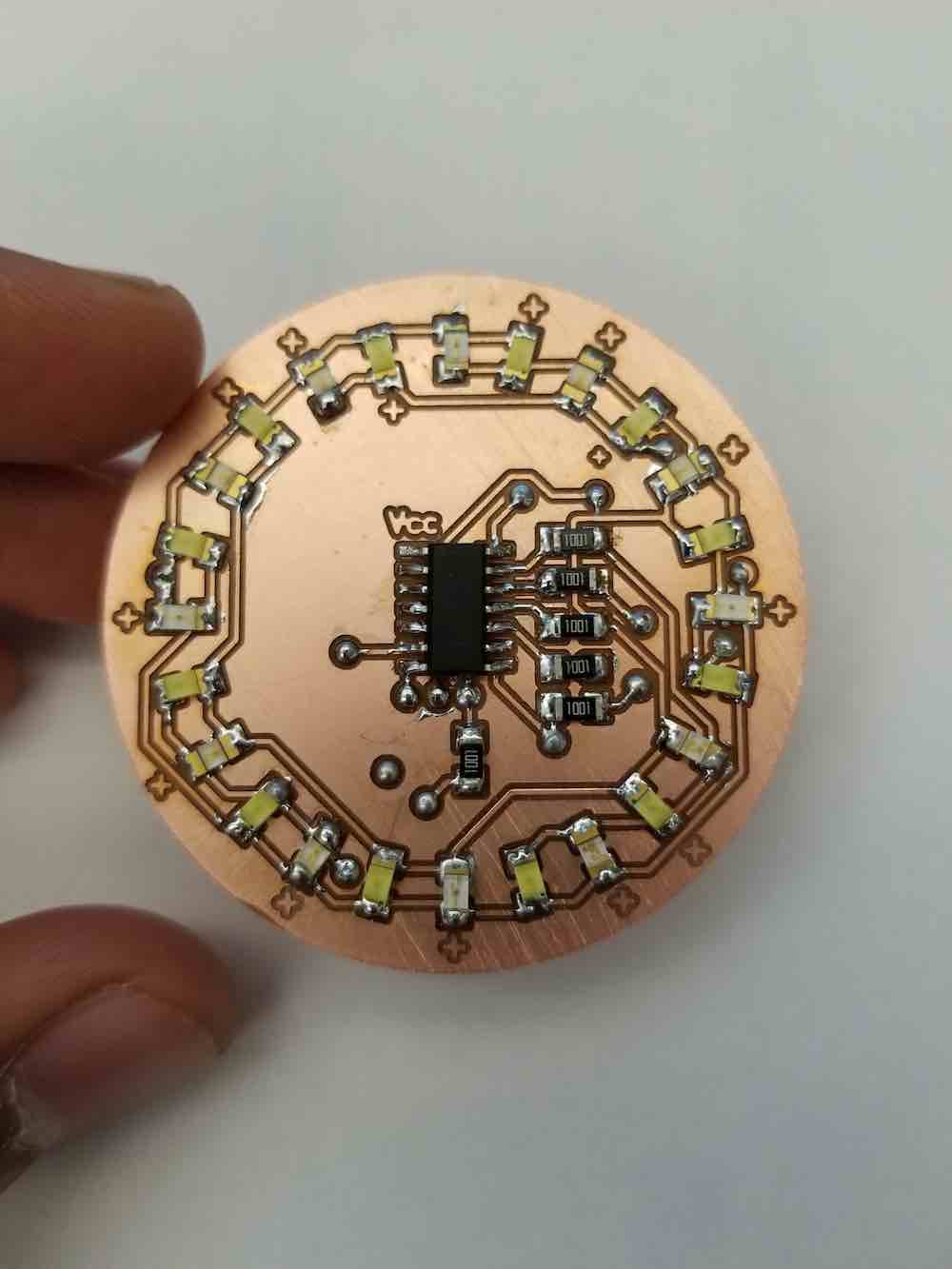
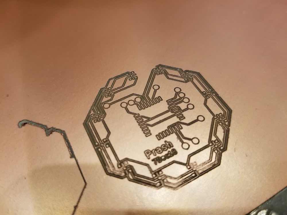
Now that I had the LEDs ready, I decided to mill out a new protorype board with the 12 LEDs and the required components to test.
The pads on the APA102 are really small, so I decided to use the engraving bit in the EECS lab. Now the thing about these engraving bits (cheap ones) is that they are (a) super inconsistent in that tool 1 would behave significantly differnetly than tool 2 and (b) they are super sensitive to variations in the working surface. That is to say if the working surface is uneven, which is almost always the case when we fixture the double sided board with sticky tape on both sides, the tool may work nicely on some parts and do a terrible job on others, since the Z height varies
.
These tools will break if you look at them too hard (Ben, 2018)
Naturally these were super annoying to work with. I did multiple tries, with varying depth of cut, spindle speeds, feed rates etc but the results were far from satsifactory.
I then decided to go back to kicad and modify the pads until the just touched the leads on the DotStar LEDs. I pushed it to the point where I could just use the 1/64th bit (which works beautifully).
Tried it now and it still required a little post processing with a knife to cut away some traces, but wayyyyy better than the engraving mill.
Mini-test board for the LEDs and SPI
 Since the main board that I had designed had a lot of parts it was taking a while to mill. I decided to make a "break-out" board with just my LEDs and some bluetooth capability to test those two out before investing the time in making a far more complex board.
This board confirmed that I could:
- use the 1/64" bit to mill the APA102 Pads
- solder the LEDs using the heatgun
- use SPI to control the LED brightness and colours
- contorl them via bluetooth connection from by phone
I thought I had soldered them properly but truns out there were some solder bridges so I had to remove and re-do the LEDs. I suspect this is due to the small pads and poor contact with the leads, so I know that I need to probably change the design file a little more.
Programing the addressable LEDs
 Now that I had the board ready, it was time to dive into programing the addressable LEDs using what is called Serial Peripheral Interface (SPI).
The main way this works is by using a data line and a clock line to tell the components which data bits are valid. This is usually done at the rising or falling edge of the clock signal.
Now that I had the board ready, it was time to dive into programing the addressable LEDs using what is called Serial Peripheral Interface (SPI).
The main way this works is by using a data line and a clock line to tell the components which data bits are valid. This is usually done at the rising or falling edge of the clock signal.
While trying to learn how to do this, I found a useful explanation on SparkFun. The image here does a good job of showing what the whole SPI jazz is about.
The tutorial by Tom here was really useful in getting started. However there seem to be a few errors/bugs on there that I fixed.

APA102 addressable LED SPI protocol
The protocol for the LEDs are as follows:
- A start frame of 4 bytes of '0'
- A frame of 4 bytes for each LED to set brightness and colour
- An end frame of 4 bytes of '1'
Pseudo-code for setting colors and brightness
for (1 to 4) send(0 byte);
set data to 1 or 0 based on LED value required;
set clock high;
//here is where the data is registered
//on the rising edge of the clock
wait;
set clock low;
for (1 to 4) send(1 byte);
A simple write function
void Write (uint8_t val) {
  int i=0x80;//0x80=0b10000000 used to set 1 bit at a time from MSB to LSB
  while (i) {
    if (!(val & i)) PORTA &= ~(1 << PA7);  // set Data low
    else PORTA |= (1 << PA7);              // set Data high

    PORTB |= 1 << PB2;               // set Clk high
    i = i >> 1;//move the 1 bit so next iteration reads the next bit in val
    _delay_ms(10);
    PORTB &= ~(1 << PB2);           // set Clk low
  }
}
Bluetooth
WIP
Watch Body
Here I start designing the packaging:Designing the body in Fusion360
Though my usual go to CAD software has been Solidworks, I decided to use Fusion360 for a more sculptable design which I hear that Fusion is really good at.After a bunch of tutorials online I designed the following watch face: