Week Eight: Embedded Programming
This week I made an oscilloscope with an ATMega328. The scope can measure between -10V and 10V and uses the internal ADC and comparator for triggering. It samples at around 150ksps and sends the data over USB.
ADC
I configured the ADC to operate in free running mode, which means it samples continuously and calls an interrupt when each new sample is ready, which is once every 13.5 ADC clocks. The ADC clock cannot be as fast as the processor clock, so a prescaler is applied. For simplicity, I chose to sample at 8 bits instead of the full 10 bits. At this resolution I found the fastest ADC clock I could use was 4MHz, a clock prescaler of 4. Here is the code that configures the ADC and then functions to start and stop it.
void init_adc()
{
    cbi(ADCSRA, ADEN); // disable adc
    cbi(ADCSRA, ADSC); // stop conversion

    cbi(ADMUX, REFS1); // choose AVcc with external cap
    sbi(ADMUX, REFS0); // for adc voltage reference
    sbi(ADMUX, ADLAR); // left adjust adc readings for 8 bit
    ADMUX |= ( 0 & 0x07 ); // choose analog 0 pin

    sbi(ADCSRA, ADATE); // enable auto trigger of adc
    sbi(ADCSRA, ADIE); // enable adc interrupt

    cbi(ADCSRA, ADPS2); // set prescaler to 4
    sbi(ADCSRA, ADPS1); //
    cbi(ADCSRA, ADPS0); //

    cbi(ADCSRB, ACME); // choose AIN1 for comparator

    cbi(ADCSRB, ADTS2); // choose free running mode
    cbi(ADCSRB, ADTS1); // for auto trigger adc
    cbi(ADCSRB, ADTS0);
}

void start_adc()
{
    sbi( ADCSRA, ADEN );
    sbi( ADCSRA, ADSC );
}

void stop_adc()
{
    cbi( ADCSRA, ADEN );
    cbi( ADCSRA, ADSC );
}
Comparator
Next I set up the analog comparator to provide triggering. The ADC samples continuously into a circular buffer until the comparator output is high, meaning the input signal is above the trigger level. The ADC then fills half the buffer with samples. This way the trigger event is always at the center of the circular buffer. To filter out some noise from the comparator I added a simple filter that requires eight samples in a row above the trigger level for the trigger to engage. I configured the comparator without an interrupt because I just read the comparator value in the ADC interrupt.
void init_comparator(void)
{
    cbi( ACSR, ACD ); // turn on comparator
    cbi( ACSR, ACBG ); // choose digital pin 7 for comparator
    cbi( ACSR, ACIE ); // disable interrupt

    cbi( ACSR, ACIC ); // disable input capture interrupt
}
ADC Interrupt
The ADC interrupt implements a circular buffer of 1024 8-bit samples. At each interrupt it checks if the comparator has detected the input voltage above the trigger level eight consecutive times, then sets the stop_index which the interrupt will freeze itself at when it hits it.
ISR(ADC_vect)
{
    adc_data[adc_counter] = ADCH; // read adc
    if (freeze) {
        freeze = false;
        stop_index = -1;
    } else if (adc_counter == stop_index) {
        freeze = true;
    } else if ( comp == 0 && (ACSR & (1 << ACO)) && stop_index < 0) {
        stop_index = ((adc_counter + (ADC_BUFFER_SIZE >> 1) ) & 0x03FF);
    }
    adc_counter = (( adc_counter + 1 ) & 0x03FF); // increment adc counter
    comp = (comp << 1); // push next comparator value
    comp += (ACSR & (1 << ACO));
}
Trigger Level
Next I made it possible to set the trigger level in software. The ATMega328 does not have a DAC but it does have PWM which can be used to provide a reasonably stable DC output by adding an RC filter. The PWM output has a frequency of 490 Hz so I used a 100 kΩ resistor and 1 uF capacitor which provides reasonable delay and ripple in the mV range. Here is the code to use PWM on PD3. After this init function the duty cycle can be changed by modifying the OCR2B register.
void init_pwm()
{
    setOutput(DDRD, PORTD3);
    sbi(TCCR2A, COM2B1);
    sbi(TCCR2A, WGM20);
    sbi(TCCR2B, CS22);
    OCR2B = 128;
}
Signal Conditioning
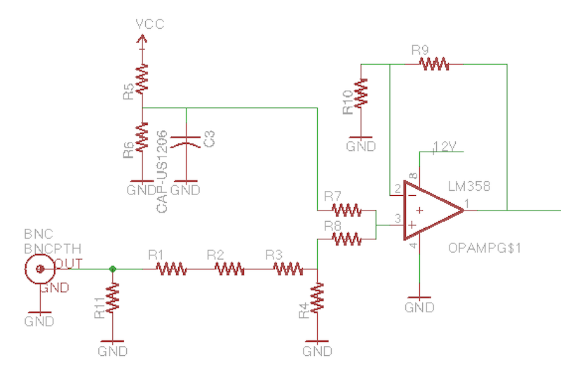
Next I designed a signal conditioning circuit. The ADC measures from 0V to 5V, but I wanted a larger input voltage range. The circuit uses an op-amp to scale and offset the incoming signal from -10V to 10V to 0V to 5V. It does this with a divide by four voltage divider and then a voltage adder with a 2.5V input made by a divide by two divider with 5V. All resistors in the schematic are 10kΩ except for R11 with is 1 MΩ to make the scope appear as a high impedence to whatever circuit it is measuring.
UART
I configured the UART at 115200 baud. Here's the code to initialize it and then functions to send and receive characters.
#define BAUD 115200
#include <util/setbaud.h>

void uart_init() {
    UBRR0H = UBRRH_VALUE;
    UBRR0L = UBRRL_VALUE;

#if USE_2X
    UCSR0A |= _BV(U2X0);
#else
    UCSR0A &= ~(_BV(U2X0));
#endif

    UCSR0C = _BV(UCSZ01) | _BV(UCSZ00); // 8 bit
    UCSR0B = _BV(RXEN0) | _BV(TXEN0); // enable rx and tx
}

void uart_putchar(char c) {
    loop_until_bit_is_set(UCSR0A, UDRE0); // wait until reg empty
    UDR0 = c;
}

char uart_getchar() {
    loop_until_bit_is_set(UCSR0A, RXC0); // wait for byte
    return UDR0;
}
Board
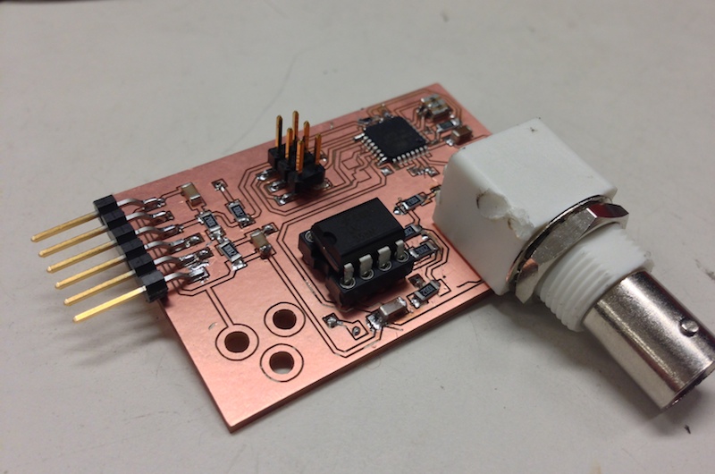
Finally I designed and milled a board for the scope. The board includes the ATMega328 and signal conditioning circuit as well as a BNC connector I got from SparkFun. The board is two sided so I learned how to mill two sided boards. To get the via holes I exported the vias layer from Eagle which contains the via pads. I imported it into an image editor where I used the paint bucket tool to fill the background, and then inverted the image. This left just the via holes in black with a white background, ready for the fab modules. I used 1/32" vias in Eagle to make sure the 1/32" endmill could mill them. After milling the top layer and the via layer, I cut out the board, flipped it over, and placed it in the bottom right hand corner of the hole. I then offset the zero point in the fab module by 1/32" in both axes and milled the bottom traces, remembering to flip the bottom traces image horizontally so it lined up.
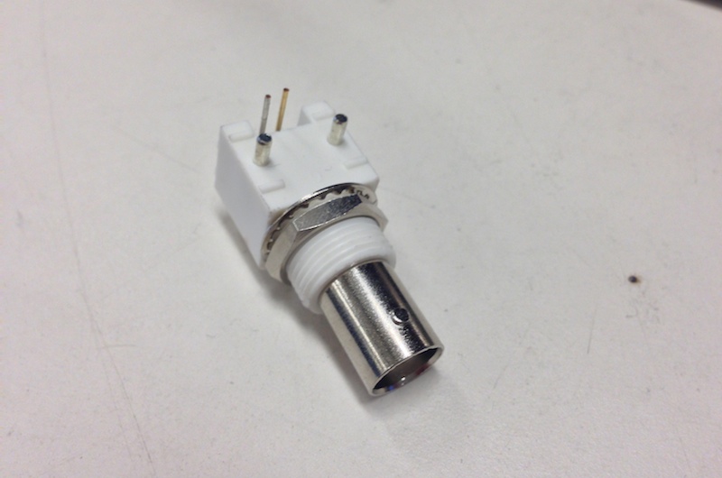
The BNC connector from SparkFun
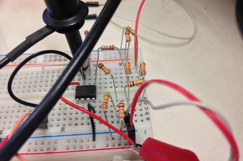
Debugging the signal conditioning circuit
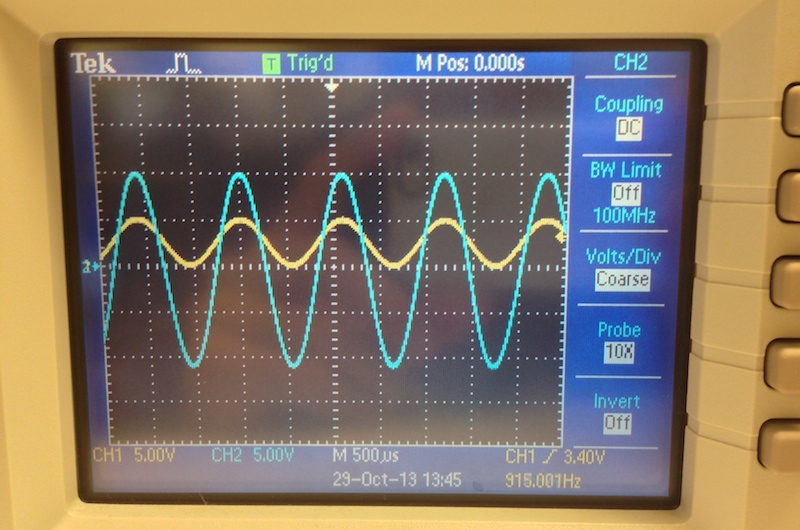
The signal conditioning circuit taking a -10V to 10V peak to peak sine wave from the signal generator and scaling it to 0V to 5V