Project 02
Making a printed circuit board in 4 parts
- Design
- Milling (printing)
- Stuffing (soldering)
- Programming (crying)
before we can make a board, let’s design one!
Design
The whole time I was looking at the different designed boards, I was thinking, wow, these continue to get more and more efficient, but what about optimizing for fun, or beauty, or transparency. PCBs are essentially maps and they tell a story of electrons, so why not let the board help tell that story. So I thought maybe I would make an application to obey the rules of a given schematic, but allow me to modify the traces to a more appealing board design.
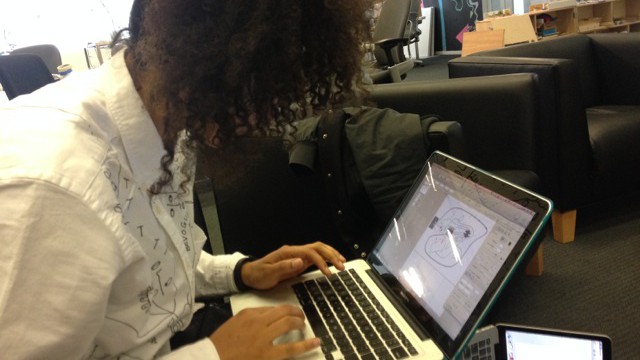
Then I pass by the 2nd Floor room in which visiting artist and Fellow, Shantell Martin has drawn a huge beautiful drawing, reminding me of all of the elements I wanted for a PCB. So I introduced myself and we sat together to discus my vision for the PCB while I listened to her explain her drawing process. It was so clear that there was an overlap and an interest in these maps of different scale, so we decided to meet up after I had prepped some tools to allow us to explore together.
Eagle. Your standard tool for designing boards. OmniGraffle. Your standard tool for… Well, it is a flow chart software that is used for all sorts of wonders, and I thought the nature of a flow chart and the object being able to maintain connections would allow for a great trace editing experience without ruining the boards functionality.
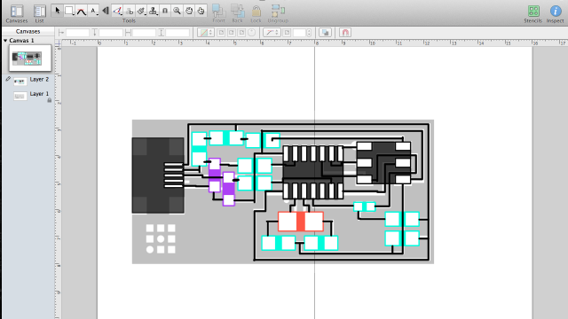
Using OmniGraffle to create all of the components on the board and connect them with traces.
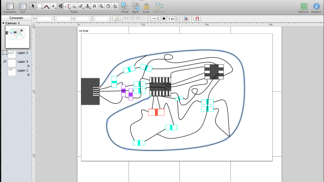
Now that the traces are all connected, we can move components around freely and maintain the schematic layout of the board.
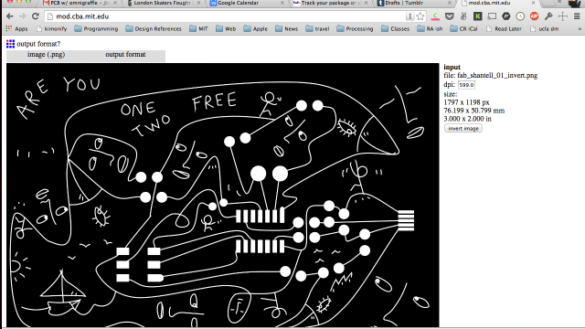
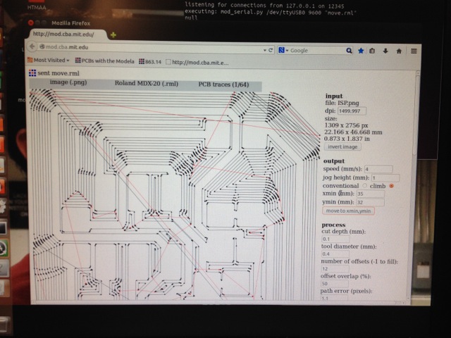
Upload the png at the correct size and inverted to carve away all of the black and leave the traces.
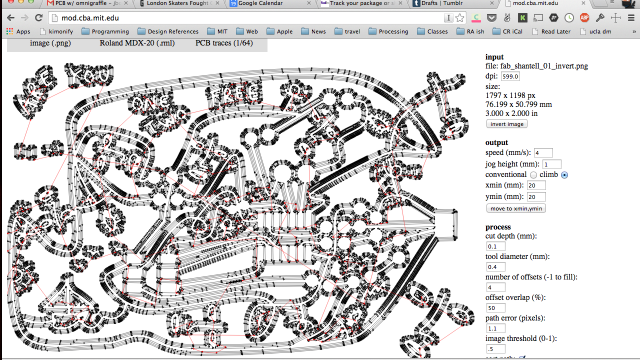
Fab Module takes the exported png (sized 2×3″ for the board) and computes the tool paths, notice the circular solder points could be problematic.
Shantell working in Omnigraffle before switching to illustrator to fill in the whitespace.
note: Shantell played with the fab module to get a sense of what the tool will do, and after seeing the milling process and final product, we both agree, we can take advantage of component placement better and get a better sense of the final composition.
Milling
Milling came with its own set of issues, but first I’ll explain the basics.
- Milling boards is quick, easy, cheap, and non-toxic
- Milling boards requires careful calibration of the tools
- Milling boards requires careful overview of the path going to be milled
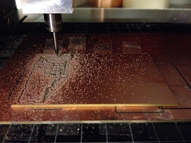
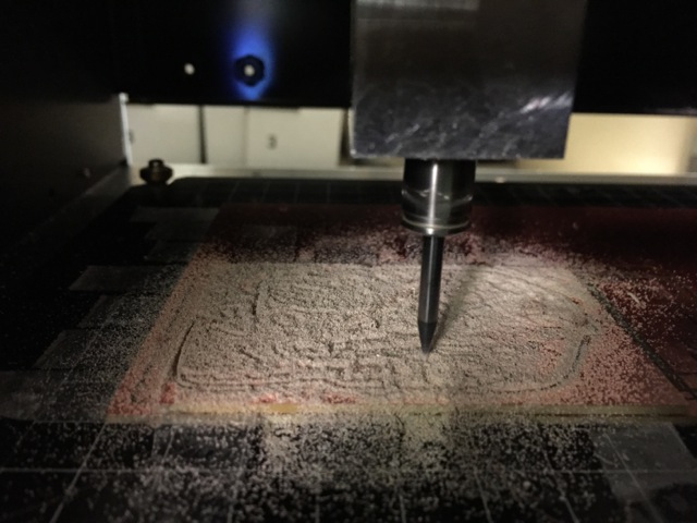
Once again, the fab modules took care of creating the pathing and sending to the CNC mill (a small desktop one).
Settings were left at the defaults, although playing with the tooling size (i.e. changing .4mm tool width to .3mm) for some boards made some shorts obsolete, but introduced other issues such as incredibly skinny traces. This makes sense given that the actual tool width is around .4mm thick.
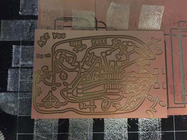
Notice the black line cutting across the traces? I didn’t, but that was unfortunately due to a bug and my interest in having the mill remove all excess copper.
Milling is looking good, so I thought
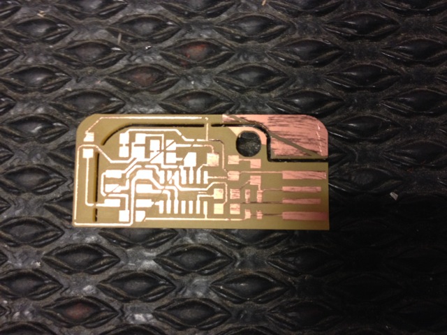
Came out pretty nice, except for those few lines cutting straight through the board. Actually, I also noticed some other shorts, so it made sense to remake this board anyway.
Milling the fabISP Shantell edition.
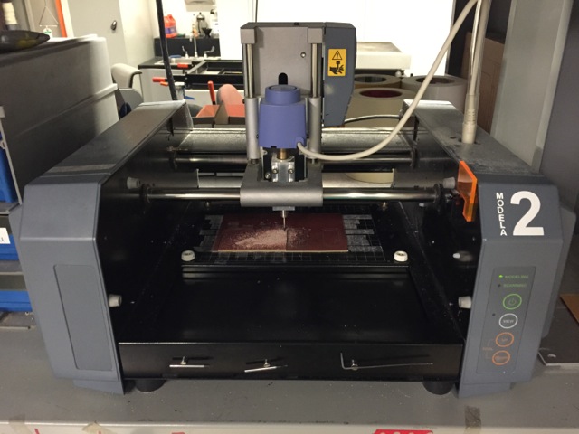
The desktop milling machine.
Figured I would try making one out of the copper tape as well, but this proved to be much more difficult. I’ll definitely return to this machine, but perhaps with a more kind layout
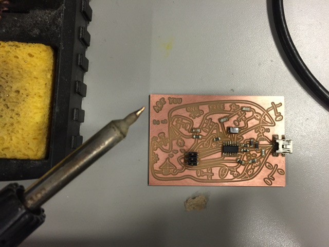
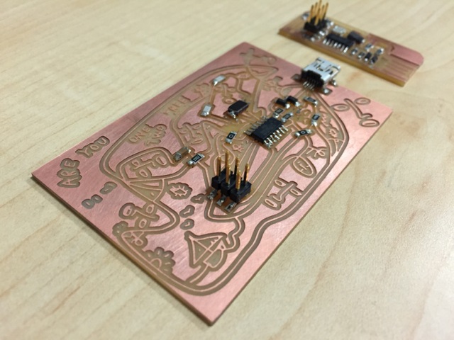
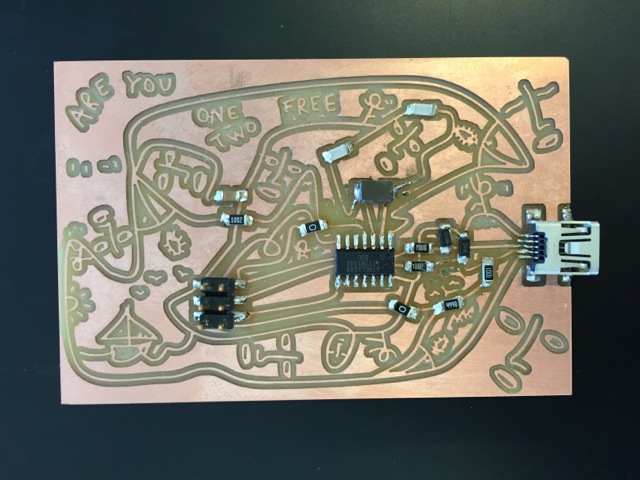
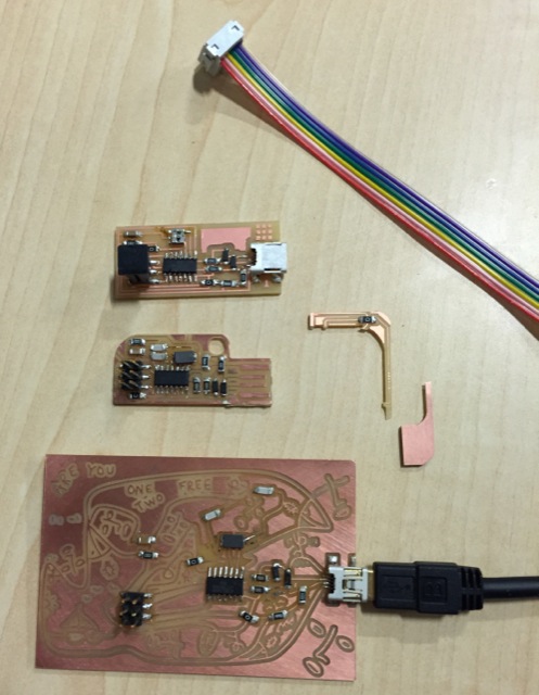
Stuffing
To make it easy in the parts room, I made a list of all of the components I would need for each of the boards.
Note: DO NOT PLACE UNLABELED CAPACITORS ON THE TABLE, it becomes confusing and then you have to throw out parts. Sadly, surface mount caps are not labeled.
SnapISP (Valentine)
————————–
1 x 2×3 Male Headers
1 x ATTiny44a
2 x Zener-diode
1 x 20 MHz Osc
Resistors
- 2 x 0 Ohm
- 2 x 100 Ohm
- 1 x 499 Ohm
- 1 x 1K Ohm
- 1 x 10K Ohm
Capacitors
- 2 x 18pF
- 1 x 0.1uF
FabISP
————————–
1 x 2×3 Male Headers
1 x ATTiny44a
1 x J2 USB
2 x Zener-diode
1 x 20 MHz Osc (Crystal or Resonator depending on design)
Resistors
- 1 x 1K Ohm
- 1 x 499 Ohm
- 2 x 100 Ohm
- 2 x 0 Ohm
- 1 x 10K Ohm
Capacitors
- 2 x 10pF (for 20MHz crystal)
- 1 x 1uF
Programming
Since there are great tutorials on programming, I will just link to them here and include a couple of notes that helped me.
- Plug in your board to the USB (If it doesn’t smoke, you are off to a good start)
- Plug in your board to the FabISP or AVRISPmk2 (Green light is good, check this chart of status lights)
- Edit the makefile to use either the FabISP or the AVRISP
I spent a lot of time thinking I had poor solder joints because I had actually plugged my AVR programmer 6pin cable on backwards. Orange blinking is a status that suggests it is backwards. Note that the FabISP needs power as well, so plug in both the programmer and the FabISP correctly to get a green light.
In Terminal, navigate to the folder containing your firmware (make files and such) and then run the following commands in this order:
- make clean
- make hex
- sudo make fuse
- sudo make program
If all is a success, you have some desoldering to do. Once the “0” resistors or jumpers are removed, you should be good to test and program boards from your FabISP. To make sure that your board is recognized by the computer you can call the following command in Terminal.
system_profiler SPUSBDataType | grep “FabISP”
If it prints/returns FabISP: then you are good to go!
(My only board to successfully pass these tests was my last board using the 20MHz resonator) I wonder if the lack of 18pF capacitors and substitute of 10pF capacitors is causing any problems with the crystal.
Final boards, programmed and ready to go… Sort of. The only one that actually works is the resonator FabISP.