Wherein Aubrey learns how to use EDA tools through almost pure trial and error.
Goals:
As someone who hasn't done much electronics design before, this week was pretty intimidating. I had to spend a lot of the begining of it gathering some resources on the absolute basics of how any of this works. Thankfully, the sites of students from previous years were a really helpful base of useful tutorials. To continue the tradition, here are some of the best that I found for getting started:
I wanted to use KiCAD, rather than Eagle, because I don't want to end up in a situation years from now where I'm not attached to a university and can't get a free student license. As someone who already knows Maya but not Blender, and all of the Adobe Cloud, but not GIMP, I'd prefer to start with the version that I know I'll always be able to use. I also just really like and believe in the ethos of the open source community. This video was really helpful in getting me started.
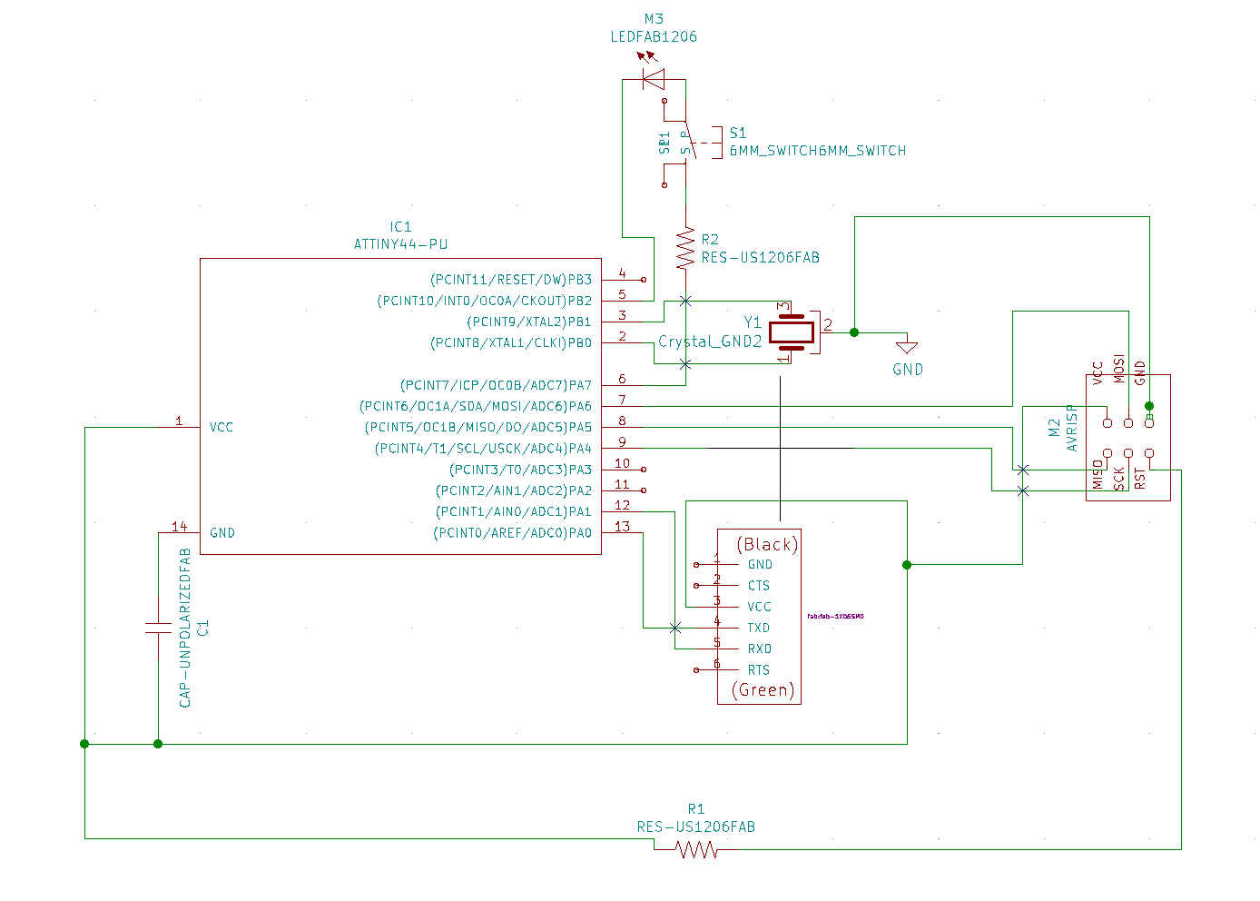
The goal was to make this board, then add a button and a switch. I started making it in KiCAD using more or less the same method I used two weeks ago for electronics fabrication: make it look like the picture.
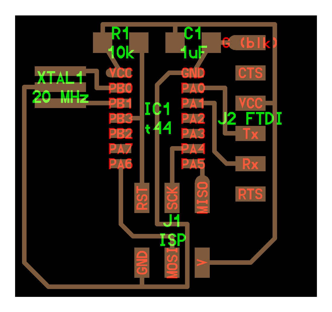
The libraries of every part which should be actively available in the fabinventory live here. To add a library, download the .lib file. If you've put it in the right place relative to all of your other files, it will turn up in the home screen. Clicking on it will open a sort of library editor. Under "File", there's a "New Library" option, which will let you link that library. Then, when you're placing parts in the schematic, you can filter for just parts that you know you have access to by searching the name of the library. This makes figuring out exactly which of the many versions of all of these parts are the actual one you should be using. I also eventually linked both the library and the footprints using the options in the "Preferences" tab. It's unclear which of these worked, but one of them did.
I did not figure out how to connect the correct library until after several hours of...
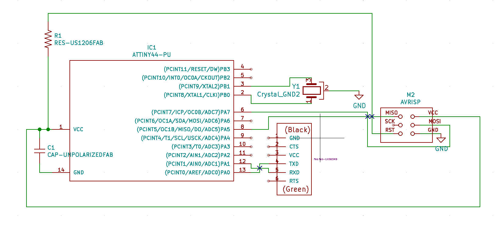
...getting comfortable with the scematic editor.
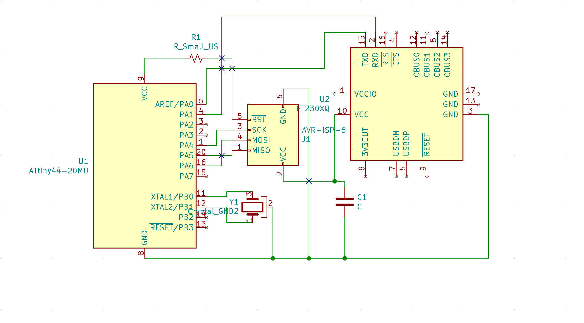
At this point, I had Zach take a look at my schematic. While you can learn a lot from pure brute force trying things and intuition, I do recommend having someone who knows what they're doing take a look at your board at this point, before you moved on. Mine had an FTDI chip, rather than an FTDI connector. These are very different things. Then, I realized that I had no idea what the footprints for any of my parts were, because I got them from the wrong library.
After connecting everything in the schematic, use this button to associate a footprint with each of your components.

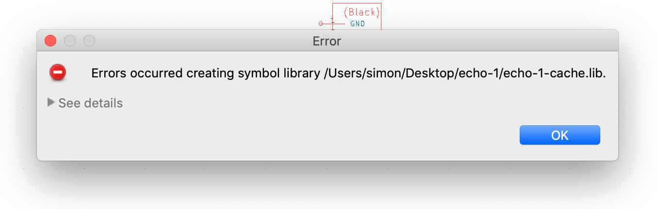
You may get any one of the following lovely Gallery of Errors:
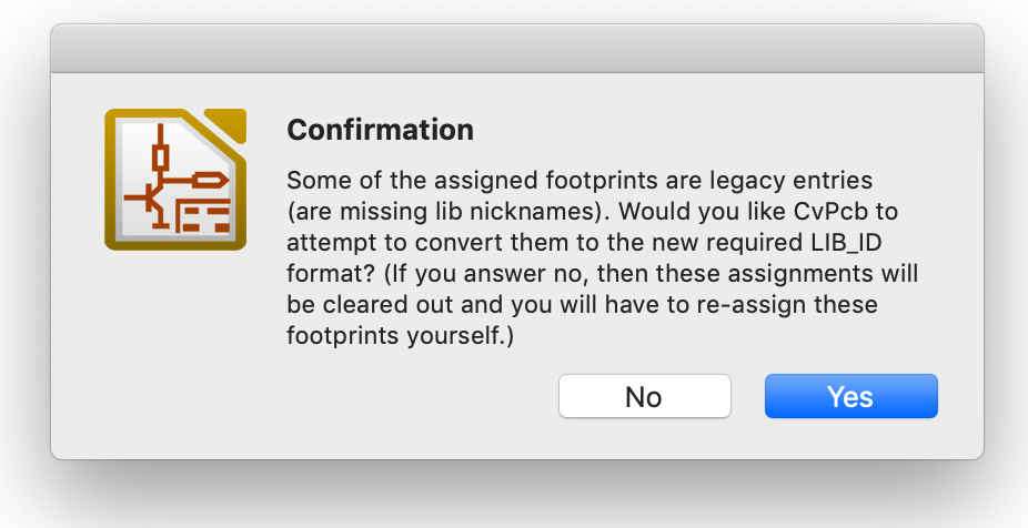
You aren't using the right parts. Or, you haven't correctly associated footprints with them. In hindsight, I recommend getting all of what you think the right parts are, then trying to connect all of the footprints, and generating the netlist, before you do any kind of actual work on the schematic or routing. It will save you from the process of routing the wrong parts, or parts which you don't actually have footprints for, over and over again.
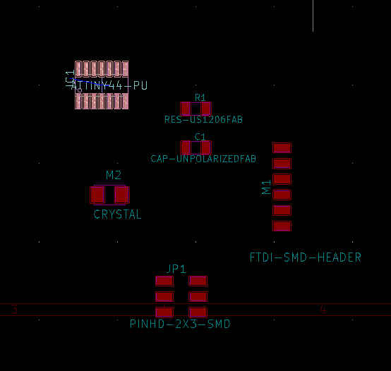
Hopefully the right set of footprints?
After you are fairly certain that you have more or less the right parts, link them together on the schematic.
Then, use this button to generate a net.

Switch to the PCB editor (which, by the way, has entirely different keyboard shortcuts), and use the same button on that side to generate your rat's nest.
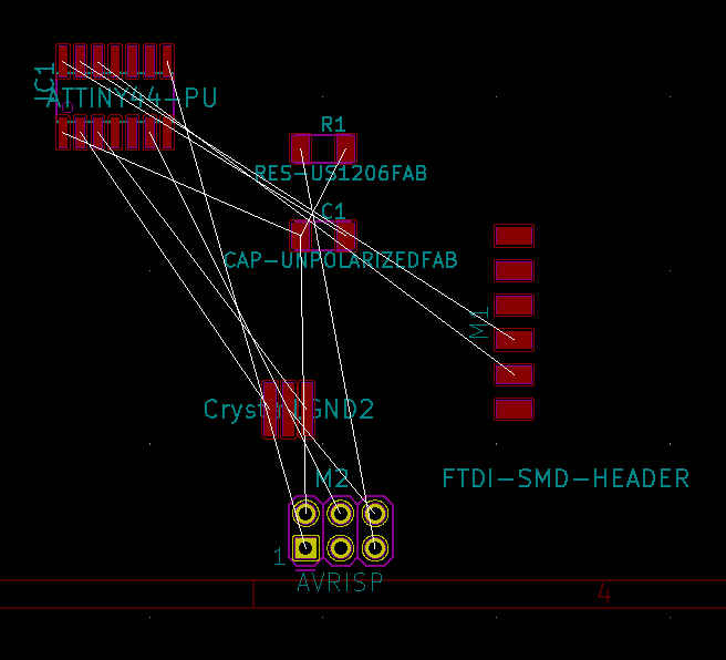
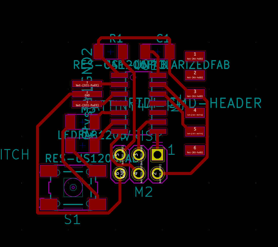
Then route it: and oddly mindless and satisfying process.
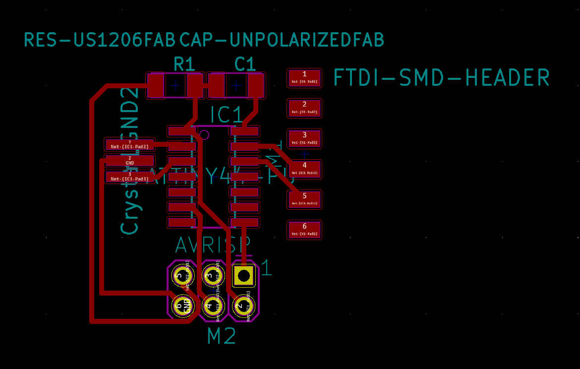
BUT. Did you remember to add the LED and button? In hindsight, it's probably better to do this before routing everything else.
Another important note about KiCAD: it doesn't autosave. Save often. Learn to save often from being told to save often. Don't lose all of the work from the night before when you accidentally close the window the following morning.
It isn't pretty, but hopefully it works.
After checking in with another friend, I learned that attaching the LED to two data lines is not at all how LEDs work. I checked the work of previous students, though and it looks like people who seeemed to know what they were doing did exactly that. It seemed worth trying it.
However, if we look at the traces, the pads for the AVRSP definitely aren't right. That was not the footprint was looking for. I thought that I could glop some solder on there, and it would be fine. Metal is metal, more or less. However, because the endmill was starting to get old, and really starting to struggle with things that pushed the edges of the design rules, milling those round ends wasn't going to work. Thankfully, what mods reads in is just a PNG, and PNGs can be edited by hand.
