Electronics Production
Making an In-circuit Programmer
Files: traces and outline to characterize milling capabilities, Brian’s PCB design
This week our assignmnet was to mill a printed circuit board (PCB) using a desktop format mill, solder on it the relevant components and program it in order to make an in-circuit programmer. The board will be used later this semester to program other microcontrollers.
PCB Milling
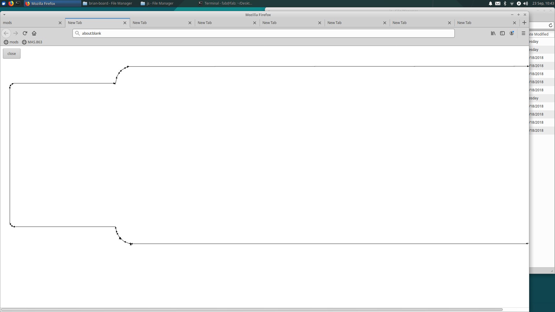
We were trained to use the Roland SRM-20 milling machine, controlled with mods. The mods interface takes black and white PNG images as input, calculates toolpaths, and sends the resulting G-code to the milling machine.
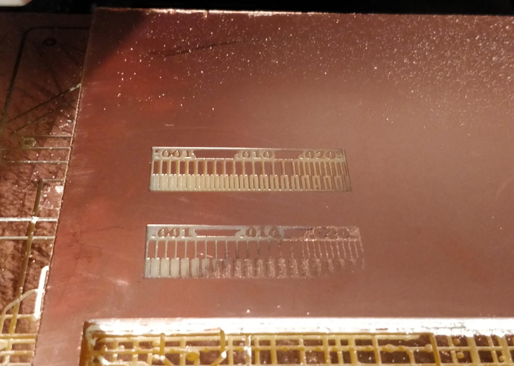
During the group assignment (team: Zach, Jiri, Aubrey, Afonso, D., and me) we milled a test file with different trace widths to characterize the the design rules for our PCB production process.

We opened the test file (internal traces) in mods and mounted the 1/64" end mill to mill our copper sheet. After setting the origin and zeroing the tool Z-axis manually, we set both the cut depth and the maximum depth at 0.004", meaning that the end mill would do a single cut at 0.004" (singl pass). We also set the offset at 2, meaning that the end mill would do a double outline. Choosing only one cut was a bit ambitious, but would save us time if the machine could acheive the expected result. We then sent the file in the machine and waited to see the result.
The outcome was not good. Part of the design was not cut at all with the single cut setting. So we reset the origin and we zeroed the end mill again and set the maximum depth at 0.008" this time in order to have two vertical passes of the end mill. All the other settings remained the same with the previous time. As expected this outcome was significantly better from the previous one. As expected, with a 1/64" end mill traces must be at least 1/64" apart, while traces thinner than a few thousandths of an inch lack structural integrity and are easily knocked off.
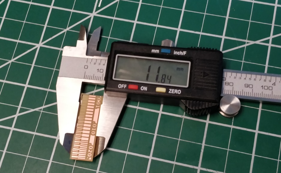
Then we mounted the 1/32" end mill to the machine and we imported the test file with the outline of the design at mods (the first time I accidentally imported the wrong file and we had to stop the milling process, import the correct file and do it again!). After taking the milled design out of the copper sheet, we decided to measure it and compare it with the width value reported in mods. Mods reported the width of the design at 12.80 mm. We expected the width of the milled part to be 12.80 - (2 * line width). Zach used used Gimp to measure the line weight at 50px. The png file imported in mods was at 2500 DPI, so the line width was 0.51 mm. So, the width of the milled part should have been 11.78 mm. We measured the width to be 11.84 mm, which is very close to what expected.
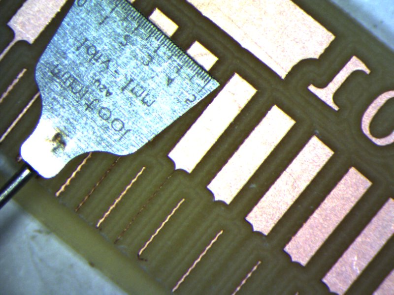
Then we used the Lynx Evo Projection Microscope to inspect the milled part in detail. We observed that fine trace lines (0.001" - 0.005") were wavy and not straight as they seamed.
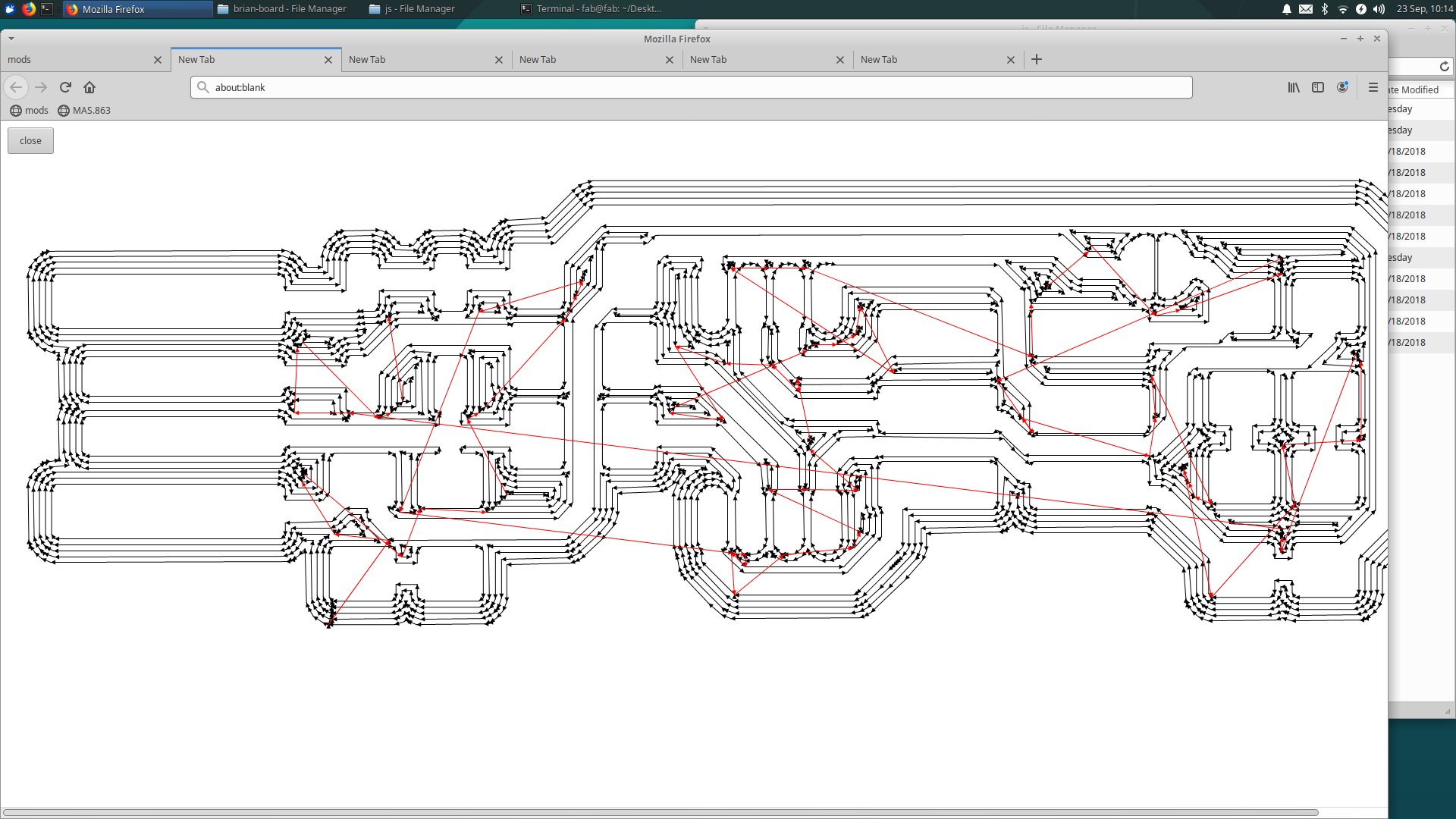
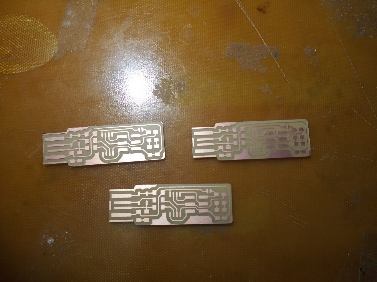
After the group assignment, I milled my PCB following Brian’s PCB design.


At the beginning I was a bit afraid not to break the end mill, so I zeroed it a bit higher than I should, and it didn't cut the copper at all! Then, I decided to overcome my fear and I zeroed the end mill exactly at the point where it touched the copper sheet and everything went well.
I milled 3 PCBS to save time in case my soldering eforts failed.
PCB Assembling
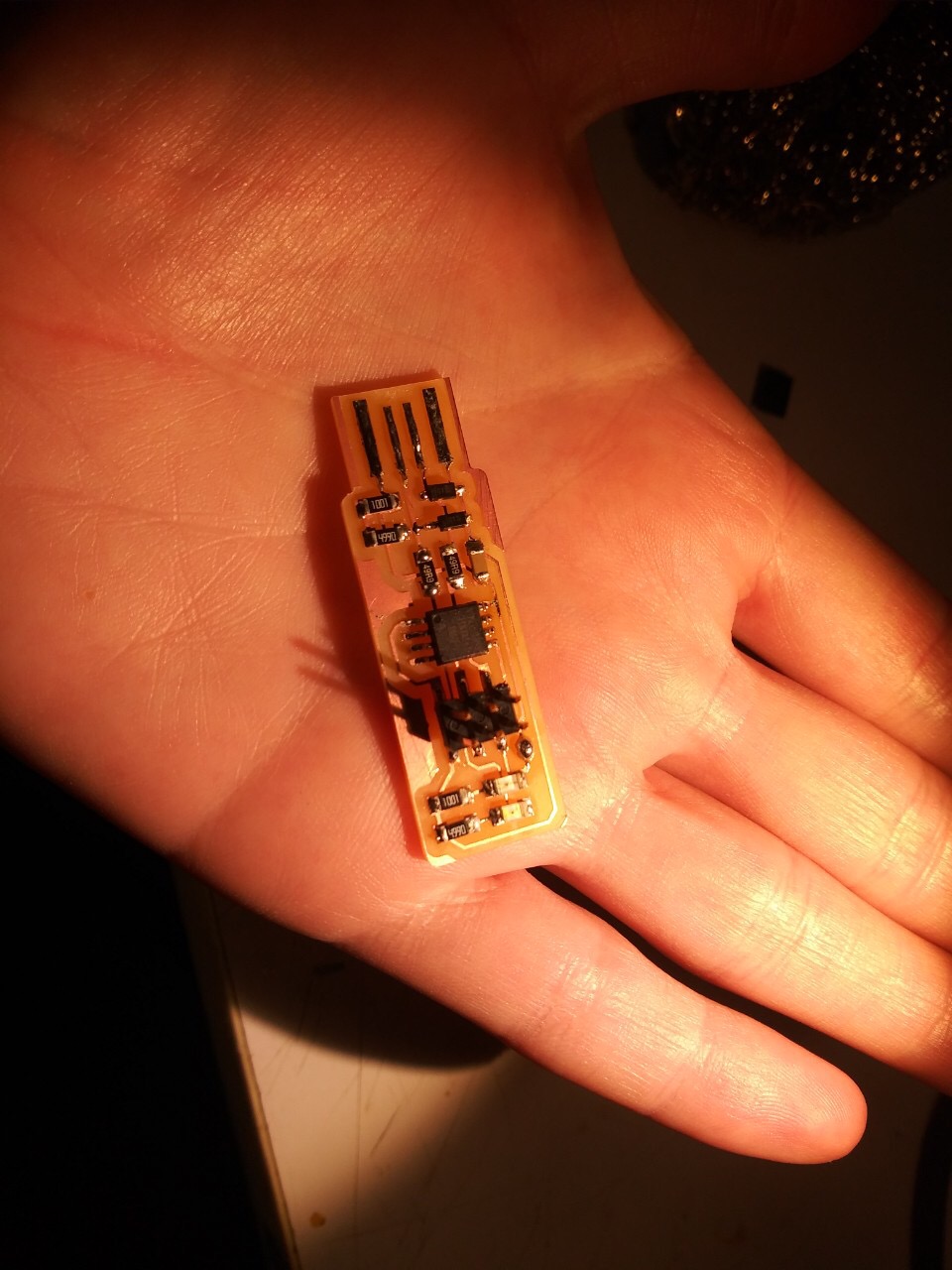
First I found the necessary components to be mounted on my board, following Brian’s notes:
- 1x ATtiny45
- 2x 1kΩ resistors
- 2x 499Ω resistors
- 2x 49Ω resistors
- 2x 3.3v zener diodes
- 1x red LED
- 1x green LED
- 1x 100nF capacitor
- 1x 2x3 pin header
I had never tried soldering before, and (guess what!) I was a bit afraid to do it. Thank god Zach sat with me and showed me how it is done (thanks so much Zach). So, I felt more comfortable and I did it! It was fun actually and way more easy than I thought. I am so happy, my board came out smooth and shinny as it should!
PCB Programming
I followed Brian’s instructions for Windows and programmed the ATtiny45 using the Atmel-ICE programmer, using the Atmel Studio 7.
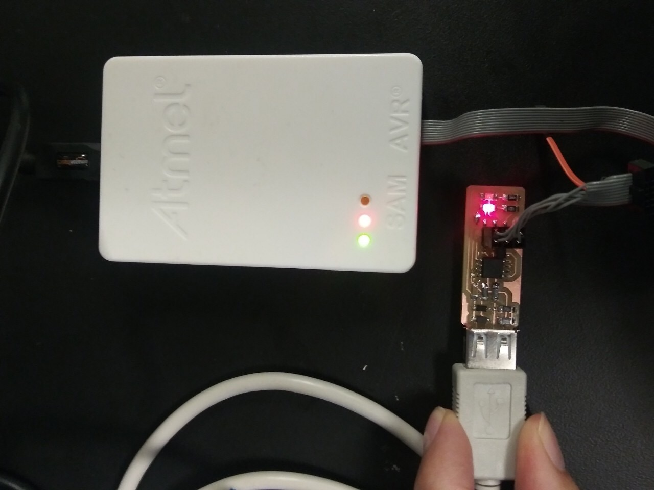
Then, I tested the USB functionality, as the programmer was listed in the Device Manager of my laptop as USBtiny device. Finally, I disconnected the VCC from the Vprog pin on the ISP header by removing the bridge on the solder jumper. The excess solder stuck to the soldering iron tip, thus breaking the connection.
