Overview
Workload: ● ● ● ● ○
Previous Knowledge: ○ ○ ○ ○ ○
Current Knowledge: ● ● ● ○ ○
Concepts
Electronics, Components, PCB Design, Milling, Soldering
Software
EAGLE (Fusion 360), Mods, SVG-PCB
Assignments
1. Use the test equipment in your lab to observe the operation of a microcontroller circuit board [Group]
2. Redraw and echo hello-world board
2.a. Add (at least a button and LED (with current limiting resistor)
2.b. Check the design rules, make it, and test that it can communicate
Extra credit: Simulate its operation
Documentation
Electronics design was the most challenging week so far. Although the assignments were clear and not too long, my lack of conceptual knowledge about made it very difficult to understand the role of each component in the board and how I should organize them in order to function properly.
After spending a lot of time on tutorials and several videos about the basics of electronics, my strategy was to replicate existing designs and later try to customize them.
Theory
Before trying to design the board, I spent time trying to catch up and build a better conceptual foundation about electronics in general. The recitation as well as the tutorials created by the TAs were extremely helpful to learn more about design software such as KiCad, Eagle and SVG-PCB. Also, I watched several videos that explained simple concepts such as voltage, current and resistance.
Electricity: flow of free electrons between atoms.
Voltage (V): the difference in charge between two points. It is like the "pressure" that pushes free electrons around a circuit, causing current. Without it, electrons move randomly in any direction.
Current (A): the rate at which charge is flowing.
Resistance (Ω): material's tendency to resist the flow of charge (current)
Ohm's Law: V = I x R
Components
There are several different components that can be placed in a circuit. The following are those that were required in the PCB designed this week:
• Microcontroller: compact integrated circuit designed to govern a specific operation in an embedded system.
• Voltage Regulator takes an input voltage and give a steady output. In this case, it takes an input (could be between 4 and 30V) and give a 3.3V output that the microcontroller will use.
• Capacitor: stabilizes the output of the voltage regulator. Think of them as a battery - once they charge up to a specific voltage they try to maintain that voltage.
• Resistor: limits or regulates the flow of electrical current in an electronic circuit.
* Zero-ohm resistors are very useful to jump a wire over another.
• Programming Pins: just a physical connection that will be used to send programs to our boards.
• USB Connector: connection to transfer power to the board as well as load programs.
• LED (light emitting diode): to emit light and potentially useful for debugging purposes.
* LEDs are directional (cathode - green mark - should go towards ground). Rule of thumb: 1.3V and capable of handling ~20mA.
• Button: connect one side to pin of microcontroller and another one to ground.
Practice
Since I had previously worked with Fusion 360, I chose to design my board using EAGLE.
Designing
Initially, I followed the entire EAGLE tutorial to become more comfortable with the software.
Tutorial: EAGLE in 10 Commands
There are two main views and a few commands that are very helpful while designing the board:
Schematic View: simple two-dimensional circuit design showing the functionality and connectivity between different components.
• Add: to add components to the sheet.
• Delete: to delete components and remove nets.
• Net: to draw a kind of non-physical wire - or we can think of it as a vertex in a graph to which other things (component pads, for example) are connected.
• Move: to move components, wires, etc. When moving, we can right-click to rotate by 90o.
• Name: to give nets unique names. Drawing two net lines but naming them the same thing will “virtually” connect them, meaning you can make schematics less messy.
• Grid: The grid is how we keep ourselves organized in Eagle, or line things up. You can set grid units.
Board View: the circuit board, the data for the physical bit that the electronic circuit is on.
• DRC (design rule check): lets you configure Eagle such that it won’t let you draw signals that are i.e. too close to one another (such that they would be impossible to manufacture). It also helps check for errors: make sure you call DRC before you send a board to fabrication.
• Route: lets us connect disparate elements of the same net to one another.
• Ripup: Contrary to route - ripup will remove tracks / traces, or delete vias. Ripup has some settings: we can remove partial elements of a trace, or vias, or the entire signal, or only the piece of a signal on the current copper layer.
• Polygon: The polygon command lets us draw copper “pours” - areas we want to cover with monolithic sweeps of connected copper.
• Rastnest: to re-draw all polygon pours, and in older versions of Eagle, will redraw the airwires as well.
• Show: to highlight signals / nets in our board design. For example show +3v3 will highlight everything connected to the +3v3 net, you get the idea.
• Display: To show/hide specific layers during routing.
1. I started a New Electronics Design on Fusion 360 and launched the EAGLE environment.
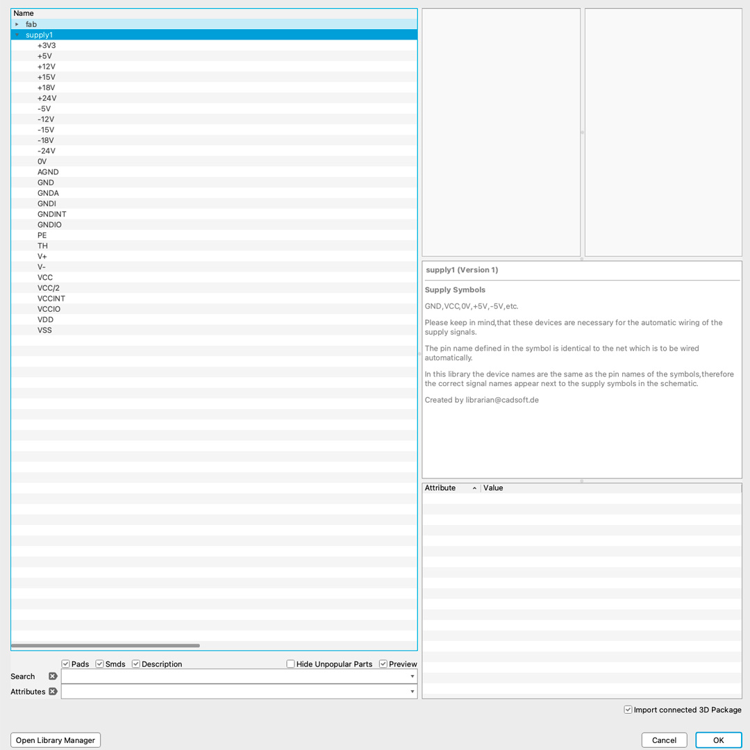
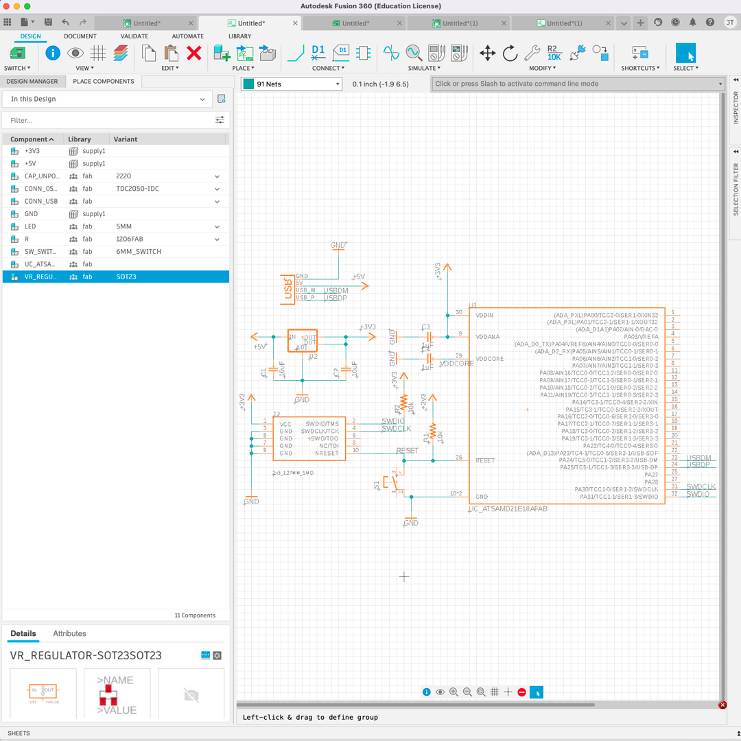
2. In the schematic view, I included two component libraries: fab and supply1. The first includes all components available for us in the lab and the second includes useful components and signs.S
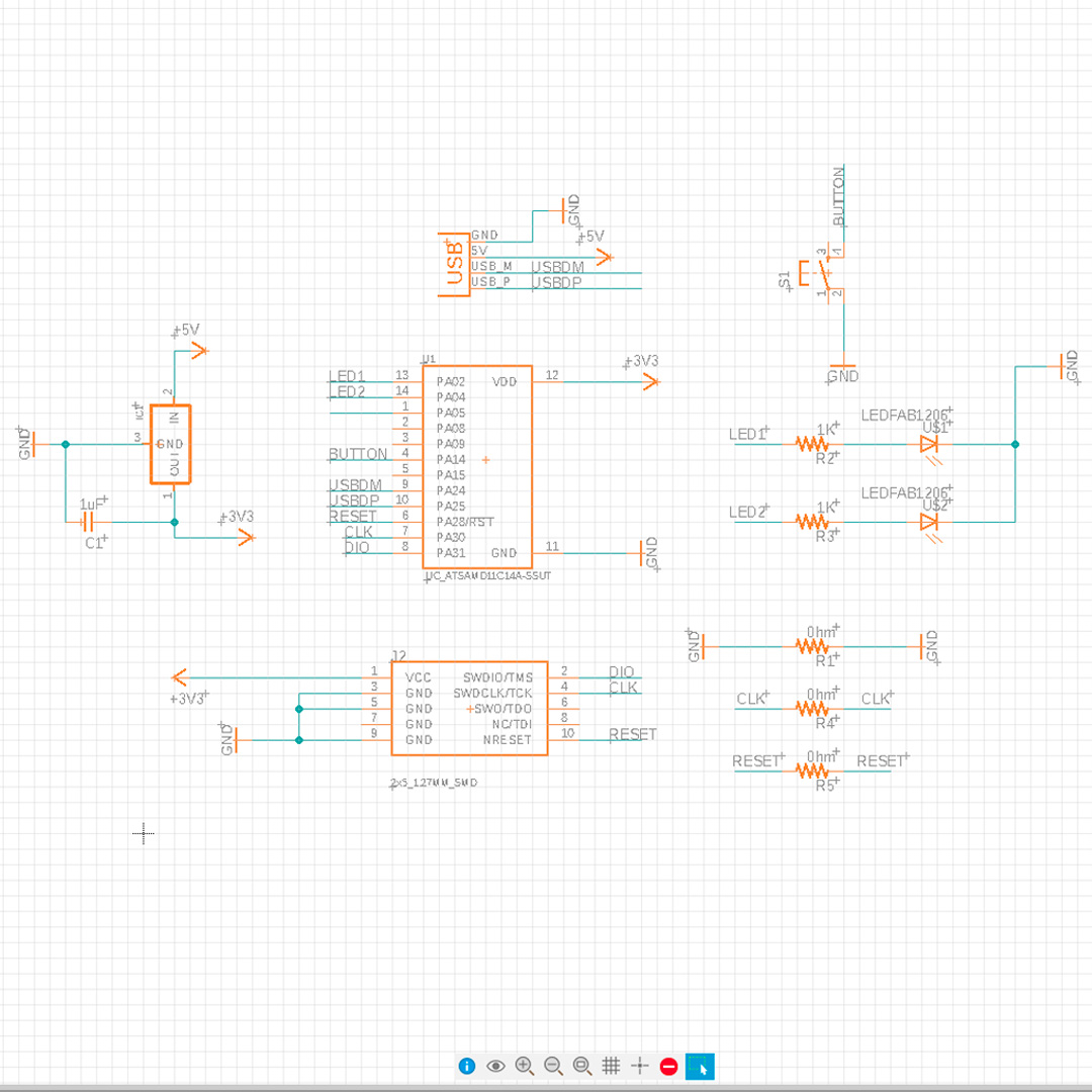
3. Although there were several boards that could be used as a reference for the design, I decided to follow and create exactly the same design showed in the tutorial - with the microcontroller ATSAMD21E.
However, I was struggling to understand how I should add the additional components and I thought it would make more sense to create a board that was similar to that printed in week 03.
4. I searched for some references from previous classes and found this one that was well documented. Using the same components, I was able to recreate a similar design - a 10 pin ATSAMD11C board.
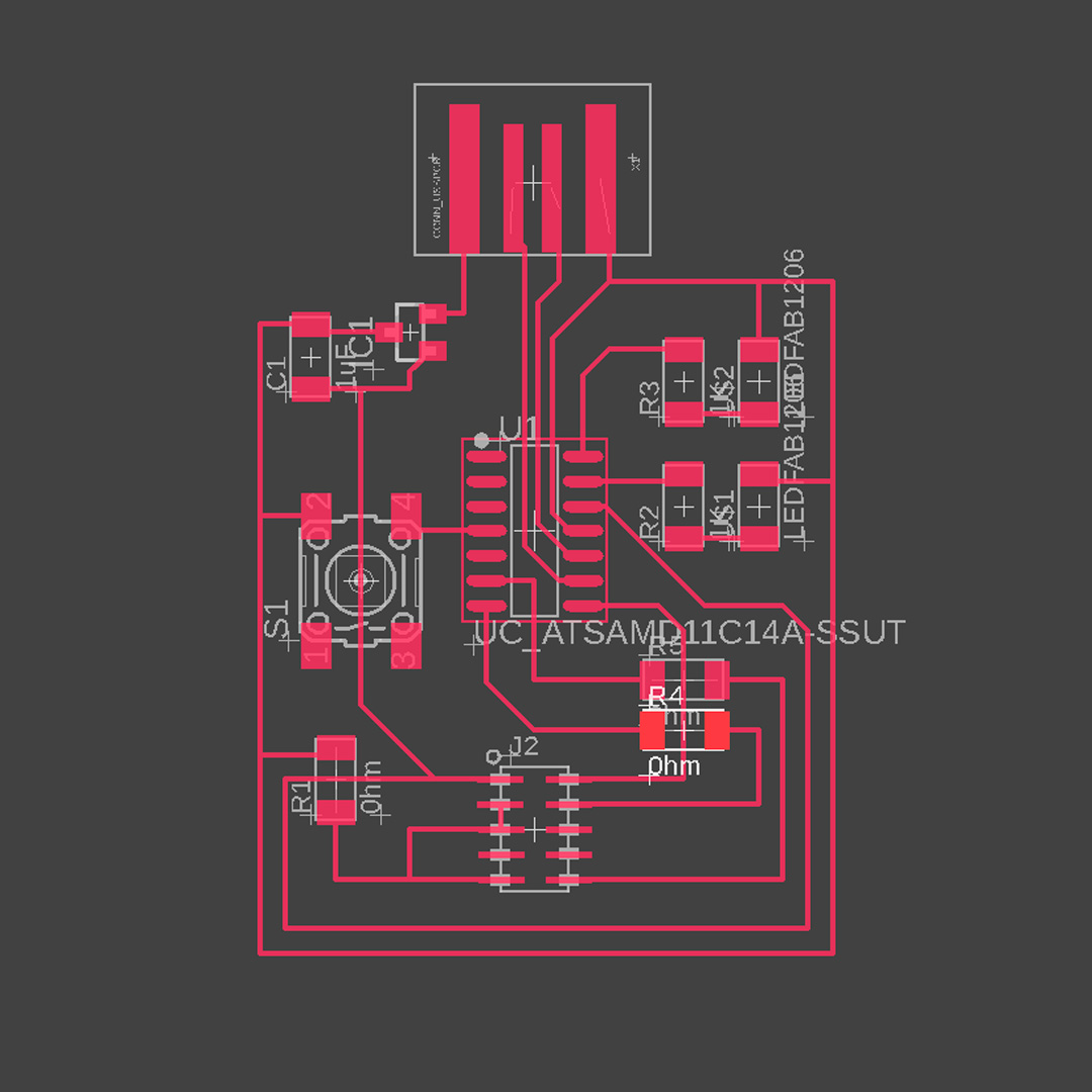
The most important steps I followed during the process were:
• Add components in the schematic view
• Draw nets to connect pins
• Add names and "automatically connect" points with same name
• Add values to respective components
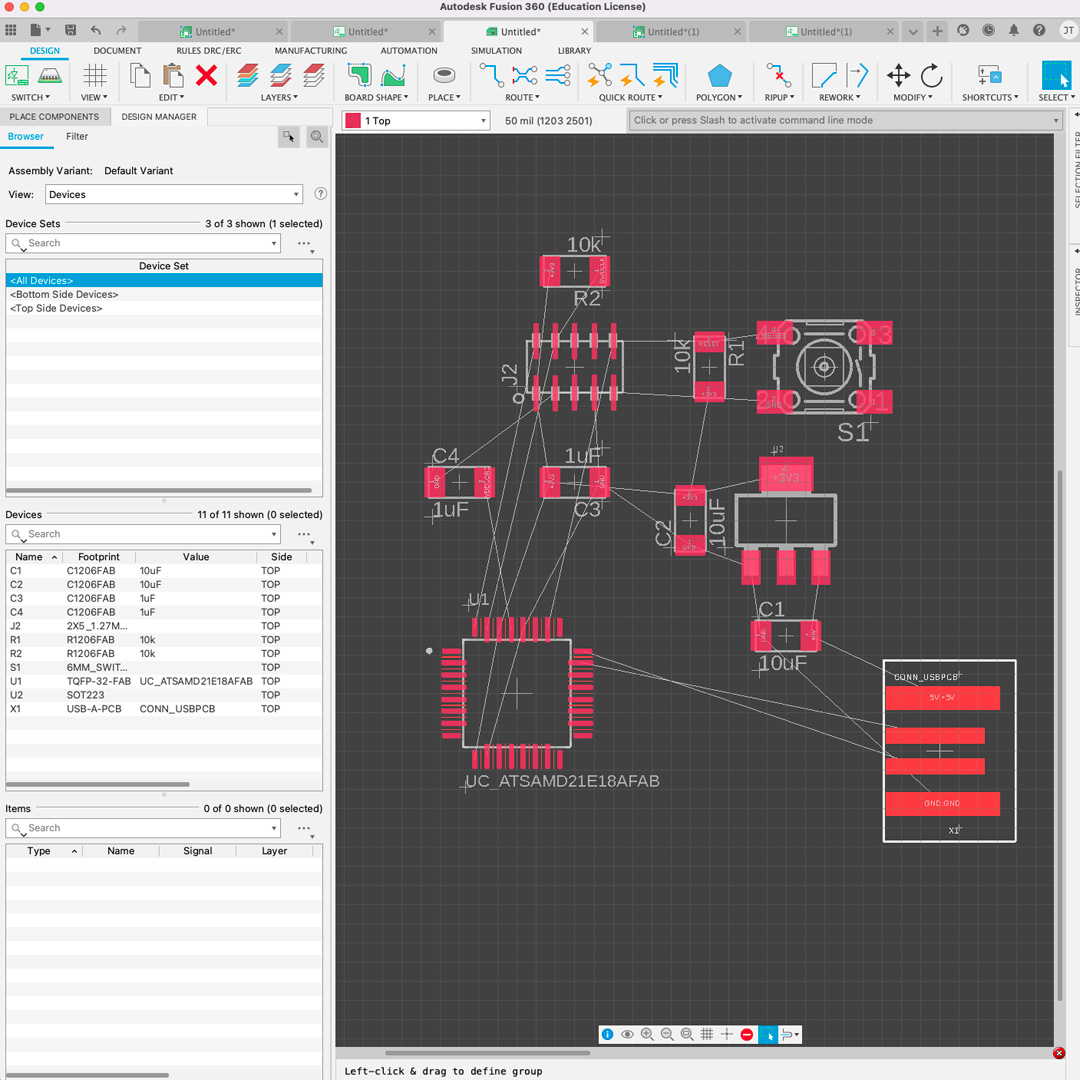
• Position components in the board view
• Add traces and start resolving paths
• Run DRC to check potential issues
• Draw the outline in the respective layer
• Generate .png files
Printing
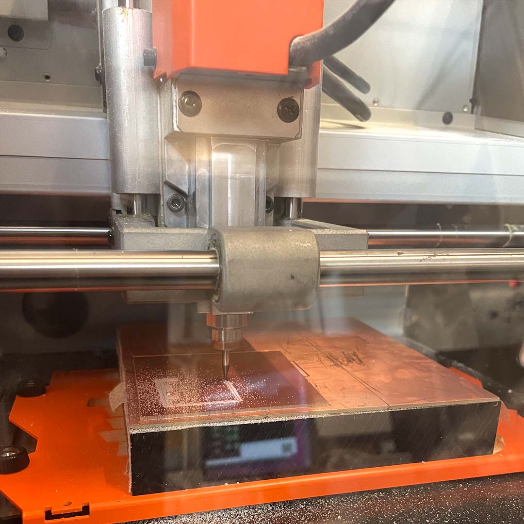
5. For printing, I followed the same processes learned in Week 03 and obtained the following board.
Soldering
6. Soldering was also similar to Week 03, but given the thin traces, it was very hard to solder all the components. After some time, I was able to put all of them, but some connections still look weak.
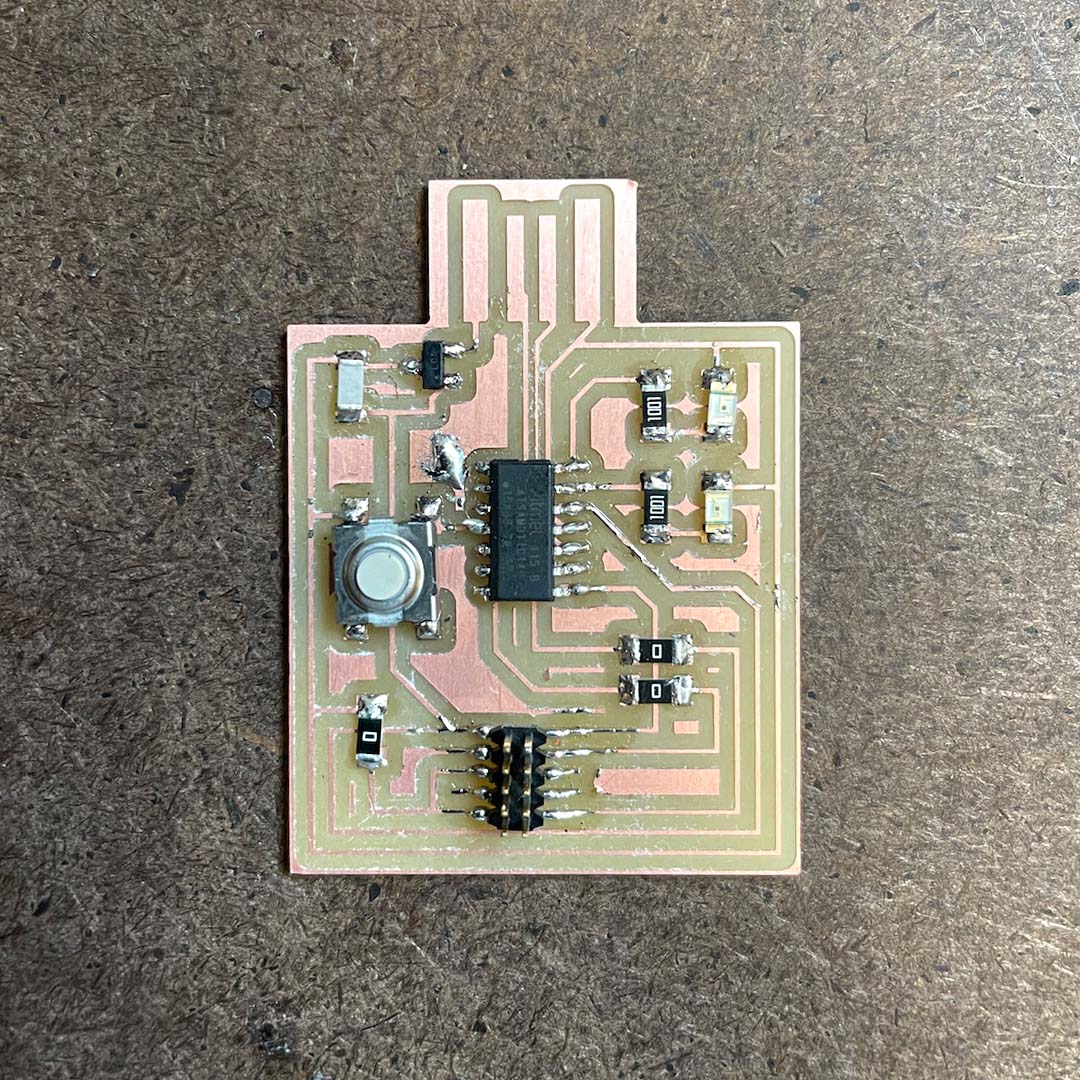
Testing
7. I will test my board later this week. But, honestly, I'm not confident that it is going to work properly, especially because of the thin traces and some issues with soldering.
Overall, electronics design has been a big challenge. I still need to become more comfortable with the concepts behind the design and the rules to create a functioning board. I plan to spend the next few weeks practicing and learning more about it.
Files